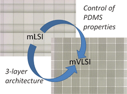
Microfluidic chips with a high density of control elements are required to improve device performance parameters, such as throughput, sensitivity and dynamic range. In order to realize robust and accessible high-density microfluidic chips, we have fabricated a monolithic PDMS valve architecture with three layers, replacing the commonly used two-layer design. The design is realized through multi-layer soft lithography techniques, making it low cost and easy to fabricate. By carefully determining the process conditions of PDMS, we have demonstrated that 8 × 8 and 6 × 6 μm2 valve sizes can be operated at around 180 and 280 kPa differential pressure, respectively. We have shown that these valves can be fabricated at densities approaching 1 million valves per cm2, substantially exceeding the current state of the art of microfluidic large-scale integration (mLSI) (thousands of valves per cm2). Because the density increase is greater than two orders of magnitude, we describe this technology as microfluidic very large scale integration (mVLSI), analogous to its electronic counterpart. We have captured and tracked fluorescent beads, and changed the electrical resistance of a fluidic channel by using these miniaturized valves in two different experiments, demonstrating that the valves are leakproof. We have also demonstrated that these valves can be addressed through multiplexing.

You have access to this article
 Please wait while we load your content...
Something went wrong. Try again?


 Please wait while we load your content...