Parylene to silicon nitride bonding for post-integration of high pressure microfluidics to CMOS devices†
Abstract
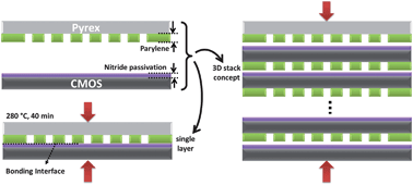
High pressure-rated channels allow microfluidic assays to be performed on a smaller footprint while keeping the throughput, thanks to the higher enabled flow rates, opening up perspectives for cost-effective integration of CMOS chips to microfluidic circuits. Accordingly, this study introduces an easy, low-cost and efficient method for realizing high pressure microfluidics-to-CMOS integration. First, we report a new low temperature (280 °C) Parylene-C wafer bonding technique, where O2 plasma-treated Parylene-C bonds directly to Si3N4 with an average bonding strength of 23 MPa. The technique works for silicon wafers with a
 Please wait while we load your content...

