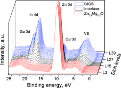
The electronic band structure at the Zn1−xMgxO/Cu(In0.7Ga0.3)Se2 interface was investigated for its potential application in Cd-free Cu(In,Ga)Se2 thin film solar cells. Zn1−xMgxO thin films with various Mg contents were grown by atomic layer deposition on Cu(In0.7Ga0.3)Se2 absorbers, which were deposited by the co-evaporation of Cu, In, Ga, and Se elemental sources. The electron emissions from the valence band and core levels were measured by a depth profile technique using X-ray and ultraviolet photoelectron spectroscopy. The valence band maximum positions are around 3.17 eV for both Zn0.9Mg0.1O and Zn0.8Mg0.2O films, while the valence band maximum value for CIGS is 0.48 eV. As a result, the valence band offset value between the bulk Zn1−xMgxO (x = 0.1 and x = 0.2) region and the bulk CIGS region was 2.69 eV. The valence band offset value at the Zn1−xMgxO/CIGS interface was found to be 2.55 eV after considering a small band bending in the interface region. The bandgap energy of Zn1−xMgxO films increased from 3.25 to 3.76 eV as the Mg content increased from 0% to 25%. The combination of the valence band offset values and the bandgap energy of Zn1−xMgxO films results in the flat (0 eV) and cliff (−0.23 eV) conduction band alignments at the Zn0.8Mg0.2O/Cu(In0.7Ga0.3)Se2 and Zn0.9Mg0.1O/Cu(In0.7Ga0.3)Se2 interfaces, respectively. The experimental results suggest that the bandgap energy of Zn1−xMgxO films is the main factor that determines the conduction band offset at the Zn1−xMgxO/Cu(In0.7Ga0.3)Se2 interface. Based on these results, we conclude that a Zn1−xMgxO film with a relatively high bandgap energy is necessary to create a suitable conduction band offset at the Zn1−xMgxO/CIGS interface to obtain a robust heterojunction. Also, ALD Zn1−xMgxO films can be considered as a promising alternative buffer material to replace the toxic CdS for environmental safety.
You have access to this article
 Please wait while we load your content...
Something went wrong. Try again?
Please wait while we load your content...
Something went wrong. Try again?