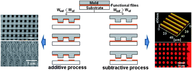
Adhesive lithography for fabricating organic electronic and optoelectronics devices
Abstract
Improvements in organic electronic materials have led to novel device applications, ranging from large-area flexible displays to lightweight plastic electronics. Progress on these applications would benefit from development of low-cost fabrication techniques for organic semiconductors. In this review, several fabrication processes based on adhesion force (i.e. van der Waals forces,

- This article is part of the themed collection: Lithography

 Please wait while we load your content...