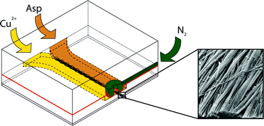
Progress in microelectronics, sensors and optics is strongly dependent on the miniaturization of components, and the integration of nanoscale structures into applicable systems. In this regard, conventional top-down technologies such as lithography have limits concerning the dimensions and the choice of material. Therefore, several bottom-up approaches have been investigated to satisfy the need for structures with large aspect ratios in the nanometre regime. For further implementation, however, it is crucial to find methods to define position, orientation and length of the nanowires. In this study, we present a microchip to trap in situ formed bundles of nanowires in microsized cages and clamps, thereby enabling immobilisation, positioning and cutting-out of desired lengths. The microchip consists of two layers, one of which enables the formation of metal–organic nanowires at the interface of two co-flowing laminar streams. The other layer, separated by a thin and deflectable PDMS membrane, serves as the pneumatic control layer to impress microsized features (“donuts”) onto the nanowires. In this way, a piece of the nanowire bundle with a prescribed length is immobilised inside the donut. Furthermore, partly open ring-shaped structures enabled trapping of hybrid wires and subsequent functionalisation with fluorescent beads. We believe that the method is a versatile approach to form and modify nanoscale structures via microscale tools, thereby enabling the construction of fully functional nanowire-based systems.


 Please wait while we load your content...