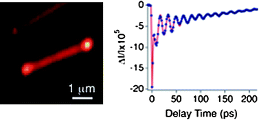
The past decade has seen tremendous progress in the development of absorption based techniques for studying single semiconductor and metal nanoparticles. These techniques complement the more common emission and Rayleigh scattering measurements. The advantages of absorption-based detection are that a wider range of materials can be examined compared to emission, and smaller particles can be studied than is possible with Rayleigh scattering. These advantages are somewhat offset by increased difficulty. Importantly, by employing absorption based detection with a pump and probe beam, transient absorption experiments can be performed on single nanostructures. This allows dynamics measurements on ultrafast (sub-ps) timescales, and is the focus of this mini-review. These experiments provide information about how processes such as electron–phonon coupling, energy dissipation, and charge carrier trapping vary between nanostructures, as well as how they depend on environment.
You have access to this article
 Please wait while we load your content...
Something went wrong. Try again?


 Please wait while we load your content...