Fabrication of nanocluster silicon surface with electric discharge and the application in desorption/ionization on silicon-mass spectrometry
Abstract
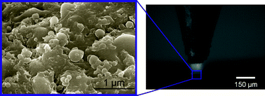
This study presents a new, simple, and low-cost technique to fabricate a nanocluster
This study presents a new, simple, and low-cost technique to fabricate a nanocluster
N. M. Suni, M. Haapala, E. Färm, E. Härkönen, M. Ritala, L. Sainiemi, S. Franssila, T. Kotiaho and R. Kostiainen, Lab Chip, 2010, 10, 1689 DOI: 10.1039/B927181C
To request permission to reproduce material from this article, please go to the Copyright Clearance Center request page.
If you are an author contributing to an RSC publication, you do not need to request permission provided correct acknowledgement is given.
If you are the author of this article, you do not need to request permission to reproduce figures and diagrams provided correct acknowledgement is given. If you want to reproduce the whole article in a third-party publication (excluding your thesis/dissertation for which permission is not required) please go to the Copyright Clearance Center request page.
Read more about how to correctly acknowledge RSC content.
 Please wait while we load your content...

