A simple method for fabricating multi-layer PDMS structures for 3D microfluidic chips
Abstract
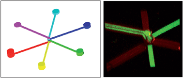
We report a simple methodology to fabricate PDMS multi-layer microfluidic chips. A PDMS slab was surface-treated by

* Corresponding authors
a
Nano Science and Technology Program and KAUST-HKUST Micro/Nanofluidic Joint Laboratory, The Hong Kong University of Science and Technology, Clear Water Bay, Kowloon, Hong Kong
E-mail:
phwen@ust.hk
Fax: +852 2358 1652
Tel: +852 2358 7979
b Department of Physics, The Hong Kong University of Science and Technology, Clear Water Bay, Kowloon, Hong Kong
We report a simple methodology to fabricate PDMS multi-layer microfluidic chips. A PDMS slab was surface-treated by

 Please wait while we load your content...
Something went wrong. Try again?
M. Zhang, J. Wu, L. Wang, K. Xiao and W. Wen, Lab Chip, 2010, 10, 1199 DOI: 10.1039/B923101C
To request permission to reproduce material from this article, please go to the Copyright Clearance Center request page.
If you are an author contributing to an RSC publication, you do not need to request permission provided correct acknowledgement is given.
If you are the author of this article, you do not need to request permission to reproduce figures and diagrams provided correct acknowledgement is given. If you want to reproduce the whole article in a third-party publication (excluding your thesis/dissertation for which permission is not required) please go to the Copyright Clearance Center request page.
Read more about how to correctly acknowledge RSC content.
 Fetching data from CrossRef.
This may take some time to load.
Loading related content
