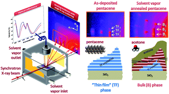
Solvent vapor annealing of an insoluble molecular semiconductor†
Abstract

- This article is part of the themed collection: Interface engineering of organic electronics
* Corresponding authors
a
Materials Science and Engineering, Division of Physical Sciences and Engineering, King Abdullah University of Science and Technology, Thuwal, Kingdom of Saudi Arabia
E-mail:
aram.amassian@kaust.edu.sa
Tel: +966(0)544700079
b
Materials Science and Engineering, Cornell University, Ithaca, NY, USA
E-mail:
ggm1@cornell.edu
c
Cornell High Energy Synchrotron Source, Cornell University, Ithaca, NY, USA
Tel: +1 607 255 0917

 Please wait while we load your content...
Something went wrong. Try again?
A. Amassian, V. A. Pozdin, R. Li, Detlef-M. Smilgies and G. G. Malliaras, J. Mater. Chem., 2010, 20, 2623 DOI: 10.1039/B923375J
To request permission to reproduce material from this article, please go to the Copyright Clearance Center request page.
If you are an author contributing to an RSC publication, you do not need to request permission provided correct acknowledgement is given.
If you are the author of this article, you do not need to request permission to reproduce figures and diagrams provided correct acknowledgement is given. If you want to reproduce the whole article in a third-party publication (excluding your thesis/dissertation for which permission is not required) please go to the Copyright Clearance Center request page.
Read more about how to correctly acknowledge RSC content.
 Fetching data from CrossRef.
This may take some time to load.
Loading related content
