DOI:
10.1039/D6TC00046K
(Paper)
J. Mater. Chem. C, 2026, Advance Article
A composition-dependent structural and gradually tunable bandgap of GeS1−xSex alloys synthesized via chemical vapor transport
Received
7th January 2026
, Accepted 17th March 2026
First published on 18th March 2026
Abstract
Alloy engineering provides new insight into strain-mediated property tuning in anisotropic layered semiconductors and expands their functional applicability. The ternary alloy series GeS1−xSex (0 ≤ x ≤ 1) were synthesized via chemical vapor transport to systematically investigate lattice strain evolution, bandgap modulation, and electrical properties. The strain evolution in GeS1−xSex alloys exhibits a transition from strain accumulation to strain relaxation with increasing Se content. At low Se compositions (x = 0–0.37), lattice strain and deformation energy increase and peak at x = 0.37, indicating the most pronounced lattice distortion and stored deformation energy. As the Se content increases to the intermediate composition range (x = 0.37–0.61), strain relaxation becomes dominant, accompanied by crystallite size reduction and the emergence of a strain-disordered crystalline structure with abundant interfacial regions near x = 0.61. This structural evolution effectively dissipates accumulated deformation energy, redistributes internal stress, and leads to enhanced structural stability. The optical absorption spectra exhibit a gradual redshift in bandgap energies from 1.60 eV (GeS) to 1.15 eV (GeSe), in close agreement with Vegard's law. Correspondingly, electrical measurements show a marked decrease in resistivity beyond x = 0.21, reaching a minimum value of 0.144 Ω m for GeSe. Overall, these findings demonstrate that Se substitution effectively tunes the lattice strain, bandgap, and conductivity of GeS1−xSex alloys, establishing them as promising candidates for tunable optoelectronic applications.
1. Introduction
Layered van der Waals materials provide a versatile platform for novel technologies, due to their atomic-scale structures and tunable properties. Recently, narrow-bandgap Group IV–VI metal chalcogenide (GIVMC) semiconductor nanostructures, including GeS, GeSe, SnS, and SnSe, have garnered significant attention in the field of optoelectronics.1 Among Group IV–VI chalcogenides, Ge-based compounds such as GeS and GeSe are p-type semiconductors possessing an orthorhombic layered crystal structure that can be regarded as a distorted NaCl lattice.2 They exhibit strong covalent bonding within the layers and weak van der Waals interactions between adjacent layers, facilitating the growth of layered structures. The reported bandgaps of GeS and GeSe are approximately 1.55–1.65 eV and 1.1–1.2 eV, respectively,3 aligning well with the absorption range required for high-performance photovoltaic materials. Moreover, many research studies have reported that their crystal structure, thickness, strain, and defect density4–7 can significantly influence their electronic, optical, mechanical, and thermal properties. For example, Wang et al. found that the tensile strain of GeSe along the zigzag or armchair directions widens the bandgap, and may induce interlayer sliding leading to a ferroelectric transition.8 Shi et al. reported that the bandgap of GeSe exhibits a negative correlation with film thickness, with values of 1.59 eV and 1.38 eV for the thinnest (10.5 nm) and thickest (78.2 nm) samples, respectively.9 These strategies for tuning material properties make it a promising candidate for a wide range of applications, including lithium-ion batteries,10 phototransistors,11 and photodetectors.12
The ability to modulate the bandgap is particularly important for achieving high-performance optoelectronic devices. Alloying engineering is a well-established approach to tuning the bandgap of semiconducting materials by adjusting their compositional ratios, thereby broadening their range of applications. For instance, a continuous series of GeS1−xSex (0 ≤ x ≤ 1) alloys can be synthesized between GeS and GeSe, where both the lattice constants and the bandgap can be precisely tuned by varying the S/Se composition.13 Sutter et al.14 synthesized GeS1−xSex/GeS nanowire–nanosheet heterostructures using the VLS method, showing a tunable bandgap of 1.43 eV for bulk GeS0.6Se0.4. Zheng et al.15 demonstrated GeS1−xSex nanoplates synthesized by low-pressure rapid physical vapor deposition, showing tunable bandgaps (1.65–1.14 eV) with adjustable hole mobility and broadband photoresponses. Liu et al.16 synthesized GeS1−xSex alloys by CVT, achieving bandgap tuning from 1.52 to 1.02 eV with a direct–indirect transition near x =0.3, demonstrating their potential for tunable optoelectronic applications. Sutter et al.17 prepared an SnS–GeS1−xSex–GeSe heterostructure, featuring a laterally embedded GeS1−xSex active layer, which enabled discrete-energy photon emission confined to the GeS1−xSex region. Moreover, Liu et al.18 observed that GeSe nanosheet thicknesses of 2.5 and 4.5 nm exhibit bandgaps of 1.44 and 1.20 eV, respectively.
Recently, the CVT method has gained attention for growing GeSxSe1−x (0 ≤ x ≤ 1) crystals, enabling large crystal platelets suitable for optical and electrical studies. Growth occurs in a sealed quartz ampoule under high vacuum (1 × 10⁻⁶ torr), avoiding organic contamination. Iodine transports Ge atoms from the high- to low-temperature end, where they bond with vaporized S or Se atoms. Ge and S/Se atoms nucleate and adsorb on the ampoule wall, and the nuclei gradually grow into freestanding crystals.19,20 Unlike the vapor–liquid–solid mechanism, CVT does not require a substrate, avoiding substrate-induced stress. The slow CVT growth yields large, high-quality single crystals. Furthermore, the crystal growth structure can also be controlled. For instance, Fang et al. synthesized twisted vdW GeS1−xSex (x = 0–0.11) with tunable twist rates via the CVT method.21 The band gap showed a slight redshift from 1.66 to 1.59 eV, influencing their electrical, optical, and thermal properties. Unadkat et al. synthesized GeS1−xSex (x = 0, 0.5, and 1) crystals via CVT, and revealed a band gap of 1.58 eV for GeS0.5Se0.5.22
Although composition-dependent bandgap tuning in GeS1−xSex alloys has been widely reported, a quantitative understanding of strain evolution and its impact on structure–property relationships remains limited. In this work, we employ X-ray line profile analysis to systematically correlate lattice strain evolution with bandgap modulation and electrical properties, providing new insight into strain-mediated property tuning in anisotropic layered semiconductors. Lattice strain and deformation energy density peak near x = 0.37, indicating severe lattice distortion, while beyond this composition strain relaxation dominates with reduced crystallite size. The strain relaxation observed at x = 0.61 originates from the formation of a strain-disordered crystalline structure with abundant interfacial regions, enabling efficient dissipation of accumulated deformation energy and improved structural stability. Optical spectra exhibit a redshift in bandgap energies from 1.61 eV (GeS) to 1.16 eV (GeSe), and the electrical resistivity decreases sharply beyond x = 0.21, reaching 0.144 Ω m for GeSe. These findings reveal that Se substitution effectively tunes the lattice strain, bandgap, and conductivity, positioning GeS1−xSex as a promising candidate for tunable optoelectronic and photovoltaic applications.
2. Experimental details
2.1. Materials
In this study, all chemicals and materials were procured from reputable commercial suppliers to ensure consistency and reliability of the experimental procedures. Germanium, sulfur, selenium, and iodine powder, which served as precursors for material preparation, were obtained from Sigma-Aldrich.
2.2. Preparation of the GeS1−xSex alloy
In this study, the growth of GeS1−xSex single-crystal alloys was achieved via the chemical vapor transport (CVT) method. First, Ge, S, and Se were precisely weighed in a molar ratio of 1![[thin space (1/6-em)]](https://www.rsc.org/images/entities/char_2009.gif) :(1−x):x—corresponding to Ge:S:Se—calculated and placed into a quartz ampoule. Elemental iodine (I2) was then added as the transport agent. The ampoule was evacuated to approximately 1 × 10⁻⁵ torr, sealed under vacuum by a hydrogen–oxygen flame, and subsequently placed in a furnace. Second, the sealed ampoule was inserted into a three-zone furnace, with all zones initially held at 620 °C for two days to initiate the formation of volatile transport species and establish the chemical vapor transport reaction. Afterwards, the temperatures of the three zones were adjusted to 580 °C, 530 °C, and 480 °C respectively, and maintained for three days to promote directional transport and crystallization in the lower-temperature region. Finally, the furnace was cooled to room temperature to terminate the growth process. Following synthesis, the crystallite material was observed at the low-temperature end of the ampoule. The ampoule was then opened, and the grown crystals were extracted for subsequent measurements and characterization. Unlike the VLS mechanism involving liquid catalyst droplets, crystal growth in the CVT process proceeds via a vapor–solid transport mechanism without a liquid catalytic phase. Moreover, the absence of a substrate eliminates substrate-induced stress, while the slow transport and crystallization kinetics favor the formation of large, high-quality crystals with uniform composition, making CVT particularly suitable for layered materials.
:(1−x):x—corresponding to Ge:S:Se—calculated and placed into a quartz ampoule. Elemental iodine (I2) was then added as the transport agent. The ampoule was evacuated to approximately 1 × 10⁻⁵ torr, sealed under vacuum by a hydrogen–oxygen flame, and subsequently placed in a furnace. Second, the sealed ampoule was inserted into a three-zone furnace, with all zones initially held at 620 °C for two days to initiate the formation of volatile transport species and establish the chemical vapor transport reaction. Afterwards, the temperatures of the three zones were adjusted to 580 °C, 530 °C, and 480 °C respectively, and maintained for three days to promote directional transport and crystallization in the lower-temperature region. Finally, the furnace was cooled to room temperature to terminate the growth process. Following synthesis, the crystallite material was observed at the low-temperature end of the ampoule. The ampoule was then opened, and the grown crystals were extracted for subsequent measurements and characterization. Unlike the VLS mechanism involving liquid catalyst droplets, crystal growth in the CVT process proceeds via a vapor–solid transport mechanism without a liquid catalytic phase. Moreover, the absence of a substrate eliminates substrate-induced stress, while the slow transport and crystallization kinetics favor the formation of large, high-quality crystals with uniform composition, making CVT particularly suitable for layered materials.
2.3. Physical and chemical characterization studies
To investigate the structural and optical properties, the surface morphology of the samples was examined using a Hitachi S-4800 field emission scanning electron microscope (FE-SEM) at accelerating voltages of 15 kV and 1 kV, achieving resolutions of 1.0 nm and 1.4 nm, respectively. Elemental mapping via energy-dispersive X-ray spectroscopy (EDS) was performed using a spherical aberration-corrected scanning transmission electron microscope (JEOL ARM200F). The high-resolution Hyper Probe JXA-iHP200F (FE-EPMA) was used to perform quantitative analysis of the samples, achieving 30 kV ultra high-resolution images. High-resolution transmission electron microscopy (HR-TEM) images were acquired with a JEOL JEM-2010 microscope operating at 200 kV, providing a point resolution of 0.23 nm. Raman spectra were recorded using a HORIBA LabRAM HR Evolution spectrometer with a 514 nm argon ion laser, covering the spectral range from 450 to 3000 cm−1. X-ray diffraction (XRD) patterns were obtained with a Bruker D8 Advance diffractometer utilizing monochromatic Cu Kα radiation (λ = 1.5418 Å), scanning 2θ angles from 10° to 80°. The absorption spectroscopy setup used a 130 W halogen lamp, monochromator, optical chopper, silicon detector, and lock-in amplifier to generate and detect modulated monochromatic light.
3. Results and discussion
We successfully synthesized GeS1−xSex alloys using the CVT method. Fig. 1(a) presents a schematic of the CVT process, where iodine (I2) acts as the transport agent to promote crystal growth. Fig. 1(b) illustrates the possible growth mechanism, which consists of three regions: the reaction zone, the transport zone, and the growth zone.14,23,24 In the high-temperature reaction zone, precursors with different stoichiometric ratios of Ge, S, and Se powders reacted with I2 to generate volatile Ge–I intermediates, such as GeI2 and GeI4 (see eqn (1) and (2)), while simultaneously releasing S and Se species into the vapor phase (see eqn (3) and (4)), as represented by the following reactions:| | |
Ge(s) + I2(g) → GeI2(g) or/and,
| (1) |
| | |
Ge(s) + 2I2(g) → GeI4(g)
| (2) |
The use of a transport agent is essential because most solid materials exhibit very low vapor pressures under reduced pressure, resulting in only negligible sublimation into the gas phase. In the transport zone, the formation of volatile Ge–I compounds provides significantly higher vapor pressures and thereby enhances the overall transport rate. Those volatile species (GeI2, GeI4, S2, and Se2) diffuse along the imposed temperature gradient toward the growth zone. Upon reaching the cooler growth region, Ge–I species decompose (GeI2(g) → Ge(s) + I2), leading to Ge recrystallization, while S and Se atoms are incorporated into the lattice to yield GeS1−xSex crystals, as represented by the following reaction (5) and (6)19:| | |
2GeI2(g) + (1 − x)S2(g) + xSe2(g) → 2GeS1−xSex (s) + 2I2(g) or/and,
| (5) |
| | |
2GeI4(g) + (1 − x)S2(g) + xSe2(g) → 2GeS1−xSex(s) + 4I2(g)
| (6) |
Crystal quality and yield were found to be strongly dependent on growth parameters, including source and growth zone temperatures, growth duration, and the applied temperature gradient. Fig. 1c shows a photograph of the quartz ampoule before and after the CVT growth, exhibiting the shiny layered morphology characteristic of GeS1−xSex crystals (see Fig. 1d). In the CVT process, the transport of S- and Se-containing species occurs in the vapor phase under near-equilibrium conditions between the source and growth zones. The simultaneous transport and incorporation of both chalcogen species enable continuous alloy formation without significant compositional segregation. As a result, the final alloy composition closely follows the initial precursor ratio, allowing precise compositional control and continuous modulation across the entire GeS1−xSex compositional range. Such tunability offers a robust platform for tailoring structural properties, enabling bandgap engineering, and systematically exploring the evolution of electronic and optoelectronic behaviors.
 |
| | Fig. 1 (a) Schematic illustration of the CVT equipment and (b) the proposed crystal growth mechanism of GeS1−xSex alloys. (c) Photographs of the precursor mixture before growth (up) and the as-grown GeS1−xSex crystals obtained by the CVT process (bottom). (d) Optical image of the as-grown GeS1−xSex crystals. | |
The elemental composition of the GeS1−xSex alloys was first examined using EDS to confirm the presence of Ge, S, and Se elements and to obtain an approximate compositional ratio. To achieve precise quantification, EPMA was subsequently employed. Table 1 summarizes the EDS and EPMA results. For the pure GeX (X = S or Se) samples, Ge and X signals were detected, whereas the alloyed samples exhibited signals corresponding to Ge, S, and Se and elemental mapping further confirmed the homogeneous distribution of Ge, S, and Se across all specimens (in Fig. S1). The Ge:(S + Se) ratio in each sample remains approximately 1:1. For clarity, the samples are denoted as GeS1−xSex, where x = Se/(S + Se) represents the actual Se composition. For instance, in the sixth sample, the measured atomic percentages of S and Se are 19.00% and 29.93%, respectively, as determined by EPMA, corresponding to a nominal composition of GeS0.39Se0.61. Fig. 2(a–f) show representative morphologies of samples with different Se contents, exhibiting well-defined layered structures of van der Waals-bonded crystals. The crystals display a plate-like morphology with lateral dimensions up to several tens of micrometers and thicknesses of a few micrometers. The clear step edges and terrace-like features confirm the layer-by-layer growth mechanism during crystal formation, whereas Fig. 2b reveals that the surface of the GeS0.79Se0.21 sample is relatively rough, consisting of numerous defect regions (yellow dotted area).
Table 1 The atomic compositions (Ge, S, and Se) of the GeS1−xSex samples
| Sample |
EDS analysis: actual atomic percentage (%) |
EPMA analysis: actual atomic percentage (%) |
| Ge |
S |
Se |
Ge |
S |
Se |
| GeS |
54.04 |
45.96 |
0 |
51.3 |
48.7 |
0 |
| GeS0.79Se0.21 |
54.08 |
38.77 |
7.16 |
51.67 |
38.3 |
10.3 |
| GeS0.63Se0.37 |
55.25 |
24.25 |
20.50 |
52.45 |
29.92 |
17.63 |
| GeS0.39Se0.61 |
44.23 |
29.48 |
26.29 |
51.07 |
19.0 |
29.93 |
| GeS0.15Se0.85 |
54.65 |
10.55 |
34.80 |
53.39 |
7.17 |
39.44 |
| GeSe |
54.57 |
0 |
45.43 |
55.65 |
0 |
44.35 |
 |
| | Fig. 2 SEM images of the GeS1−xSex single crystals synthesized via the CVT method. (a) GeS, (b) GeS0.79Se0.21, (c) GeS0.63Se0.37, (d) GeS0.39Se0.61, (e) GeS0.15Se0.85, and (f) GeSe samples. | |
We conducted HR-TEM and selected area electron diffraction (SAED) patterns analyses of the GeS1−xSex alloys along the [100] zone axis, as displayed in Fig. 3. The measured interplanar spacings for GeS (x = 0) and GeSe (x = 1) were 0.364 and 0.381 nm, respectively (Fig. 3b and h). These spacings correspond to the (010) planes of orthorhombic GeS and GeSe and are in excellent agreement with the standard crystallographic data reported in JCPDS No. 71-0306 (a = 10.825 Å, b = 3.833 Å, c = 4.388 Å)25 and JCPDS No. 33-0582 (a = 10.47 Å, b = 3.64 Å, c = 4.30 Å).26 We further measured the interplanar spacings of GeS0.79Se0.21 (Fig. S2a–d), GeS0.63Se0.37 (Fig. 3c and d), GeS0.39Se0.61 (Fig. 3e and f), and GeS0.15Se0.85 (Fig. S2e–h) to be 3.68, 3.72, 3.75, and 3.80 Å, respectively. The interplanar spacing increases monotonically as x increases from 0 to 1, which can be attributed to the gradual substitution of smaller S atoms (1.02 Å) by larger Se atoms (1.17 Å).15 The TEM micrographs also confirm that the (001) and (010) planes intersect at approximately 90°, consistent with the orthorhombic crystal symmetry. Notably, the GeS0.39Se0.61 alloy exhibits multiple extended strain-disordered interfacial regions (orange arrow), in stark contrast to the more localized strain-disordered regions (orange dotted area) observed in other GeS0.63Se0.37 compositions. Detailed IFFT and SAED analyses for the x = 0.61 composition are provided in Fig. S3. We ascribe these continuous strain-disordered interfacial regions to compositional substitution (S → Se), where the disparity in atomic radius and bond lengths between S and Se within the solid solution introduces local structural disorder in both bond lengths and bond angles, accompanied by pronounced anisotropic strain-relaxation.27
 |
| | Fig. 3 The HR-TEM images corresponding to inverse fast Fourier transform (IFFT). Patterns of (a) and (b) GeS, (c) and (d) GeS0.63Se0.37, (e) and (f) GeS0.39Se0.61, and (g) and (h) GeSe. The insets show the selected area electron diffraction patterns for the specimens. | |
To investigate the modulation of phonon vibration modes in the GeS1−xSex alloy as a function of composition, Raman spectroscopy was performed. Fig. 4a presents the Raman spectra of samples with different Se contents. Notably, the Raman peaks of GeS (B3g mode at 209.8 cm−1, A3g mode at 235.4 cm−1, and A2g mode at 267.2 cm−1) and GeSe (B3g mode at 148.3 cm−1, and A3g mode at 185.9 cm−1) are in good agreement with previously reported values.28,29 Fig. 4b shows the B3g out-of-plane mode and Ag in-plane vibration modes are correlated with the shear vibrations of adjacent layers along the zigzag and armchair directions, respectively.30,31 Fig. 4c shows that for the GeS1−xSex alloy with increasing Se content, the vibration peaks of the B3g (209.8–148.3 cm−1), A3g (235.4–185.9 cm−1), and A2g (267.2–260.1 cm−1) modes exhibit a redshift within a certain range. Specifically, the B3g vibration mode gradually redshifts from 209.8 cm−1 (GeS) to 148.3 cm−1 (GeSe) as the Se concentration increases. The A3g and A2g vibration modes also show a similar trend, indicating the absence of phase separation in the alloy system. In addition, the A2g mode becomes absent once Se begins to be incorporated into the lattice, suggesting that the A2g modes in the GeS1−xSex alloy correspond to vibration modes primarily associated with S atoms. The disappearance of the A2g mode therefore reflects the progressive substitution of S atoms by Se atoms, leading to the suppression of Ge–S vibrations and the emergence of Se-dominated phonon modes.13 These Raman results further confirm the continuous, composition-dependent lattice vibrations in the GeS1−xSex alloy.
 |
| | Fig. 4 (a) The Raman spectra of GeS1−xSex alloys (x = 0, 0.21, 0.37, 0.61, 0.85, and 1) recorded at room temperature. (b) Schematic illustration of the vibrational modes (B3g, A3g, and A2g) corresponding to the orthorhombic GeS/Se-type structure. (c) The vibrational modes with increasing Se content. (d) The XRD patterns of GeS1−xSex single crystals. | |
Fig. 4d presents the XRD patterns of the GeS1−xSex alloy crystal series as a function of Se content. The GeS sample exhibited diffraction peaks at 16.87° (200), 26.77° (201), 32° (111), 34.24° (400), 41.41° (311), 52.32° (600), 52.73° (511), 61.92° (420), and 72.02° (800) belonging to the α-phase, and consistent with the standard structure of a GeS crystal (JCPDS card no. 71-0306). The crystal belongs to the orthorhombic system with the Pnma space group, and its lattice constants are a = 10.47 Å, b = 4.297 Å, and c = 3.641 Å.32,33 Notably, with increasing Se content, the diffraction peaks shift to lower 2θ angles. This phenomenon can be attributed to the smaller atomic radius of sulfur (1.04 Å) compared to selenium (1.16 Å). And according to the Bragg's Law (see eqn (7)), the interplanar spacings (d-spacing) increase, resulting in a decrease in the diffraction angles.
| | |
2dhklsinθhkl = nλ
| (7) |
Here,
n represents the diffraction order, which is 1 in this case;
λ denotes the wavelength of the Cu Kα radiation, taken as 1.5418 Å; and
θ corresponds to the selected peak angle, from which the interplanar spacing
d can be calculated. The obtained
d values are then substituted into the orthorhombic crystal system
eqn (8) with respect to the lattice constants:
| |
 | (8) |
where
h,
k, and
l denote the Miller indices. By substituting the corresponding interplanar spacing
d and Miller indices, the lattice constants
a,
b, and
c can be determined.
To further analyse the lattice constants of the GeS1−xSex alloy with different atomic concentrations of S/Se, we applied the quadratic form of Vegard's law (see eqn (9)–(11)). It is primarily used to predict the lattice constant of alloys or doped materials, based on the quadratic form assumption that the lattice constant varies quasi-linear with composition34:
| | |
a(x) = (1 − x)aGeS + xaGeSe − bx(1 − x)
| (9) |
| | |
b(x) = (1 − x)bGeS + xbGeSe − bx(1 − x)
| (10) |
| | |
c(x) = (1 − x)cGeS + xcGeSe − bx(1 − x)
| (11) |
where (
aGeS,
bGeS, and
cGeS) and (
aGeSe,
bGeSe, and
cGeSe) are the theoretical lattice constants of GeS and GeSe, respectively;
x is the Se composition fraction, and
b is the bowing parameter characterizing the quadratic deviation from linear Vegard's law.
Fig. 5a–c present the variation of the lattice constants of GeS
1−xSe
x alloys with Se content in comparison with Vegard's law. As the S/Se ratio approaches 1
:
1, the deviation from Vegard's law becomes increasingly pronounced, with the bow-shaped deviation along the
c-axis (
Fig. 5c) being the most prominent (
b = –0.12). This behavior indicates that the
c-axis (armchair direction) is structurally the most susceptible to lattice stretching. Such anisotropy can be attributed to the puckered atomic configuration along the
c-axis, where the atomic layers unfold under tensile stress rather than breaking bonds directly, resulting in higher ductility and elasticity. Meanwhile, the
b-axis (zigzag direction) consists of Ge–S/Se bonds that directly sustain the applied tensile load, rendering it more rigid and less stretchable.
35–37 In contrast, the
a-axis (interlayer direction) is governed by van der Waals forces. Although these interactions are relatively weak, they tend to promote interlayer sliding or delamination under stress, rather than uniform stretching or twisting deformation.
38
 |
| | Fig. 5 The variation of lattice parameters (a) a, (b) b, and (c) c axis of GeS1−xSex alloys as a function of selenium composition x, estimated from Vegard's law. (d) The correlation between crystallite size and strain as a function of Se composition, estimated using the H–W method. (e) Dependence of deformation energy density and strain on Se composition, derived from the UDEDM and H–W method analyses, respectively. (f) The correlation between dislocation density and strain as a function of Se composition. | |
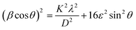
To investigate the strain effects that play a significant role in the GeS1−xSex alloys, we employed the Halder–Wagner (H–W) method, as described in Eqn (12), to quantify the strain contribution39,40:
| |
 | (12) |
where
β is the corrected full width at half maximum (FWHM, in radians),
θ is the Bragg angle,
D is the crystallite size,
ε is the strain value,
K is the shape factor (typically ∼0.9), and
λ is the X-ray wavelength.
Fig. 5d shows the strain values and crystallite size of GeS
1−xSe
x alloys as a function of Se content, calculated from the (
β/tan
θ)
2 versus β/tan
θsin
θ) plot (see Fig. S4). At low Se contents, the tensile stress increases with average crystallite size and reaches a maximum (
ε = 1.85 × 10
−2,
D = 367 Å) for the GeS
0.63Se
0.37 alloy (
x = 0.37). As the Se content becomes dominant, grain growth is significantly suppressed and does not increase again until the composition exceeds
x > 0.85. Notably, the
x = 0.61 composition shows the lowest residual stress (
ε = 0.89 × 10
−2) among the three Ge–S–Se systems. We attribute this trend to a composition-driven internal stress mechanism that operates differently across composition ranges. At low Se concentrations (
x = 0–0.37), stress along the van der Waals-dominated
a-axis is preferentially accommodated by interlayer sliding or delamination, whereas Se substitution correlates more strongly with lattice expansion along the
b- and
c-axes, consistent with previously reported observations.
35–38 This anisotropic lattice response is further supported by the larger deviation (bowing) from Vegard's law observed along the
b- and
c-axes (
Fig. 5a–c), indicating a more pronounced compositional dependence of lattice expansion in these directions. Although the strain values extracted from H–W analyses represent isotropically averaged microstrain, crystallographic anisotropy nevertheless offers a plausible framework to rationalize the observed increase in residual strain. The resulting localized lattice deformation generates intragranular stress that accumulates within larger grains, leading to increased tensile stress with increasing grain size.
41–43 At the intermediated-Se composition (
x = 0.37–0.61), the interfacial stress-relaxation effect is likely responsible for the strain reduction observed in the
x = 0.61 composition. These strain-disordered interfacial regions provide efficient pathways for stress release by enabling the redistribution and dissipation of deformation energy across the interfacial network. As these interfacial regions develop, the residual stress correspondingly decreases, alleviating stress concentrations and lowering the overall strain level.
44,45 As a result, the system tends to maintain smaller crystalline sizes to minimize the total free energy. At the rich-Se composition (
x = 0.61–0.85), the reintroduction of strain accommodation results in elevated intragranular stress (
ε = 1.17 × 10
−2). Such local stress enhances lattice distortion, reduces grain-boundary mobility, and consequently inhibits grain coarsening. At the Se-saturated regime (
x = 0.85 − 1), the lattice structure progressively converges toward that of pristine GeSe, which lowers the residual stress again and facilitates the slight coarsening of crystallites. These correlations between lattice size and tensile stress highlight the critical role of Se substitution in tuning the mechanical and structural behavior of GeS
1−xSe
x alloys.
To examine the influence of strain-induced lattice deformation in GeS1−xSex alloys, the deformation energy density was calculated based on the uniform deformation energy density model (UDEDM). Although this study introduces Vegard's law assumption, it may introduce some uncertainty in the absolute deformation energy values; however, we emphasize that the main conclusions of this work are based on the compositional trend of strain evolution, which remains valid regardless of the exact elastic modulus values (see supplementary page 6). Fig. 5e shows that both strain and deformation energy density reach their maximum at approximately x = 0.37, indicating the most severe lattice distortion and highest stored energy at this composition. With further increase in Se content, both parameters decrease markedly and eventually stabilize in the intermediate Se regime. The structure evolves into an energetically stabilized strain-disordered multi-interfacial crystalline configuration at x = 0.61 among the three Ge–S–Se compositions. Notably, the deformation energy density at x = 0.37 (22.84 × 10³ J m−3) is nearly 28 times higher than that at x = 0.61 (0.82 × 10³ J m−3), highlighting the pronounced strain accumulation at low composition of Se.
The dislocation density (δ ≈ 1/D2) was also evaluated, where δ denotes the dislocation density and D represents the crystallite size.46 Fig. 5f shows that in the low-Se composition range, the strain reaches its maximum while the δ concurrently drops to its minimum (0.74 line per Å2). This contrasting behavior suggests that the elevated strain originates primarily from accumulated lattice distortion, rather than from an increase in δ. In the intermediate Se composition regime, the residual stress decreases while the δ increases to 0.79 line per Å2. This trend likely stems from local mismatch strain that induces dislocation formation, together with partial structural loosening and the formation of strain-disordered interfacial regions that effectively dissipate residual stress. In the Se-rich composition range, both the residual stress and δ continue to increase, reaching 0.84 line per Å2 at x = 0.85. This rise originates from local lattice expansion, which generates heterogeneous distortions and strain-concentrated regions that promote dislocation formation. However, unlike the intermediate-Se regime, these dislocations cannot fully relieve the accumulated strain and instead introduce additional local distortions, leading to further residual stress—consistent with the slight increase in deformation energy density from 0.82 × 10³ to 1.66 × 10³ J m−3 between x = 0.61 and 0.85. At Se-saturated compositions (x = 0.85 − 1), lattice convergence toward the GeSe end-member diminishes internal stress and dislocation generation, yielding simultaneous declines in strain and δ.
We also determined the strain of the samples using the size–strain plot (SSP) method. This approach considers XRD peak broadening as arising from both size- and strain-induced contributions, as described in eqn (13)46:
| |
 | (13) |
where
dhkl is the interplanar spacing,
βhkl is the full width at half maximum (FWHM) of the diffraction peak (corrected for instrumental broadening, in radians),
θ is the Bragg angle,
K is the shape factor (0.9),
λ is the X-ray wavelength,
D is the average crystallite size, and
ε is the strain value. We plotted (
dhklβhklcos
θ)
2 versus (
dhkl2βhklcos
θ) to extract the strain and average crystallite size (see Fig. S5). Among the GeS
1−xSe
x series, the GeS
0.63Se
0.37 (
x = 0.37) sample exhibits the maximum tensile strain value of 2.86 × 10
−2, while the GeS
0.39Se
0.61 (
x = 0.61) sample shows the minimum tensile strain value of 1.37 × 10
−2 among the three Ge–S–Se compositions. The strain variation trend obtained from the SSP method closely aligns with that derived from the H–W analysis, as shown in
Fig. 6, confirming the reliability of both approaches in describing the strain evolution across compositions. Furthermore, the average crystallite size determined experimentally nearly coincides with that obtained from the H–W method, as illustrated in Fig. S6, indicating a strong correlation between the compositional variation and average crystallite size behavior in the alloy series. This consistency confirms that both methods reliably capture the evolution of tensile strain as the S-to-Se ratio changes, providing insights into the structural stabilization of the mixed alloy crystals. We have summarized the strain values, average crystallite sizes, deformation energy density and dislocation density values of the GeS
1−xSe
x alloys in
Table 2.
 |
| | Fig. 6 The comparison of the stress values obtained from the H–W and SSP methods. | |
Table 2 Comparison of the strain value, average crystallite size, deformation energy density, and dislocation density parameters of GeS1−xSex alloys
| Samples |
Strain values (H–W method) (×10−2) |
Strain values (SSP method) (×10−2) |
Average crystallite size (Å) |
Deformation energy density (×103 J m−3) |
Dislocation density (line per Å2) |
| GeS |
0.75 |
1.16 |
292 |
0.16 |
1.17 |
| GeS0.79Se0.21 |
1.08 |
1.66 |
327 |
2.07 |
0.94 |
| GeS0.63Se0.37 |
1.85 |
2.86 |
367 |
22.84 |
0.74 |
| GeS0.39Se0.61 |
0.89 |
1.37 |
356 |
0.82 |
0.79 |
| GeS0.15Se0.85 |
1.17 |
1.8 |
366 |
1.66 |
0.84 |
| GeSe |
0.96 |
1.48 |
345 |
0.28 |
0.75 |
To evaluate the structural stability after etching across the intermediate to Se-rich compositional regimes, both GeS0.39Se0.61 and GeS0.15Se0.85 samples were subjected to HF (9.5%) acid etching for 20 seconds. Fig. 7a and b SEM images reveal that GeS0.39Se0.61 exhibits a porous surface morphology, while GeS0.15Se0.85 maintains a relatively localized and step-like etched surface. This difference can be attributed to the higher density of strain-disordered interfacial regions in the GeS0.39Se0.61 sample, which exhibit elevated interfacial energy and chemical reactivity,47,48 rendering them more susceptible to preferential attack during the etching process. The dissolution or removal of material along these interfaces leaves voids or grooves between adjacent grains. In contrast, the step-like surface of GeS0.15Se0.85 is formed through layer-by-layer etching along specific intragranular crystal planes. These results reveal that under the respective dominance of intragranular and interfacial stress-relaxation effects, the etching process displays orientation-dependent rates, thereby giving rise to different etching characteristics. Significantly, the porous structure usually offers multiple advantages, including an increased active site and improved charge transport for electrochemical applications.49
 |
| | Fig. 7 SEM images of (a) GeS0.39Se0.61 and (b) GeS0.15Se0.85 samples after HF etching. | |
To evaluate the optical bandgap (Eg) of the GeS1−xSex crystals with varying Se contents, their absorption spectra were recorded at room temperature. Near the band edge, the optical absorption characteristics of a semiconductor can be approximately described by eqn (14)50:
| |
 | (14) |
Here,
α denotes the absorption coefficient, which is proportional to the absorbance (
α),
Eph represents the photon energy,
Eg is the optical bandgap,
C is a proportionality constant, and
n is an exponent characterizing the nature of the interband transition (
n = 2 for direct and
n = 1/2 for indirect transitions). Fig. S7(a–f) exhibit a pronounced two-step absorption profile, revealing the presence of two distinct optical transitions, denoted as
E1 and
E0. Among the alloy series, only the GeS
0.79Se
0.21 sample does not exhibit two distinct energy plateaus; therefore, the second bandgap must be identified through polarization-dependent measurements (see Fig. S7b). The transition energies
E1 and
E0 were determined by extrapolating the linear regions of the (
αEph)
2 and (
αEph)
1/2 plots to zero, corresponding to the armchair and zigzag directions, respectively.
51,52 Based on these analyses,
Fig. 8a and b illustrate the dependence of
Eindg and
Edirg on the Se content, respectively. The direct bandgaps of GeS, GeS
0.79Se
0.21, GeS
0.63Se
0.37, GeS
0.39Se
0.61, GeS
0.15Se
0.85, and GeSe samples were determined to be approximately 1.60 eV, 1.50 eV, 1.43 eV, 1.35 eV, 1.23 eV, and 1.15 eV respectively. The indirect bandgaps of GeS, GeS
0.79Se
0.21, GeS
0.63Se
0.37, GeS
0.39Se
0.61, GeS
0.15Se
0.85, and GeSe samples were determined to be approximately 1.59 eV, 1.49 eV, 1.42 eV, 1.33 eV, 1.21 eV, and 1.13 eV. Both bandgaps exhibit a redshift with increasing
x. This behavior arises from the substitution of S atoms by the larger Se atoms, which expands the lattice constants and consequently reduces the bandgap energies. These results are in good agreement with previously reported values, confirming the reliability of our optical bandgap evaluation, as summarized in
Table 3.
 |
| | Fig. 8 (a) Tauc plots of (αEph)2 and (b) (αEph)1/2 versus photon energy (Eph) for evaluating the direct and indirect optical bandgaps, respectively. (c) The evolution of the direct and indirect bandgaps, following Vegard's law as a function of Se content. (d) The variation of electrical resistivity of GeS1−xSex alloys as a function of Se content. | |
Table 3 Room-temperature bandgaps of GeS1−xSex (0 ≤ x ≤ 1) crystals from this work and literature reports
| Materials |
Evaluated band gaps |
Eg (eV) |
Ref. |
| GeS |
Diffuse reflectance spectra |
1.6 eV (direct) |
56 |
| GeSe |
1.2 eV (direct) |
| GeSe |
Photoluminescence spectroscopy |
1.16 ± 0.13 eV (direct) |
29 |
| GeS0.5Se0.5 |
Absorption spectra |
1.28 (indirect), 1.58 (direct) |
22 |
| GeS |
Cathodoluminescence spectroscopy |
1.6 eV (indirect) |
53 |
| GeS0.46Se0.54 |
1.36 eV (indirect) |
| GeSe |
1.27 eV (indirect) |
| GeS |
Absorption spectra |
1.65 (direct) |
15 |
| GeS0.73Se0.27 |
1.57 (direct) |
| GeS0.42Se0.58 |
1.45 (direct) |
| GeS0.29Se0.71 |
1.39 (direct) |
| GeSe |
1.14 (direct) |
| GeS |
Absorption spectra |
1.59 (indirect), 1.60 (direct) |
This study |
| GeS0.79Se0.21 |
1.49 (indirect), 1.50 (direct) |
| GeS0.63Se0.37 |
1.42 (indirect), 1.43 (direct) |
| GeS0.39Se0.61 |
1.33 (indirect), 1.35 (direct) |
| GeS0.15Se0.85 |
1.21 (indirect), 1.23 (direct) |
| GeSe |
1.13 (indirect), 1.15 (direct) |
In general, the bandgap of a mixed crystal shows a quadratic dependence on composition. Thus, the variation of Eg with x in GeS1−xSex can be described by the following Vegard's law in eqn (15):50
| | |
Eg(x) = (1 − x)Eg,GeS + xEg,GeSe
| (15) |
Here,
Eg,
GeS and
Eg,GeSe denote the bandgaps of pure GeS and GeSe, respectively. By fitting
eqn (15) to the experimental results of
Eindg and
Edirg.
Fig. 8c shows that the low-Se compositions closely follow Vegard's law, while the moderate to Se-rich regime exhibits a slight upward deviation. We infer that in the low-Se regime, the lattice framework remains largely GeS-like, resulting in near-linear strain evolution, and consequently a bandgap trend that closely follows Vegard's law. In contrast, in the moderate to Se-rich regime, residual Ge–S bonds, local bond-length fluctuations, and incomplete convergence of the VBM/CBM
k-points persist despite overall strain relaxation, thereby slowing the bandgap reduction. This deviation is consistent with the asymmetric bandgap bowing commonly observed in chalcogenide alloys.
53,54 Furthermore, as
x approaches 1 (GeSe), the
Eindg and
Edirg converge, with both curves becoming nearly identical, indicating a transition toward quasi-direct-gap behavior. This trend shows a strong resemblance to the phenomenon previously reported by our group in CVT-grown GaS
1−xSe
x alloys.
50 Consequently, these bandgap-tunable alloys present significant opportunities for advanced optoelectronic applications.
The current–voltage (I–V) characteristic curve represents one of the most fundamental electrical properties of a semiconductor material. In this experiment, we connected the crystals to electrodes with identical spacing and measured their I–V responses. Fig. S8 presents the I–V curves of GeS, GeSe, and the ternary GeS1−xSex alloy series. By applying Ohm's law (V = I × R),55 we determined that the resistivity values of GeS, GeS0.79Se0.21, GeS0.63Se0.37, GeS0.39Se0.61, GeS0.15Se0.85, and GeSe are 34.46 Ω m, 52.71 Ω m, 25.07 Ω m, 12.9 Ω m, 0.44 Ω m, and 0.144 Ω m, respectively. These results clearly show that, at a fixed bias voltage of 5 V, the electrical current increases with increasing Se content, with the GeSe crystal exhibiting the highest conductivity among all samples. However, the GeS0.79Se0.21 (x = 0.21) sample displays an anomalously high resistivity. This anomaly likely arises from the competition between defect-induced carrier scattering and intrinsic band structure evolution. At low Se substitution levels, local lattice distortion and defect formation caused by Ge–S/Ge–Se bonding mismatch enhance carrier scattering, thereby increasing resistivity. With further Se incorporation, bandgap narrowing and the associated increase in carrier concentration gradually become dominant. At x = 0.37, where the deformation energy density reaches its maximum while the resistivity decreases, this apparent discrepancy can be tentatively interpreted within the classical transport relationship ρ = 1/(qnμ), in which resistivity (ρ) is inversely proportional to the carrier concentration (n) and carrier mobility (μ).57 Although defect- and strain-induced scattering tends to reduce μ, a sufficiently large increase in n resulting from alloying-induced bandgap narrowing can compensate for the mobility loss and even lead to a net reduction in resistivity. Therefore, the decreasing resistivity at x = 0.37 is consistent with a carrier-density-dominated transport regime, where bandgap-narrowing-induced carrier generation outweighs the mobility reduction from enhanced defect scattering. This compositional dependence of conductivity reflects the gradual electronic structure evolution induced by S → Se substitution. The reduction in bandgap and the enhanced orbital overlap between Ge–Se bonds facilitate carrier transport, thereby improving the overall electrical performance of the GeS1−xSex alloy system.
4. Conclusions
In summary, GeS1−xSex (0 ≤ x ≤ 1) alloys were successfully synthesized via CVT, forming a continuous composition between GeS and GeSe. The H–W and SSP analyses consistently show that the strain analysis of GeS1-xSex alloys reveals four distinct compositional regimes. At low Se contents, both strain and deformation energy density reach a maximum around x = 0.37, suggesting severe lattice distortion and significant energy accumulation in the low-Se composition range. In the intermediate Se range, strain relaxation becomes dominant, accompanied by a reduction in crystallite size. The observed relaxation behavior at x = 0.61 is attributed to the formation of a strain-disordered crystalline structure with abundant interfacial regions, which acts as an effective strain-buffering network. This structure allows deformation energy to dissipate across strain-disordered interfacial regions, alleviating interfacial stress concentrations and improving structural stability. Consequently, the system attains a lower overall strain state and enhanced thermodynamic stability. In the Se-rich regime, renewed lattice expansion and heterogeneous distortion regenerate localized misfit strain, increasing both residual stress and dislocation density. As the Se content approaches saturation (x = 0.85 − 1), the structure no longer generates a substantial number of defects. These results confirm that selenium substitution not only governs anisotropic lattice deformation but also facilitates strain redistribution through interfacial relaxation, ultimately tuning the mechanical and microstructural behavior of GeS1−xSex alloys. Optical measurements demonstrated a tunable redshift in direct and indirect bandgaps from 1.60 eV (GeS) to 1.15 eV (GeSe), attributable to lattice expansion and orbital hybridization. Electrical testing revealed a corresponding reduction in resistivity from 34.46 Ω m to 0.144 Ω m with increasing Se content, indicating improved carrier transport. Collectively, the composition-dependent bandgap tunability, strain-modulated structural evolution, and the resulting regulation of electrical transport properties demonstrated in this work provide important design guidelines for anisotropic IV–VI layered semiconductors. Such characteristics make GeS1−xSex alloys promising for applications in polarization-sensitive photodetectors, infrared optoelectronics, and strain- and composition-engineered electronic and optoelectronic devices, where simultaneous control of optical response and electrical conductivity is desired.
Conflicts of interest
There are no conflicts to declare.
Data availability
The data that support the findings of this study are available from the corresponding author upon reasonable request.
The Supporting information includes structural, optical, and electrical characterization of GeS1−xSex alloys. Data are available from the corresponding author upon reasonable request. See DOI: https://doi.org/10.1039/d6tc00046k.
Acknowledgements
This work was supported by the National Science and Technology Council (NSTC) of the Republic of China under grant numbers NSTC 114–2222-E-018–003 and NSTC 114–2221-E-018–013.
References
- A. K. Tołłoczko, S. J. Zelewski, J. Ziembicki and N. Olszowska, Photoemission Study of the Thermoelectric Group IV-VI van der Waals Crystals (GeS, SnS, and SnSe), Adv. Opt. Mater., 2024, 12, 2302049, DOI:10.1002/adom.202302049.
- C. Wang, X. Shi, S. Liu, H. Zhao and W. Zhang, Preparation of Mixed Few-Layer GeSe Nanosheets with High Efficiency by the Thermal Sublimation Method, ACS Appl. Mater. Interfaces, 2023, 15, 39732–39739, DOI:10.1021/acsami.3c08027.
- A. Tołłoczko, S. J. Zelewski, M. Błaszczak, A. Siudzin and R. Kudrawiec, Optical properties of orthorhombic germanium selenide: an anisotropic layered semiconductor promising for optoelectronic applications, J. Mater. Chem. C, 2021, 14838–14847, 10.1039/d1tc04280g.
- P. T. Bui, V. Van On, J. Guerrero-Sanchez and D. M. Hoat, Electronic and magnetic properties of GeS monolayer effected by point defects and doping, RSC Adv., 2024, 14, 2481–2490, 10.1039/d3ra07942b.
- E. Sutter, J. S. French and P. Sutter, Tunable Layer Orientation and Morphology in Vapor-Liquid-Solid Growth of One-Dimensional GeS van der Waals Nanostructures, Chem. Mater., 2021, 33, 3980–3988, DOI:10.1021/acs.chemmater.1c00289.
- J. Zhao, Z. Zhao, Z. Song and M. Zhu, GeSe ovonic threshold switch: the impact of functional layer thickness and device size, Sci. Rep., 2024, 14, 6685, DOI:10.1038/s41598-024-57029-7.
- Z. Q. Fan, X. W. Jiang, Z. Wei, J. W. Luo and S. S. Li, Tunable Electronic Structures of GeSe Nanosheets and Nanoribbons, J. Phys. Chem. C, 2017, 121, 14373–14379, DOI:10.1021/acs.jpcc.7b04607.
- J. J. Wang, Y. F. Zhao, J. D. Zheng, X. T. Wang, X. Deng, Z. Guan, R. R. Ma, N. Zhong, F. Y. Yue, Z. M. Wei, P. H. Xiang and C. G. Duan, Strain-engineering on GeSe: Raman spectroscopy study, Phys. Chem. Chem. Phys., 2021, 23, 26997–27004, 10.1039/d1cp03721h.
- Y. Shi, M. Yuan, M. Wei, Y. Wang, M. Qin, Z. Wei, Y. Chen and J. Lian, Physica B: Condensed Matter Thickness modulated optical and bandgap properties at visible frequencies of GeSe thin films, Phys. B, 2025, 705, 417085, DOI:10.1016/j.physb.2025.417085.
- I. Seo and S. W. Martin, Fast lithium ion conducting solid state thin-film electrolytes based on lithium thio-germanate materials, Acta Mater., 2011, 59, 1839–1846, DOI:10.1016/j.actamat.2010.11.050.
- X. Hu, P. Huang, K. Liu, B. Jin, X. Zhang, X. Zhang, X. Zhou and T. Zhai, Salt-Assisted Growth of Ultrathin GeSe Rectangular Flakes for Phototransistors with Ultrahigh Responsivity, ACS Appl. Mater. Interfaces, 2019, 26, 23353–23360, DOI:10.1021/acsami.9b06425.
- J. Qu, C. Liu, M. Zubair, Z. Zeng, B. Liu, X. Yang, Z. Luo, X. Yi, Y. Chen, S. Chen and A. Pan, A universal growth method for high-quality phase-engineered germanium chalcogenide nanosheets, Nanoscale, 2023, 15, 4438–4447, 10.1039/d2nr05657g.
- Q. Wu, X. Pan, W. Zhao, Y. Gao, D. Zhao, S. Yan, T. Li, F. Miao, Z. Fei and Y. Shi, Twisted GeS Nanowire with Engineered Stacking Order and Tunable Composition, Adv. Mater. Interfaces, 2025, 12, 2400802, DOI:10.1002/admi.202400802.
- E. Sutter and P. Sutter, Self-Assembly of Mixed-Dimensional GeS1−xSex (1D Nanowire)– (2D Plate) van der Waals Heterostructures, Small, 2023, 19, 1–8, DOI:10.1002/smll.202302592.
- T. Zheng, Y. Pan, M. Yang, Z. Li, Z. Zheng, L. Li, Y. Sun, Y. He, Q. Wang, T. Cao, N. Huo and Z. Chen, 2D Free-Standing GeS1−xSex with Composition-Tunable Bandgap for Tailored Polarimetric Optoelectronics, Adv. Mater., 2024, 36, 2313721, DOI:10.1002/adma.202313721.
- S. Liu, Q. Ma, C. Lin, C. Hong, R. Yi, R. Wang, R. Li, X. Liu, A. Nie, X. Gan, Y. Cheng and W. Huang, Alloy engineered germanium monochalcogenide with tunable bandgap for broadband optoelectrical applications, Phys. Rev. Mater., 2020, 4, 074012, DOI:10.1103/PhysRevMaterials.4.074012.
- E. Sutter, K. Kisslinger, R. R. Unocic, K. Burns, J. Hachtel and P. Sutter, Photonics in Multimaterial Lateral Heterostructures Combining Group IV Chalcogenide van der Waals Semiconductors, Small, 2024, 20, 2307372, DOI:10.1002/smll.202307372.
- S. C. Liu, Y. Yang, X. Zhang, L. B. Huang, J. K. Sun, B. Guan, X. Li, D. J. Xue and J. S. Hu, Tuning the Optical Absorption Property of GeSe Thin Films by Annealing Treatment, Phys. Status Solidi RRL, 2018, 12, 1800370, DOI:10.1002/pssr.201800370.
- M. Binnewies, R. Glaum, M. Schmidt and P. Schmidt, Chemical vapor transport reactions, Chemical Vapor Transport Reactions, 2021, pp. 1–628 DOI:10.1515/9783110254655.
- A. Y. Zavrazhnov, I. D. Zartsyn, D. N. Turchen, A. V. Naumov and V. P. Zlomanov, Chemical vapor transport as a means of controlling the composition of condensed phases, Inorg. Mater., 2004, 40, S101–S127, DOI:10.1007/s10789-005-0056-6.
- Z. Fang, Y. Liu, S. Gee, S. Lin, S. Koyama, C. So, F. Luo, R. Chen, B. Tang and J. Yao, Chemically Modulating the Twist Rate of Helical van der Waals Crystals, Chem. Mater., 2020, 32, 299–307, DOI:10.1021/acs.chemmater.9b03779.
- S. Unadkat, G. K. Solanki and M. Tannarana, A study of optical band gap in GeS1−xSex (x = 0,0.5,1) single crystals grown using chemical vapour transport technique, Pramana – J. Phys., 2021, 95, 83, DOI:10.1007/s12043-021-02105-0.
- A. Y. Zavrazhnov, I. D. Zartsyn, D. N. Turchen, A. V. Naumov and V. P. Zlomanov, Chemical vapor transport as a means of controlling the composition of condensed phases, Inorg. Mater., 2004, 40, S101–S127, DOI:10.1007/s10789-005-0056-6.
- M. Binnewies, R. Glaum, M. Schmidt and P. Schmidt, Chemical Vapor Transport Reactions, Walter de Gruyter GmbH & Co. KG, Berlin/Boston, 2012 Search PubMed.
- Y. Mao, N. Chen, T. Deng and Z. Lan, Two-dimensional GeS synthesized by one-step space-confined APCVD and its self-powered photodetector, Phys. B, 2024, 685, 415984, DOI:10.1016/j.physb.2024.415984.
- Y. Liu, M. Sun, G. Tang, G. Qian, W. Liu, Z. Shi, W. Zhu, Q. Qian, S. Xu and Z. Yang, Multifunctional GeSe core fibers, Mater. Lett., 2019, 247, 193–196, DOI:10.1016/j.matlet.2019.03.124.
- X. Wu, F. Yuan, M. Yang, P. Jiang, C. Zhang, L. Chen, Y. Wei and E. Ma, Nanodomained nickel unite nanocrystal strength with coarse-grain ductility, Sci. Rep., 2015, 5, 11728, DOI:10.1038/srep11728.
- M. R. Mohammadzadeh, A. Hasani, K. Jaferzadeh, M. Fawzy, T. De Silva, A. Abnavi, R. Ahmadi, H. Ghanbari, A. Askar, F. Kabir, R. K. N. D. Rajapakse and M. M. Adachi, Unique Photoactivated Time-Resolved Response in 2D GeS for Selective Detection of Volatile Organic Compounds, Adv. Sci., 2023, 10, 1–10, DOI:10.1002/advs.202205458.
- H. Zhao, Y. Mao, X. Mao, X. Shi, C. Xu, C. Wang, S. Zhang and D. Zhou, Band Structure and Photoelectric Characterization of GeSe Monolayers, Adv. Funct. Mater., 2018, 28, 1–10, DOI:10.1002/adfm.201704855.
- J. J. Wang, Y. F. Zhao, J. D. Zheng, X. T. Wang, X. Deng, Z. Guan, R. R. Ma, N. Zhong, F. Y. Yue, Z. M. Wei, P. H. Xiang and C. G. Duan, Strain-engineering on GeSe: Raman spectroscopy study, Phys. Chem. Chem. Phys., 2021, 23, 26997–27004, 10.1039/d1cp03721h.
- P. Sutter, H. Komsa, K. Kisslinger and E. Sutter, Lateral Integration of SnS and GeSe van der Waals Semiconductors: Interface Formation, Electronic Structure, and Nanoscale Optoelectronics, ACS Nano, 2023, 17(10), 9552–9564, DOI:10.1021/acsnano.3c02411.
- Y. Mao, N. Chen, T. Deng and Z. Lan, Two-dimensional GeS synthesized by one-step space-confined APCVD and its self-powered photodetector, Phys. B, 2024, 685, 415984, DOI:10.1016/j.physb.2024.415984.
- Z. Chen, W. Hwang, M. Cho, A. T. Hoang, M. Kim, D. Kim, D. H. Kim, Y. D. Kim, H. J. Kim, J. H. Ahn, A. Soon and H. J. Choi, In-plane optical and electrical anisotropy in low-symmetry layered GeS microribbons, NPG Asia Mater., 2022, 14, 41, DOI:10.1038/s41427-022-00390-8.
- H. Giefers and M. Nicol, High pressure X-ray diffraction study of all Fe-Sn intermetallic compounds and one Fe-Sn solid solution, J. Alloys Compd., 2006, 422, 132–144, DOI:10.1016/j.jallcom.2005.11.061.
- L. Li, C. Feng and J. Yang, Tensile and compressive behaviors of prestrained single-layer black phosphorus: A molecular dynamics study, Nanoscale, 2017, 9, 3609–3619, 10.1039/c6nr09763d.
- L. Li and J. Yang, On mechanical behaviors of few-layer black phosphorus, Sci. Rep., 2018, 8, 3227, DOI:10.1038/s41598-018-21633-1.
- M. H. Rahman, S. Mitra, M. Motalab and P. Bose, Investigation on the mechanical properties and fracture phenomenon of silicon doped graphene by molecular dynamics simulation, RSC Adv., 2020, 10, 31318–31332, 10.1039/d0ra06085b.
- Y. Sun, Y. Wang, E. Wang, B. Wang, H. Zhao, Y. Zeng, Q. Zhang, Y. Wu, L. Gu, X. Li and K. Liu, Determining the interlayer shearing in twisted bilayer MoS2 by nanoindentation, Nat. Commun., 2022, 13, 3898, DOI:10.1038/s41467-022-31685-7.
- M. K. Alam, M. S. Hossain, N. M. Bahadur and S. Ahmed, A comparative study in estimating of crystallite sizes of synthesized and natural hydroxyapatites using Scherrer Method, Williamson-Hall model, Size-Strain Plot and Halder-Wagner Method, J. Mol. Struct., 2024, 1306, 137820, DOI:10.1016/j.molstruc.2024.137820.
- M. K. Alam, M. S. Hossain, M. S. Islam, N. M. Bahadur and S. Ahmed, Sustainable synthesis and characterization of nano-triple superphosphate from solid marine wastes, Mater. Adv., 2024, 5, 6618–6629, 10.1039/d4ma00513a.
- X. Li, B. Ma, B. Liu, L. Li, J. Cao and C. Xu, Study on the mechanism of grain size and residual stress coupling distribution on the intergranular corrosion susceptibility of AZ31B magnesium alloy, RSC Adv., 2024, 14, 38832–38854, 10.1039/d4ra07164f.
- A. Gupta, J. Gruber, S. S. Rajaram, G. B. Thompson, D. L. McDowell and G. J. Tucker, On the mechanistic origins of maximum strength in nanocrystalline metals, NPJ Comput. Mater., 2020, 6, 153, DOI:10.1038/s41524-020-00425-0.
- M. J. Chen, D. Xie, S. Fensin, A. Hunter, N. Li and M. A. Zikry, Intergranular fracture, grain-boundary structure, and dislocation-density interactions in FCC bicrystals, Sci. Rep., 2024, 14, 2011, DOI:10.1038/s41598-024-72033-7.
- F. Banhart, Strains in crystals with amorphous surface films studied by convergent beam electron diffraction and high-resolution imaging, Ultramicroscopy, 1994, 56, 233–240, DOI:10.1016/0304-3991(94)90011-6.
- Z. Pan and T. J. Rupert, Amorphous intergranular films as toughening structural features, Acta Mater., 2015, 89, 205–214, DOI:10.1016/j.actamat.2015.02.012.
- M. Basak, M. L. Rahman, M. F. Ahmed, B. Biswas and N. Sharmin, The use of X-ray diffraction peak profile analysis to determine the structural parameters of cobalt ferrite nanoparticles using Debye-Scherrer, Williamson-Hall, Halder-Wagner and Size-strain plot: Different precipitating agent approach, J. Alloys Compd., 2022, 895, 162694, DOI:10.1016/j.jallcom.2021.162694.
- Y. Guo, Y. Xu and P. Chen, Ampere-level glycerol electrooxidation enabled by oxygen vacancy-riched crystalline/amorphous Co3O4-x/ZrO2-x Heterointerface, J. Colloid Interface Sci., 2025, 699, 138292, DOI:10.1016/j.jcis.2025.138292.
- Y. Long, X. Zhu, C. Gao, W. Si, J. Li and Y. Peng, Modulation of Co spin state at Co3O4 crystalline-amorphous interfaces for CO oxidation and N2O decomposition, Nat. Commun., 2025, 16, 1048, DOI:10.1038/s41467-025-56487-5.
- O. Okhay and A. Tkach, A comprehensive review of the use of porous graphene frameworks for various types of rechargeable lithium batteries, J. Energy Storage, 2024, 80, 110336, DOI:10.1016/j.est.2023.110336.
- Y. Shih, D. Lin, B. Tseng, Y. Kao, S. Hwang and C. Lin, Structural and optical characterization of GaS1−xSex layered mixed crystals grown by chemical vapor transport, Mater. Today Commun., 2023, 37, 107047, DOI:10.1016/j.mtcomm.2023.107047.
- A. Tołłoczko, R. Oliva, T. Woźniak, J. Kopaczek, P. Scharoch and R. Kudrawiec, Anisotropic optical properties of GeS investigated by optical absorption and photoreflectance, Mater. Adv., 2020, 1, 1886–1894, 10.1039/d0ma00146e.
- A. Tołłoczko, S. J. Zelewski, M. Błaszczak, T. Woźniak, A. Siudzińska, A. Bachmatiuk, P. Scharoch and R. Kudrawiec, Optical properties of orthorhombic germanium selenide: an anisotropic layered semiconductor promising for optoelectronic applications, J. Mater. Chem. C, 2021, 9, 14838–14847, 10.1039/d1tc04280g.
- E. Sutter, H.-P. Komsa, J. S. French, P. Sutter, A. Paragon and P. Environment, Composition Dependence of the Band Gaps of Semiconducting GeSxSe1-x van der Waals Alloys, Chem. Mater., 2023, 35, 6374–6381, DOI:10.1021/acs.chemmater.3c01069.
- J. Yu, C. Y. Xu, Y. Li, F. Zhou, X. S. Chen, P. A. Hu and L. Zhen, Ternary SnS2-x Sex Alloys Nanosheets and Nanosheet Assemblies with Tunable Chemical Compositions and Band Gaps for Photodetector Applications, Sci. Rep., 2015, 5, 17109, DOI:10.1038/srep17109.
- D. D. Vaughn, R. J. Patel, M. A. Hickner and R. E. Schaak, Single-crystal colloidal nanosheets of GeS and GeSe, J. Am. Chem. Soc., 2010, 132, 15170–15172, DOI:10.1021/ja107520b.
- P. Ramasamy, D. Kwak, D.-H. Lim, H.-S. Ra and J.-S. Lee, Solution synthesis of GeS and GeSe nanosheets for high-sensitivity photodetectors, J. Mater. Chem. C, 2016, 4, 479–485, 10.1039/C5TC03667D.
- M. Takashiri, T. Shirakawa, K. Miyazaki and H. Tsukamoto, Fabrication and characterization of Bi0.4Te3.0Sb1.6 thin films by flash evaporation method, J. Alloys Compd., 2007, 441, 246–250, DOI:10.1016/j.jallcom.2006.09.136.
|
| This journal is © The Royal Society of Chemistry 2026 |
Click here to see how this site uses Cookies. View our privacy policy here. 
 Open Access Article
 This Open Access Article is licensed under a Creative Commons Attribution-Non Commercial 3.0 Unported Licence
 *b
*b


