DOI:
10.1039/D5TC03985A
(Review Article)
J. Mater. Chem. C, 2026,
14, 2555-2586
Research progress in double perovskite oxide half-metals for magnetic storage technology
Received
9th November 2025
, Accepted 21st January 2026
First published on 23rd January 2026
Abstract
With the development of spintronics and magnetic storage technologies towards ultra-high density, ultra-low power consumption, and ultra-fast response, double perovskite oxide half-metals (DPOHMs) have become core candidate materials to break through the performance bottlenecks of traditional magnetic storage devices due to their tunable crystal structure, high Curie temperature (Tc), nearly 100% spin polarization (SP), and excellent chemical stability. Here, we systematically review the research progress in DPOHMs used for magnetic storage devices, which covers crystal structure regulation, microstructural characterization, physical property characterization methods, theoretical calculation models, and their applications in magnetic storage devices. Firstly, synthesis methods (sol–gel methods, pulsed laser deposition, magnetron sputtering, etc.) and structural characterization of DPOHMs are described, and the effects of A-/B-site element doping and oxygen vacancy regulation on the crystal ordering degree and half-metallic properties are analyzed. Then, the correlation between microstructures and material properties is critically discussed. In addition, theoretical investigations into the physical origins of the half-metallicity of DPOHMs by first-principles calculations (density functional theory (DFT) plus the U method (DFT+U)) are critically reviewed, especially the theoretical simulations of band structures, density of states, magnetic exchange interactions, and defect effects. Finally, the promising applications of DPOHMs in magnetic tunnel junctions, spin valves, and spin field-effect transistors are systematically summarized, and the current challenges and future prospects of DPOHMs in the field of magnetic storage are discussed.

Qingkai Tang
| Qingkai Tang is currently a lecturer at Shandong Police University, specializing in condensed matter physics. In 2024, he received his PhD in Physics from Nanjing University, Nanjing, China and MS degree from Northwestern Polytechnical University, Xi'an, China. His present work focuses on the synthesis and structural characterization of double perovskite oxide nanostructures and their applications in the fields of electrocatalysis, photovoltaics, and spintronics. |

Xinhua Zhu
| Xinhua Zhu is currently a full professor at Nanjing University. He received his BS (1989), MS (1992), and PhD (1995) degrees in Electronic Materials Science from Xi’an Jiaotong University, Xi'an, China. He worked as an academic consultant at the King Abdullah University of Science & Technology (KAUST, Kingdom of Saudi Arabia) in 2012 and 2013, Queen's University of Belfast (United Kingdom) from 2004 to 2006, Max-Planck-Inst Mikrostrukturphys (Halle, Germany) from 2003 to 2004, and The Hong Kong Polytechnic University from 2000 to 2001. His current research interests cover nanoscale fabrication of multiferroic (double) perovskite nanostructures and their structural characterization by (HR)TEM techniques. |
1. Introduction
With the explosive development of fields such as 5G, artificial intelligence, and police big data, the global demand for data storage doubles every two years. Traditional hard disk drives (HDD) and Not AND (NAND) flash memory can hardly meet the requirements of next-generation storage for “Tb-level density, sub-ns-level speed, and sub-fJ-level energy efficiency”.1,2 High spin polarization (SP) materials are essential for overcoming the performance constraints of conventional devices, which are being replaced by spintronic devices due to their “non-volatility, low power consumption, and high integration”.3,4 Half-metallic materials are considered as “ideal electrode materials” for spintronic devices because of their special electronic structure of “metallicity in one spin channel and insulation in the other spin channel” at the Fermi level, which permits them to provide 100% spin-polarized current.5,6
Among numerous half-metallic systems, double perovskite oxides with the general chemical formula A2BB′O6 (where A is an alkaline earth/rare earth metal and B/B′ are transition metals) have special advantages: (1) structural flexibility: the electronic structure and magnetic ordering can be precisely regulated via A-site and B-site element doping (e.g., Sr2+/La3+ substitution at the A-site and Co3+/Ni2+ doping at the B-site);7,8 (2) room-temperature (RT) stability: the Curie temperature (TC) of typical systems such as Sr2FeMoO6 (SFMO) reaches 420–480 K, which far exceeds RT;9,10 (3) oxide compatibility: they have a high lattice matching degree with insulating barrier layers such as MgO and Al2O3, which can reduce interface scattering loss.11,12 Ever since Kobayashi et al. first reported the half-metallicity and tunnel magnetoresistance (TMR) effect of SFMO in 1998,13 research studies on double perovskite oxide half-metals (DPOHMs) have expanded from a single system to multi-element doping, heterostructure construction, and device integration.14,15
However, the practical applications of DPOHMs still face three core issues: (1) from the microstructural view, the low ordering degree of B/B′-site atoms and numerous oxygen vacancy defects lead to the deviation of spin polarization from the theoretical value;16,17 (2) from the physical property view, insufficient magnetic anisotropy energy (MAE) and fast magnetic moment relaxation at high temperatures affect the thermal stability of devices;18,19 and (3) from the aspect of theory–experiment deviation, a difference exists between the predicted values by first-principles and the experimental ones, requiring more accurate calculation models.20,21
In order to develop high-performance magnetic storage devices, in this review the mechanisms underlying the correlation between the structure, performance, and applications of DPOHMs are critically analysed from three aspects: microstructural characterization, physical property measurements, and theoretical calculations, and more research perspectives for DPOHMs are also pointed out. For more details, this review is arranged as the following. We briefly introduce the fundamental crystal structures of DPOHMs and their synthesis methods, followed by their microstructural and physical property characterization. Then, theoretical calculation models (such as density functional theory (DFT) plus the U method (DFT+U) and GW approximation) for band structures and defect effect simulation are described. Finally, the applications of DPOHMs in the fields of magnetic tunnel junctions (MTJs), spin valves, and spin field-effect transistors are critically discussed, and the challenges and prospects associated with developing DPOHMs are also presented.
2 Crystal structure and synthesis methods of DPOHMs
2.1 Crystal structure characteristics and the origin of half-metallicity
The perovskite ABO3 structure serves as the basis for the crystal structure of DPOHMs. B/B′ ions occupy the octahedral interstitial positions in A2BB′O6 in either an orderly or disordered manner. It can be classified into the following categories based on the arrangement symmetry of B/B′ ions: (i) rock-salt type ordering (Fm![[3 with combining macron]](https://www.rsc.org/images/entities/char_0033_0304.gif) m space group) in which B and B′ ions alternately occupy the (0, 0, 0) and (0.5, 0.5, 0.5) locations;13,22 (ii) disordered structure (Pmm space group) where B and B′ ions are dispersed randomly, and half-metallicity tends to vanish; and (iii) layered ordering (P4/mmm space group) where B and B′ ions are stacked in layers along the c-axis, such as La2CoMnO6 (LCMO).23,24
m space group) in which B and B′ ions alternately occupy the (0, 0, 0) and (0.5, 0.5, 0.5) locations;13,22 (ii) disordered structure (Pmm space group) where B and B′ ions are dispersed randomly, and half-metallicity tends to vanish; and (iii) layered ordering (P4/mmm space group) where B and B′ ions are stacked in layers along the c-axis, such as La2CoMnO6 (LCMO).23,24
The nature of half-metallicity lies in electron spin–orbit coupling (SOC) and exchange splitting: the d-orbitals of B/B′ ions hybridize with the p-orbitals of O2−, forming a spin-up conduction band (metallic) and a spin-down bandgap (insulating).5,25 For example, in the calculated electron band structures of Ca2TiRuO6 HM DP oxides by GGA and GGA+U methods, a bandgap near the Fermi level with a value of 1.30 eV is observed for the up-spin polarization, as depicted in Fig. 1(a), which allows the material to be classified as semiconducting for up-spin orientation. On the other hand, for down-spin polarization (Fig. 1(b)), the bands closer to the Fermi level pass through it as expected in conducting materials.26 This type of behaviour, non-conducting for one spin orientation and conducting for the other, is characteristic of so-called HM materials.27 The semiconducting nature in up-spin orientation originates from the d–p hybridization between Ti-3d and O-2p orbitals, which takes place in the TiO6 octahedra, while the conducting characteristic in down-spin orientation is ascribed to d–p hybridization between Ru-4d and O-2p orbitals in the RuO6 octahedra. This is confirmed by the total DOS in Ca2TiRuO6 (Fig. 1c) and partial DOS contributed by Ti-3d, Ru-4d, and O-p orbitals for the spin-up and spin-down configurations, as illustrated in Fig. 1(c)–(f). When comparing the total and partial DOS between the two calculation procedures with GGA and GGA+U, it is noticed that the inclusion of the correction potential U causes a shift of the electronic orbitals towards states further away from the Fermi level, both in the valence band and in the conduction band, which consequently expands the bandgap values from 1.30 eV to 1.56 eV (seen in Fig. 1(a)), with an average between up and down cannels of 0.78 eV. This is relatively close to the experimental value of 0.89 eV.
 |
| | Fig. 1 Electronic band structures of the Ca2TiRuO6 DPHMs with (a) spin-up (left) and (b) spin-down (right) orientations calculated by GGA and GGA+U methods. In the figure, the zero-energy value denotes the Fermi level. Densities of electronic states of Ca2TiRuO6 DPHMs were calculated by GGA and GGA+U methods near the Fermi level. (c) Total DOS in Ca2TiRuO6 and (d)–(f) partial DOS contributed by Ti-3d, Ru-4d, and O-p orbitals, respectively, for the spin-up and spin-down configurations.26 The arrows represent octahedral TiO6 (vertical) and RuO6 (horizontal) hybridisations (reproduced with permission from The Royal Society of Chemistry, 2025). | |
2.2 Synthesis methods and process regulation
The synthesis methods of DPOHMs directly affect the crystal ordering degree and performance. The following sections describe common methods and the latest research progress.
2.2.1 Sol–gel methods.
The sol–gel method is an effective approach for the liquid-phase synthesis of half-metallic (HM) double perovskite (DP) oxide nanoparticles. Different metal precursors are mixed in a solvent to form a solution; this process includes hydrolysis and polymerization reactions of alkoxide-based precursor solutions, sol–gel transformation, and then high-temperature annealing to convert the gel into crystalline powder. The main advantages of the sol–gel process are versatility, low processing temperature, low cost, and environmental friendliness. It is suitable for preparing nanoparticles and thick films, with the advantages of uniform composition and low reaction temperature (600–800 °C). So far, several HM DP oxide nanoparticles have been synthesized by this method, such as SFMO28–31 and Sr2FeReO6 (SFRO).32,33 To control their morphology and particle size, sol–gel process parameters (e.g., the type and concentration of reactants, pH value, and annealing temperature) should be well regulated. For example, when the annealing temperature increases from 800 to 1000 °C, the average particle sizes of the annealed SFMO powders increase from ∼35 nm to 44 nm;29 both TC and saturation magnetization (MS) values increase with the annealing temperature. The MS values measured at 10 K were 1.25, 1.62, and 1.93μB f. u.−1 respectively, which were smaller than the MS of SFMO single crystals (3.2μB f. u.−1 at 0.5 T and 10 K).34 This was attributed to the high content of antisite defects (ASDs) in SFMO nanoparticles. To obtain SFMO nanoparticles with high B-site ion ordering and good crystallinity, recently, a microwave-assisted sol–gel method has been developed. The reaction mixture of metal precursors was placed in a microwave and reacted at a specific temperature, time, and pH value.35 For example, when the pH was 4.5 and the pressure was maintained at 40 bar, the particle size distribution of the SFMO powders ranged from 318 nm to 378 nm, and the TC value increased from 335 K to 343 K in comparison with the samples synthesized by the conventional sol–gel method. It is worth noting that microwave heating during the sol–gel process can promote the diffusion of ion precursors, increase the nucleation rate during synthesis, and uniformly heat the reaction mixture to form small particles while maintaining good crystallinity of the DP oxide powders. Single-phase SFMO powders can also be prepared by using an improved sol–gel technique, such as the Pechini method.36–38 In this method, citric acid acts as a chelating agent to regulate the hydrolysis of metal ions, forming metal citrates. Thus, the gelation process proceeds at the molecular level, and the gelation rate can be controlled by adjusting the pH value and the annealing temperature. Raittila et al. studied the effect of the pH value of the initial solution on the quality of SFMO powders prepared by the Pechini method.37 They found that when the initial pH value of the solution increased from 1.5 to 9.0, the formation of a large number of different phases and B-site ion ordering were observed in the samples. High-purity samples were obtained by using precursors prepared within the pH range of 7.5–9.0. At pH = 1.5–3.0, the minimum temperature for synthesizing SFMO using precursors was as low as 500 °C. A nanostructured SFMO double perovskite was prepared by the sol–gel combustion method; a single-phase double perovskite (with a tetragonal I4/m space group) was formed at a relatively low temperature of 750 °C. The MS value of the ordered structure formed at 800 °C was significantly increased up to 1.2µB f. u.−1, and the TC of the synthesized sample was as high as 423 K, making it a promising candidate material for magnetocaloric applications.39
2.2.2 Pulsed laser deposition (PLD).
PLD is an effective method for thin film deposition, which can perfectly transfer the stoichiometry of ceramic targets to thin film counterparts.40 Therefore, the PLD method has strong competitiveness and a broad range of applications in growing multi-component epitaxial oxide thin films with precise stoichiometric ratios. A representative example is the successful growth of YBa2Cu3O7−x high-temperature superconducting thin films by the PLD method in 1987, which triggered a global upsurge in PLD research and application exploration.41 So far, many HM DP oxide thin films have been grown by the PLD method, such as SFMO, Sr2CrReO6 (SCRO), Sr2CrMoO6 (SCMO), and Sr2CrWO6 (SCWO). By effectively controlling the growth process parameters (e.g., growth temperature, oxygen partial pressure, laser energy density, and target–substrate distance), thin films with controllable magnetic properties can be prepared. The key parameters include laser energy density (2–4 J cm−2), substrate temperature (600–800 °C), and oxygen pressure (1–10 Pa). Guo et al. grew epitaxial LCMO thin films (an ordered ferromagnetic double perovskite) on (001)-oriented SrTiO3 (STO) substrates by the PLD method. Magnetic measurements show that there are two ferromagnetic phases: the main phase and the secondary phase, with transition temperatures of 230 K and 80 K respectively. Based on time-domain measurement data, the LCMO thin films also exhibited spin-glass-like magnetic behaviour.42 Wang et al. grew epitaxial double perovskite SFMO thin films on STO substrates by PLD. Deposition in a mixed gas atmosphere of hydrogen and argon results in high-quality metallized SFMO thin films with low resistivity. As shown in Fig. 2, the high-resolution transmission electron microscopy (HRTEM) image of the [1![[1 with combining macron]](https://www.rsc.org/images/entities/char_0031_0304.gif) 0] cross-section clearly showed the superlattice structure of ordered Fe and Mo cations, providing a good foundation for MTJ devices.43
0] cross-section clearly showed the superlattice structure of ordered Fe and Mo cations, providing a good foundation for MTJ devices.43
 |
| | Fig. 2 Schematic diagram of the SFMO crystal structure and its epitaxial orientation relationship with the STO substrate. (a) High-resolution transmission electron microscopy (HRTEM) image of the SFMO/STO film, showing the superlattice-ordered structure of Fe and Mo atoms along the [10] direction of the STO substrate (indicated by the black arrow). (b) The black arrow indicates the interface between the SFMO film and the STO substrate. (c) A local magnification of the SFMO film, and (d) a local magnification of the STO substrate, both corresponding to the black-boxed region in (b). The white lines in (c) serve as visual guides to indicate the ordered superlattice structure formed by Fe and Mo atoms43 (reproduced with permission from the American Institute of Physics, 2006). | |
2.2.3 Magnetron sputtering.
Magnetron sputtering technology was first developed in the 1970s and has now become one of the most widely used vacuum deposition methods. In a magnetron sputtering system, a magnetron, target material, and substrate are placed in a vacuum chamber; high-energy ions collide to strip the material from the target and then transfer it to the substrate. During thin film deposition, low-pressure plasma is usually ignited between the target and the substrate, mainly using an Ar atmosphere to provide Ar+ ions. Compared with other deposition technologies, magnetron sputtering technology has the advantages of a wide range of target materials, a high deposition rate, and durable coatings. It is suitable for large-area thin film preparation and has great industrial application potential. It is necessary to optimize the sputtering power (50–150 W), target–substrate distance (5–10 cm), and annealing temperature (800–1000 °C). Epitaxial thin films of the half-metallic ferromagnet SFMO were successfully grown on (001)-faced STO and MgO substrates by magnetron sputtering in a mixed gas of argon and helium. There are significant differences in the magnetic and magneto-optical properties of the films grown on STO and MgO substrates. The SFMO thin films deposited on STO substrates exhibited stronger out-of-plane magnetic anisotropy and a larger complex polar Kerr effect.44
2.2.4 Other methods.
High-pressure sintering can be used to synthesize DP oxides, which is an advanced ceramic preparation technology for material sintering and densification under an environmental pressure much higher than atmospheric pressure. It is usually carried out in a specially designed high-pressure device (such as a six-anvil press, a two-anvil press, or an autoclave). With the characteristics of high pressure and relatively low temperature, high-pressure sintering has become a powerful tool for preparing high-quality, high-performance double perovskite oxide bulk materials. It is especially suitable for systems containing volatile elements, requiring specific cation valence states, or having strict requirements on the B-site ordering degree, and is a key preparation technology for exploring and realizing the great application potential of double perovskite materials. Retuerto et al. successfully synthesized polycrystalline SFMO (a DP with high antisite disorder (ASD)) by a high-pressure method using precursors prepared by the citrate technique. Applying high pressure (2 GPa) to SFMO can promote long-range Fe/Mo cation ordering, which is attributed to the smaller lattice volume of the ordered sample. The samples prepared under high pressure not only exhibit better cation ordering but also have a significantly increased MS and a greatly increased ferromagnetic phase transition temperature up to 430 K.45 The hydrothermal method is one of the most important and mature methods for synthesizing perovskite nanomaterials and has many advantages such as working temperature far lower than the melting point of reactants, various autoclave types, and adjustable reaction parameters.46,47 Other methods such as solid-state reaction methods, molten salt synthesis methods, combustion methods, coprecipitation methods, and chemical solution deposition (CSD) methods are also used to synthesize DPOHMs. Their pros and cons are compared, as presented in Table S1.
3 Crystal structure and composition regulation of DPOHMs
3.1 Crystal structure
The crystal structure of double perovskites originates from the ordered substitution of B-site atoms in perovskites (ABO3), forming a face-centered cubic (Fmm) or an orthorhombic (Pnma) symmetric structure.48 The ordering degree (defined as S) of B/B′-site atoms is the key factor determining half-metallicity. When B/B′ atoms are arranged alternately (ordering degree S > 85%), 3d electron orbital hybridization forms spin-split bands, generating a HM bandgap at the Fermi level; if the ordering degree S < 60%, a spin-disordered state appears, and the SP drops sharply to below 50%.49,50 For the typical system SFMO in the Fmm structure, Fe3+ (t52ge0g) and Mo5+ (t02ge0g) alternately occupy the B-sites; the spin-up channel is metallic, and a 0.4–0.6 eV bandgap is formed at the Fermi level in the spin-down channel;51 while LCMO has a Pnma structure, and the strong exchange interaction between Co2+/Mn4+ widens the HM bandgap to 1.8 eV.52
3.2 Regulation effect of A-site ion doping
The ionic radius and valence state of A-site ions directly affect the lattice constant and electronic structure. The “radius effect” refers to the phenomenon that the structure, stability, and even properties of crystals change due to the differences in the size (radius) of atoms or ions constituting the crystals and their relative size ratio. When Sr2+ (ionic radius: 1.18 Å) substitutes for La3+ (1.16 Å), the lattice constant of SFMO increases from 0.782 nm to 0.786 nm, the B-site ion spacing expands, the magnetic exchange interaction weakens, and TC decreases from 820 K to 780 K.53–55 By adjusting the A-site ionic radius, the S value of B-site ions in A2BB′O6 double perovskite oxides can be modulated, thereby regulating the physical properties of double perovskite oxides. For example, Gopalakrishnan et al. successfully prepared double perovskite oxides A2FeReO6 (A = Ca, Sr, Ba) and found that their physical properties were closely related to the A-site ionic radius. When A = Ca2+, the oxide exhibited non-metallicity (the crystal structure belongs to the P21/n type); when A = Sr2+, the oxide displayed half-metallicity (the crystal structure belongs to the Fm3m type); when A = Ba2+, the oxide exhibited metallicity (the crystal structure belongs to the Fm3m type). When changing the A-site ionic radius, the crystal structure of perovskite oxides also changes, thereby affecting their physical properties.56 The “valence state effect” in the crystal structure refers to the decisive influence of the ionic valence state (or the oxidation state) of constituent elements on the stability, coordination environment, stoichiometric ratio, and physical properties of the investigated materials. Wang et al. calculated the structural, electronic, and magnetic properties of Ba2−xLaxFeReO6 (x = 0.0, 0.5, and 1.0) by first-principles including electron correlation and spin–orbit coupling. It was found that the tetragonal P42/mcm structure was the most stable structure of Ba1.5La0.5FeReO6. For BaLaFeReO6, the orthorhombic I2/m structure was the most stable. Compared with undoped Ba2FeReO6, the Fe–O bond length in the doped compounds became shorter and the Re–O bond length was increased. Ba2FeReO6 exhibits half-metallic characteristics, while BaLaFeReO6 behaves as a semiconductor. Ba1.5La0.5FeReO6 exhibits half-metallic characteristics, whereas BaLaFeReO6 behaves as a semiconductor. The Fe magnetic moment is not sensitive to La-doping, and the total net magnetic moment of Re increases with the increase of the La-doping amount.57 Recent studies have found that A-site mixed doping (e.g., La0.5Sr0.5) can balance lattice strain and magnetic properties. Sr1.5La0.5Fe0.5Hf1.5O6 (SLFHO) powder exhibits ferromagnetic behaviour at 2 K and 300 K, respectively, with an MS value of 0.60μB f. u.−1 at 2 K. The measured magnetic TC was 867 K. The optical properties of the SLFHO powder measured at RT by UV-vis diffuse reflectance spectroscopy show that it has a wide indirect optical bandgap (Eg = 3.39 eV). SLFHO double perovskite oxides display high-temperature antiferromagnetism and have a wide optical bandgap, making them attractive in the fields of high-temperature spintronics and magnetic semiconductor devices.58
3.3 Performance optimization via B-site ion combinations
Since the physical properties of double perovskites are strongly dependent upon the interactions (e.g., electronic and spin) between B′ and B″ ions, the effect of B-site ion doping is particularly significant. In double perovskites, B-site ion doping is no longer just a tool to adjust carrier concentration, but a powerful means to precisely “edit” the microscopic interactions (exchange interaction and orbital order) and macroscopic order parameters (magnetic order and electrical conductivity) of materials. By selecting the doping element, position, and concentration, the physical properties of such complex materials can be “customized on demand”, which is of great significance for developing the next-generation spintronic devices, high-efficiency catalysts, and multiferroic materials. The 3d electron configuration of B/B′-site transition metals determines the magnetic moment and spin polarization rate. Lü et al. studied the structure, magnetization, and magnetoresistance (MR) effect of double perovskite compounds Sr2Fe1−xGaxMoO6 (0 ≤ x ≤ 0.25). Rietveld refinement results revealed that the concentration of ASDs increased with the x value, leading to samples with highly disordered B/B′-sites at the highest doping level. The changes in bond length and ionic oxidation state can be attributed to the distribution of trivalent Ga3+ ions at B/B′-sites, which leads to the formation of a more disordered structure. The MS and TC values of the Ga-doped SFMO samples decrease with increasing the Ga content due to the fact that cation disorder in Ga-doped SFMO samples destroys the double exchange mechanism, and this phenomenon still remains significant at 300 K. This is because Ga ions may act as barriers for chain-like electron transport during ferromagnetic separation and weaken the ferromagnetic exchange interaction. In addition, B-site doping can further optimize performance. For example, the saturation magnetization and Curie temperature of Sr2Fe1−xGaxMoO6 (0 ≤ x ≤ 0.25) double perovskite oxides decrease with increasing Ga-doped content; substituting Fe with non-magnetic Ga ions can significantly enhance the low-field MR effect of SFMO, and this effect still remains effective at 300 K.59 By optimizing the cobalt doping concentration, the MS/Mtheo value was significantly increased to 88.36% (original value 75.49%), and the TC remained at a high level (>250 K).60
4 Microstructural characterization techniques of DPOHMs
4.1 X-ray diffraction (XRD)
XRD is a basic method for phase analysis and ordering degree calculation of DPOHMs. The lattice constant, space group, and B/B′-site ordering degree can be obtained from the position, intensity, and full width at half maximum (FWHM) of characteristic diffraction peaks. In 1998, Kobayashi et al. discovered that the double perovskite compound SFMO exhibited the TMR effect of up to 10% at 300 K and 7 T, and its TC was above room temperature (about 420 K). In the ideal SFMO crystal structure, Fe3+ and Mo5+ ions occupy B and B′ sites in an ordered manner, distributed alternately in a NaCl-type structure.13,61 Gopalakrishnan et al. studied the structure and electronic properties of antiferromagnetic double perovskites A2FeReO6 (A = Ca, Sr, Ba) by XRD refinement. The A = Ba phase has a cubic crystal system (Fm3m) and exhibits metallicity, while the A = Ca phase has a monoclinic crystal system (P21/n) and exhibits non-metallicity.56 Sanchez et al. studied the La-doping effect in the Sr2−xLaxFeMoO6 (0 ≤ x ≤ 1) series of DP oxides by XRD and neutron powder diffraction (NPD).62 XRD patterns show that the ASD concentration increases with increasing La-doping content (x), leading to severe structural distortion. The structural evolution was revealed by NPD patterns and the chemical valence of Fe and Mo ions in La-doped samples was closely related to magnetic properties, especially TC. A non-monotonic increase in TC was observed experimentally, which could be attributed to the competition between the spatial effects and electron doping effects in the La-doped Sr2−xLaxFeReO6 DP oxides.
The characteristic diffraction peaks of DPOHMs correspond to specific crystal structures. The rock-salt type ordered structure has strong peaks positioned at 2θ = 28.5° (110), 33.1° (200), and 47.5° (220) (JCPDS No. 73-0638).63 If a disordered phase exists, an additional peak appears at 2θ = 32.0° (corresponding to the Pmm space group).64 For example, Yarmolich et al. found that SFMO had a disordered peak at 2θ = 32.0° when the sintering temperature was <700 °C; the disordered peak disappeared when the temperature was increased to 800 °C, indicating the complete formation of a rock-salt type ordered structure.65 Using synchrotron radiation X-ray diffraction technology, the existence of B-site ordered structure in multiferroic Bi2NiMnO6 thin films was confirmed. The clear  superstructure reflection peak in the thin film indicated that Ni and Mn ions in the double perovskite structure were arranged in a rock-salt manner.66 Precise determination of lattice parameters can be achieved by Rietveld refinement, using software programs such as FullProf and GSAS. Gu et al. performed Rietveld refinement on SCRO thin films, with goodness-of-fit values Rp = 8.20%, Rwp = 10.98%, and χ2 = 2.772; the lattice constant a = 5.53 Å, with a deviation of < 0.5% from the theoretical value67 (Fig. 3).
 |
| | Fig. 3 Laboratory-temperature XRD pattern of SCRO powder prepared by a sol–gel method and its Rietveld refined results. The inset shows a representative SEM image of SCRO powder. The cross marks indicate experimental data points, while the red line represents the Rietveld-refined pattern. Vertical markers indicate possible Bragg reflection positions of SCRO. The blue line at the bottom shows the difference between the experimental and calculated intensities67 (reproduced with permission from American Chemical Society, 2023). | |
The S value of B/B′ ions is a key structural parameter determining the half-metallicity of DPOHMs. It can be quantitatively evaluated from the intensity of superstructure diffraction peaks (e.g., (100) peak) in the XRD pattern, and its calculation formula is usually expressed as:13,68
| |  | (1) |
where
I100 is the measured intensity of the (100) superstructure diffraction peak, and
I0100 is the theoretical intensity reference value when the material is in a fully ordered state. The regulatory effect of preparation processes on the ordering degree has been widely studied. For example, Kobayashi
et al. systematically investigated the synthesis and magnetic properties of SFMO in a pioneering study, demonstrating the decisive influence of the ordering degree on its MR effect.
13 In terms of process optimization, Battle
et al. earlier conducted in-depth research on the effect of different synthesis conditions on the structural ordering degree of A
2FeMoO
6 series compounds.
69 Coey
et al. contributed a good review on the preparation challenges of such double perovskite thin films and emphasized the importance of post-annealing for improving the ordering degree and magnetic properties.
70Fig. 4 shows the XRD patterns of Ca
xSr
2−xFeReO
6 samples with
x = 0, 0.5, 1, 1.5, and 2.0 at room temperature. In the samples with
x = 2.0 and 1.5, the monoclinic distortion characteristics of the unit cell are clearly visible, and the patterns can be perfectly fitted to the
P2
1/
n space group. The XRD patterns of the samples with
x = 1.0 and 0.5 display a cubic-like structure. However, detailed analysis reveals the presence of a (111) diffraction peak (see the inset of
Fig. 4), which should be absent in the tetragonal type I lattice. This peak can be attributed to the original unit cell. Combined with the analysis of the subsequent series of samples, the XRD patterns of the compounds x = 1.0 and 0.5 are refined to the
P2
1/
n space group. It should be noted that the reliability factor obtained by such fitting is better than that obtained by fitting within the
I4/
m space group (as shown in
Fig. 4). In heterojunction interface engineering, XRD is a key tool for analysing the lattice matching degree. Selecting the commonly used MgO substrate as an example, the small lattice mismatch rate between MgO and SFMO is the basis for realizing high-performance spintronic devices.
71 In addition,
in situ research studies using advanced technologies such as synchrotron radiation XRD can reveal the structural evolution of materials under external stimuli (
e.g., temperature), providing a deep understanding of the mechanism for their performance stability.
72
 |
| | Fig. 4 X-ray diffraction (XRD) patterns of CaxSr2−xFeReO6 compounds at room temperature. From bottom to top: x = 0.0, 0.5, 1.0, 1.5, and 2.0. The inset details the 2θ range where the (111) peak appears, indicating the formation of the P21/n structure70 (reproduced with permission from IOP Publishing Ltd, 2007). | |
4.2 Transmission electron microscopy (TEM): atomic-scale structure observation
TEM (including HRTEM, aberration-corrected TEM (AC-TEM), and scanning transmission electron microscopy (STEM)) can realize the observation of atomic arrangement, interface structure, and defect distribution of DPOHMs and is the core technology for microstructural characterization.
4.2.1 HRTEM: lattice fringes and ordered structure verification.
HRTEM is a powerful tool for directly characterizing the crystal structure of double perovskite oxides and the ordering of B-site ions. By analysing atomic-scale lattice fringe images, key information such as interplanar spacing and crystal orientation can be obtained. For typical SFMO, the spacing of its (200) crystal plane is approximately 0.39 nm (based on a cubic lattice constant of approximately 7.8 Å).13 The core evidence for judging whether B/B′ ions are ordered is the observation of superlattice fringes generated by cation ordering. For example, the appearance of fringes corresponding to superstructure diffraction such as (100) or (110) is direct evidence that Fe/Mo ions achieve long-range ordered arrangement at B-sites.13,16 This method is often used to correlate preparation processes with microstructures. For instance, a study that used HRTEM to compare SFMO samples synthesized at various temperatures demonstrates that the samples annealed at higher temperatures have continuous and clear superlattice fringes, indicating a high ordering degree, whereas the samples treated at lower temperatures exhibit disordered regions, which is consistent with the lower ordering degree result measured by XRD.73
The cross-sectional technique (XTEM) of HRTEM is the most effective way to assess the quality of epitaxial interfaces in thin film research. The HRTEM image of the La0.7Sr0.3MnO3 thin film grown on a STO substrate, for instance, confirms the high lattice coherence and high-quality epitaxial growth by demonstrating that the lattice fringes of the thin film and the substrate are fully continuous at the interface.74
4.2.2 Application of AC-TEM in composition and defect analysis.
By correcting the spherical aberration coefficient (CS) of the objective lens, aberration-corrected transmission electron microscopy (AC-TEM) improves the spatial resolution to approximately 0.5 Å, enabling direct observation of the crystal structure, element distribution, and various point defects of materials at the atomic scale. This technology is often combined with energy-dispersive X-ray spectroscopy (EDS) to achieve qualitative and semi-quantitative analysis of compositions. The following are three typical application directions of AC-TEM in the research on functional oxide materials: (1) analysis of element segregation behaviour; (2) direct observation of oxygen vacancies  ; and (3) atomic-scale structural analysis of heterojunction interfaces.75
4.2.3 HAADF-STEM: atomic-scale short-range order characterization.
High-angle annular dark-field scanning transmission electron microscopy (HAADF-STEM) utilizes the atomic number (Z)-dependent scattering contrast mechanism, which can directly image the atomic arrangement in double perovskite heavy-element materials, realizing atomic-scale characterization of their short-range ordering degree and defect distribution. In the study of the ordering degree of double perovskite oxides (such as SFMO), HAADF-STEM is widely used for quantitative analysis of the ordered/disordered distribution of B-site cations (Fe/Mo). Through HAADF-STEM combined with image simulation, the spatial inhomogeneity of the B-site ordering degree in SFMO thin films was accurately quantified. It was found that there are significant disordered regions near grain boundaries, and the correlation between this disordering and the decline of magneto-transport performance was revealed.76Fig. 5(a) shows a HAADF-STEM image of the sharp interface between the SFMO (001) thin film and the STO substrate, with a schematic diagram of the DP lattice attached. Fig. 5(b) directly reveals the ordered arrangement of Fe/Mo in the SFMO (111) thin film along the [10] direction in the HAADF-STEM image. When viewed along this bipolar lattice direction, each lattice site appears as an independent columnar structure composed of pure Sr, Fe, or Mo atoms (no mixing). In this imaging mode, the image intensity of each atomic column is proportional to the chemical average atomic number. Each atomic column can be identified as Sr, Fe, or Mo (O atoms are basically invisible in the HAADF-STEM mode of this instrument). The most prominent feature in Fig. 5(b) is the bright Sr–Mo–Sr triple columns, separated by darker Fe atomic columns. Fig. 5(c) shows an enlarged view of the triatomic clusters in Fig. 5(b), with Sr, Fe, and Mo atomic positions labelled, clearly outlining the bipolar arrangement structure. Fig. 5(c) shows a schematic diagram of the bipolar lattice projected along the [10] direction, which is highly consistent with the STEM image. This is the first time that a clear bipolar arrangement in SFMO has been directly observed by HAADF-STEM technology. The LaAlO3 (LAO)/STO interface system was also studied by Reiner et al.77 in order to illustrate the excellent chemical sensitivity of HAADF-STEM with respect to the interdiffusion problem at heterojunction interfaces. This technology is capable of clearly distinguishing the atomic-scale elemental interdiffusion behaviour at the interface, providing crucial structural information for comprehending interface physical phenomena.
 |
| | Fig. 5 Unfiltered AC HAADF-STEM images: (a) Sr2FeMoO6 (SFMO) films grown on an atomically sharp STO(001) substrate (schematic showing the SFMO double perovskite with rock salt (NaCl) arrangement (001) film grown on STO(001)), (b) SFMO (111) epitaxial film viewed along the [10] direction, where bright “triplet” patterns indicate atomic number contrast; (c) magnified STEM image highlighting the triplet structure (blue dashed box), each set comprising bright Sr–Mo–Sr chains (due to their high atomic number) separated by darker Fe atomic columns (brighter). The structure clearly shows Mo–Fe sequences separated by Sr chains. The schematic in (c) depicts the projection of the DP lattice along the [10] direction, consistent with the pattern observed in the STEM image of (c). The orientation in (c) corresponds to that indicated by the yellow axis in (b)76 (reproduced with permission from the American Institute of Physics, 2006). | |
In recent years, in situ HAADF-STEM technology has made it possible to directly observe atomic migration and structural evolution under external field stimuli such as heating or electric field. Yuk et al.78 used this technology to observe the sintering and orientation relationship changes of metal nanoparticles in fuel cell materials in real-time during the heating process, dynamically revealing their atomic-scale diffusion paths and mechanisms. In terms of quantitative analysis, the statistical quantitative STEM technology developed by LeBeau et al.79 significantly improves the accuracy and reliability of determining crystal composition and ordering degree parameters by collecting and statistically analysing intensity data of a large number of atomic columns, reducing accidental errors.
4.3 X-ray photoelectron spectroscopy (XPS): composition and valence state analysis
XPS determines the elemental composition and chemical valence state through photoelectron binding energy and is a key method for analysing the surface composition, valence state changes, and defect chemistry of DPOHMs.
4.3.1 Correlation between the element valence state and half-metallicity.
The half-metallicity of DPOHMs is dependent upon the specific valence state of B/B' ions (e.g., Fe3+ and Mo6+ in SFMO). By using distinctive peak splitting, XPS spectra can determine the valence state. Fig. 6 displays the XPS spectra of SFMO samples. As shown in the overall XPS spectrum (Fig. 6(a)), the components of the SFMO sample include Sr 3d, Fe 2p, Mo 3d, O 1s, and C 1s. The peak at 284.6 eV originates from the instrument itself and can be used as a calibration peak for XPS analysis. Additionally, there is a strong correlation between photocatalytic performance and  . The bandgap can be narrowed and visible light absorption can be enabled by lattice
  , whilst carrier separation is facilitated by surface
  . In Fig. 6(b), the Fe 2p signal can be fitted into four peaks. The binding energies of 710.57 eV and 718.78 eV are attributed to the Fe2+ energy level peaks, while the binding energies of 712.73 eV and 724.57 eV correspond to Fe3+. The satellite peak is at 719.0 eV, and the 2p3/2 peak of Fe3+ is at 712.73 eV; the satellite peak is weak and the 2p3/2 peak of Fe2+ is at 710.57 eV;80–82 and for Mo 3d, the 3d1/2 peak of Mo4+ is at 232.5 eV, but that of Mo4+ is at 231.0 eV.83 In addition, according to the peak area fitting calculation, the content ratios of Fe2+ and Fe3+ are 53.3% and 46.7% respectively. Four peaks (232.36, 235.66, 231.80, and 235.05 eV) are visible in the Mo 3d XPS spectrum (Fig. 6(c)), attributed to Mo5+ and Mo6+ respectively. For Mo 3d, the 3d5/2 peak of Mo6+ is at 232.5 eV, while that of Mo5+ is at 231.0 eV.83 The coexistence of Fe2+–Mo6+ and Fe3+–Mo5+ electronic structures is confirmed by XPS spectra. Additionally, the electronic structure exhibits a systematic change from Fe2+/3+–Mo5+/6+ to Fe2+–Mo6+ as the size of the A-site cation increases. Ghorbani et al. synthesized the monovalent Ag ion-doped double perovskite Ba2FeMoO4 (BFMO) using the sol–gel process; XPS examination reveals that the Ag-doping causes the sample to display a mixed valence state at x = 0.025. The doped samples exhibit ASDs, higher transition temperature, and a decreased magnetism.84 At the same time, it is found that the content ratios of Mo5+ and Mo6+ in the sample are 57.9% and 42.1% respectively. Li et al. used surfactants and pH adjustments to create SFMO with higher
  oxygen vacancies in order to study the impact of these vacancies on the valence state. According to XPS data, the preparation technique and reaction circumstances have an impact on the contents of Fe2+, Fe3+, Mo5+, Mo6+, lattice oxygen (OL), and surface oxygen (OS).85
 |
| | Fig. 6 XPS spectra of SFMO. (a) Full spectrum; (b) Fe 2p; (c) Mo 3d; (d) O 1s85 (reproduced with permission from The Royal Society of Chemistry, 2019). | |
4.3.2 Surface composition and interface diffusion.
The depth profiling technology of XPS is a key method for studying the surface chemical state of materials, bulk composition gradient, and elemental interdiffusion behaviour at heterojunction interfaces. This technology realizes layer-by-layer peeling through Ar+ ion sputtering and performs XPS analysis simultaneously, thereby obtaining the distribution information of components with depth. In the study of perovskite oxide (such as SFMO) thin films, XPS depth profiling is often used to evaluate surface contamination. For example, due to exposure to the atmosphere, the thin film surface is prone to adsorb CO2 and form SrCO3, whose characteristic peak at approximately 289.5 eV in the C 1s spectrum can be used as an identifier. According to depth profiling studies, this carbonate signal typically becomes much weaker after sputtering to remove a surface layer that is several nanometer thick, suggesting that the contamination layer on the surface is very thin.86 In addition, when analysing heterojunctions such as SFMO/MgO, the interdiffusion degree and diffusion depth at the interface can be accurately evaluated by monitoring the changes of characteristic peaks of elements such as Mg, Mo, and Fe with depth, providing direct evidence for optimizing the thin film growth process and obtaining a steep interface.11
4.4 Other microstructural characterization techniques
4.4.1 Atomic force microscopy (AFM) for surface morphology analysis.
Atomic force microscopy (AFM) is a fundamental technology, describing the surface morphology, roughness, and grain structure of double perovskite oxide thin films, which is essential for assessing the thin film's epitaxial quality and the suitability of device integration. High-quality double perovskite thin films can usually achieve atomically flat surfaces. AFM images of SFMO thin films grown by PLD at different temperatures are shown in Fig. 7. Their excellent surface flatness and compliance with high-performance spintronic device requirements were confirmed by the root mean square (RMS) roughness, which was less than 0.4 nm within a 5 × 5 µm2 scanning range.87 In addition, AFM is also widely used to study the regulatory effect of annealing processes on thin film microstructures. It is demonstrated that post-annealing treatment of double perovskite thin films like SCWO can successfully enhance crystallinity and enable grain formation; nevertheless, this approach typically results in an increase in surface roughness. Optimizing the electrical transport and magnetic characteristics of thin films requires careful consideration of the trade-off between grain size and surface flatness.88 Therefore, AFM provides key morphological evidence for the optimization of double perovskite thin film preparation processes.
 |
| | Fig. 7 Atomic force microscopy images of SFMO thin films grown by PLD at different temperatures87 (reproduced with permission from The Japan Society of Applied Physics, 2011). | |
4.4.2 Selected area electron diffraction (SAED).
SAED is an important technology in transmission electron microscopy for micro-area phase identification and crystal structure analysis. In the study of double perovskite oxides (such as SFMO), SAED can effectively identify the ordering degree of B-site Fe/Mo cations. When the electron beam is incident along the [001] zone axis, if obvious (100) or  -type superlattice diffraction spots appear in the diffraction pattern, it indicates that the material has a high Fe/Mo ordered structure; conversely, the disappearance or weakening of such spots reflects the disorder of cation arrangement.89–91 In addition, SAED is also commonly used to determine the crystallographic orientation relationship between epitaxial thin films and substrates in heterojunctions. For example, La2Ni1−xFexMnO6 (LNFMO) double perovskite samples were prepared by the sol–gel method. HRTEM combined with the SAED pattern confirmed the crystalline nature and purity of the samples.92Fig. 8(a) shows the SAED pattern of the LNMO double perovskite sample. The clear and sharp diffraction spots observed confirm the high purity of the prepared sample.
 |
| | Fig. 8 (a) Selected area electron diffraction pattern of LNMO92 (reproduced with permission from The Royal Society of Chemistry, 2024). (b) and (c) HAADF-STEM images of the pristine SFRO sample obtained along [001] and [110] directions, respectively. Simulated HAADF-STEM images are shown as insets in (b) and (c). Fe and Re columns (orange spheres) and Sr columns (green spheres) are clearly visible in the [001] projection, while in the [110] projection, Fe columns (yellow spheres), Re columns (blue spheres), and Sr columns (green spheres) are distinctly observable. (d) Intensity distribution map of the Re–Sr–Fe–Sr–Re atomic chain along the [001] direction, measured from HAADF-STEM images of the pristine sample (red) and Re-excess sample (blue) taken from the [110] projection plane. The intensity profile of the simulated image is marked in green along the direction. (e) HAADF-STEM image of the pristine SFRO sample and intensity distribution of atomic chains obtained from the red-marked rectangle. (f)–(h) Simulated HAADF-STEM images and corresponding intensity distributions of SFRO samples with Fe/Re disorder levels of (f) 10%, (g) 15%, and (h) 20%. (i) HAADF-STEM image of an anti-phase boundary (APB) observed in SFRO samples with excess Re, and (j) intensity distribution along the [001] direction through the APB95 (reproduced with permission from The Royal Society of Chemistry, 2025). (k) Experimental and (l) simulated HAADF-STEM images of an ordered region of SCRO (left) with APB domains (right) separated by the red dashed line. Fast Fourier transform (FFT) of the ordered (m) and APB (n) regions showing much decrease of intensity on the {101}-type superlattice reflections102 (reproduced with permission from American Physical Society, 2016). | |
4.4.3 High-angle annular dark-field scanning transmission electron microscopy (HAADF-STEM).
HAADF-STEM relies on its atomic number (Z) contrast, which can directly visualize the occupancy of different elements in the lattice at the atomic scale.93 It can further achieve quantitative investigation of element distribution when used in conjunction with EDS mapping analysis.94 The most straightforward method for figuring out whether B-site cations in double perovskite oxides achieve ordered arrangement is this technology. Recently, a comparative study on the local cation ordering in original and Re-excess SFRO samples was carried out using HAADF-STEM images, and the results are shown in Fig. 8(b) and (c).95 It is found that cation ordering occurs not only in the original sample but also in the SFRO sample with 15 mol% Re excess. It is also noticed that Fe and Re columns (orange spheres) and Sr columns (green spheres) are clearly visible in the [001] projection, while in the [110] projection, Fe columns (yellow spheres), Re columns (blue spheres), and Sr columns (green spheres) are distinctly observable. The intensity distribution map of the Re–Sr–Fe–Sr–Re atomic chain along the [001] direction is demonstrated in Fig. 8(d), which is also confirmed by the profile of the simulated image marked as a green curve along the direction. In addition, as shown in Fig. 8(e), ASD defects were also found in the original SFRO sample.95 Through detailed analysis of the intensity distribution of atomic columns, the formation of ASD defects can be determined, as indicated by green or yellow arrows. Fig. 8(f)–(h) show a series of simulated HAADF-STEM images projected along [110], where Fe atomic columns with abnormally strong intensity are labelled, representing Fe–Re exchange ratios of 10%, 15%, and 20% respectively. The intensity distribution of Fe atomic columns marked by green and red arrows indicates more ASD defects, which matches well with the simulated images with Fe–Re exchange ratios of 15% and 20%. In addition to ASD defects, anti-phase boundaries (APB) were also found in Re-excess SFRO samples, which were directly confirmed by the HAADF-STEM image in Fig. 8(i) and (j).95 Quantitative STEM is also used to achieve atom counting in the beam direction,79 location of individual dopant atoms in three dimensions,96,97 and characterization of chemical ordering on the atomic scale.98–101 All of these methods have relied on the intensity of atomic columns in HAADF-STEM images. By using AC HAADF-STEM, Esser et al. investigated the ordering phenomena in epitaxial SCRO thin films with 99% Cr/Re ordering grown on (001)-oriented STO substrates.102Fig. 8(k) and (l) shows experimental and simulated HAADF-STEM images of an ordered region of the SCRO thin film (left) with APB domains (right) separated by the red dashed line. Fast Fourier transform (FFT) patterns of the ordered and APB regions are shown in Fig. 8(m) and (n), respectively, showing much decrease of intensity on the {101}-type superlattice reflections in Fig. 8(n). To further confirm the hypothesis that the observed HAADF-STEM contrast is due to APB domains and not random Cr/Re disorder, electron diffraction patterns were simulated using multislice simulations for the fully ordered SCRO structure and for a supercell containing an antiphase domain. The results showed that, in perfectly ordered SCRO (S = 1.0), {101}-type superlattice reflections should be clearly visible in the diffraction pattern. Conversely, in the supercell containing an APB domain, the intensity of the superlattice reflections is significantly reduced. For reference, the SCRO structure with random distribution of Cr and Re at the B and B′ sites shows a diffraction pattern with no {101}-type superlattice reflections due to structure factor considerations.
4.4.4. Mössbauer spectroscopy.
Mössbauer spectroscopy can examine the behaviour of electrons outside the nucleus by observing the resonant absorption of gamma rays.103 Due to its high energy resolution, it is useful for observing the hyperfine interaction of Mössbauer nuclides and characterizing the iron phase, iron valence state, coordination structure and magnetic properties in the Fe-based HM DP oxides.65,104,105 In particular, the local structural order associated with the magnetic properties of Fe-based HM DP oxides can be well revealed. For example, Mössbauer spectra of W-doped Sr2FeMo1−xWxO6 (x = 0, 0.1, 0.2, 0.3 and 0.4) DP oxides collected at 4.2, 300, 373 and 475 K are shown in Fig. 9.104 In the spectra recorded at 4.2 K (Fig. 9(a)), one can observe the magnetic Zeeman sextets with well-resolved Lorentzian lines, but two magnetic components are needed to describe each spectrum. The main component, with the larger absorption area in each spectrum, exhibited a greater isomer shift (δ) and a smaller hyperfine magnetic field (Bhf) than expected for localized 3d5 Fe3+ ions in octahedral oxygen coordination at 4.2 K.106 On the other hand, the secondary component with the lower absorption area shows δ and Bhf values closer to those expected for localized ferric ions, whatever the W content. To describe both the broadening and the asymmetry of sextet lines a distribution of hyperfine fields linearly correlated to a distribution of isomer shifts was used. Above 300 K the spectral lines became broader and very complex. An absorption contribution appeared at the center of each spectrum. Despite the resolution at these temperatures being poor, this contribution seemed to consist of a single paramagnetic line. In order to fit these spectra a paramagnetic component was included. Above TC, in the pure paramagnetic temperature region, the spectra showed resolved spectral lines for all compositions; each spectrum was fitted with two paramagnetic doublets, which were related to the two magnetic sextets observed at low temperatures. For low doping with x = 0, 0.1 and 0.2, a structural transition from tetragonal at RT to cubic at 450 K took place, but for x = 0.3 and 0.4 samples the crystal structure remained tetragonal at and above 450 K, as indicated both by the refinement of their X-ray patterns and also by the quadrupole splitting observed above TC. There was a clear improvement of the B-site ordering of the Fe and Mo/W ions as the W composition was increased, evident by the decrease of the relative absorption area of the secondary component in the Mössbauer spectra. The isomer shifts for the main component used to fit the 4.2 K spectra were larger than those expected for high spin (S = 5/2) Fe3+ 3d5 ions in an octahedral oxygen environment,106 but they were not large enough to correspond to an Fe2.5+ mixed valence state, as found in Ba2FeMoO6.107 The iron valence was +2.7 and there was a little variation with W content up to x = 0.4. The iron charge state in SFMO arises from the half-metallic structure where there is a full 3d ↓ band and a ↓ minority-spin band, which is formed by hybridization of the Fe 3d ↓ and Mo 4d ↓ with the O 2p orbitals.108,109 The analysis of the Mössbauer spectra of W-doped SFMO indicated that the B-site cation order increased with W-doping content. The concentration of ASDs deduced from the intensity of the minor component of the spectra recorded above and below TC decreased from 5% for the x = 0 to 2% for the x = 0.2 compound. Similar 57Fe Mössbauer spectra of the Sr2−xCaxFeReO6 HM DP oxides with x = 0.0–2.0 were also recorded at 300 and 16 K, respectively, which demonstrated iron in three different metal neighbour environments, due to the misplacement of Fe and Re ions (ASDs).110 Based on the isomer shift and hyperfine magnetic field values, iron ions in the perfect ordered structure displayed an intermediate valence state (between Fe3+ and Fe2+), with an effective electronic configuration 3d(5+y), where y decreased from 0.3 to 0.2 with x increasing from 0.0 to 2.0. Changes in quadrupole shift values for x = 1.0 confirmed that the structural phase transition from cubic to monoclinic phases took place in these compounds.
 |
| | Fig. 9 Mössbauer spectra of Sr2FeMo1−xWxO6 recorded at several temperatures: (a) 4.2 K, (b) 300 K, (c) 373 K, and (d) 475 K. The full curves correspond to the best fits of the experimental data104 (reproduced with permission from The Royal Society of Chemistry, 2002). | |
To date, A2BB′O6 double ordered perovskites with ferromagnetism above room temperature have been widely investigated, and their crystallographic and physical properties are summarized in Table S2.111–145 Among them, Mo-based and Re-based DPOHMs are the most studied compounds.70
5 Physical property characterization methods of DPOHMs
The physical properties of DPOHMs, including their magnetic properties, electrical properties, and magneto-transport properties, are key factors to evaluate their application potential in magnetic storage devices. This section will describe the characterization methods, key influencing factors, and related research examples of each property.
5.1 Magnetic property characterization: from macroscopic to microscopic aspects
Magnetic characteristics are one of the fundamental physical characteristics of DPOHMs, which include MAE, coercivity (HC), Ms, and TC. The common magnetic characterization methods are superconducting quantum interference device (SQUID) measurements, ferromagnetic resonance (FMR), and vibrating sample magnetometry (VSM).
5.1.1 Curie temperature (TC) and magnetic ordering.
A crucial factor for judging whether DPOHMs can be used at RT is the TC, which is typically defined as the temperature at which the magnetization drops to 50% of its maximum value in the magnetization–temperature (M–T) curve. While VSM has a higher testing efficiency in the temperature range from RT to medium-high temperature (e.g., 800 K) and is appropriate for rapid screening, SQUID has much high magnetic sensitivity (up to 10−10 emu) and is suitable for accurate measurement in a wide temperature range (e.g., 10–1000 K).146TC is usually influenced by the following factors. The first one is the type of B/B′-site ion pairs. Significant differences exist in the strength of the SE interaction between various B/B′ ion pairs. For instance, the greater SE interaction between Cr3+–O2−Re5+ (note: Re has typically +5 valence in perovskites) is the primary reason why the TC of SCRO (about 620 K) is higher than that of SFMO (approximately 450 K).13,129,147 The second factor is A-site doping. TC may be impacted by A-site ion replacement, which modifies the electrical and lattice structures. According to the previous studies, the improved crystal symmetry caused by partial substitution of Sr2+ with La3+ in SFMO (e.g., Sr2−xLaxFeMoO6 (0 ≤ x < 0.3)) can raise TC from 358 K to ∼365 K.148 The third factor is the B-site ordering degree (S). Magnetism depends on the ordered arrangement of transition metal ions at B-sites such as Fe/Mo or Cr/Re. For example, TC of SFMO increases with the B-site ordering degree S, as shown in Fig. 10(a). This indicates that a high cation ordering degree is conducive to stabilizing the long-range ferromagnetic ordering.149 Franco et al. measured the M–T curve of an La3Co2SbO9 double perovskite by using SQUID. Magnetization measurements show the existence of ferromagnetic-related phenomena; the difference between zero-field cooling (ZFC) and field cooling (FC) curves at 5 kOe indicates that this ferromagnetism does not form a long-range ordered structure, and the material has significant magnetic entropy.150 Hauser et al. also studied the magnetism of epitaxially grown SCRO thin films using VSM. The results show that its TC was 508 K, confirming the existence of strong spin–orbit coupling and demonstrating its application potential in high-temperature spintronic devices.151
 |
| | Fig. 10 (a) Relationship between the Fe/Mo cation ordering degree (S), Curie temperature (TC), and oxygen index 6 − δ versus heat treatment time in SFMO149 (reproduced with permission from Springer Nature, 2021). (b)–(d) Thermoelectric properties of BaxSr2−xCrMoO6 (x = 0.0, 0.1, 0.2, 0.3) double perovskites: (b) electrical conductivity (σ), (c) Seebeck coefficient (α), and (d) power factor (PF)168 (reproduced with permission from The Royal Society of Chemistry, 2022). | |
5.1.2
M–H hysteresis loop and MS.
The hysteresis loop is a key curve characterizing the magnetization and demagnetization processes of materials, reflecting the difficulty of magnetization and the stability of magnetic states. Ms refers to the magnetization value of a material when it reaches a saturated magnetization state under a sufficiently large external magnetic field; its theoretical value mainly depends on the intrinsic magnetic moment of magnetic ions at B and B′ sites and their ordered arrangement degree. Coercivity (HC) is defined as the magnetic field value at the intersection of the hysteresis loop and the magnetic field axis (H-axis); hysteresis loops are typically measured experimentally using VSM or SQUID at room temperature (300 K) and under an external magnetic field of up to several Tesla (e.g., 0–5 T).152 Different DPOHM systems exhibit different hysteretic characteristics. For the double perovskite oxide SFMO, the typical MS value is approximately 3.4µB f. u.−1, close to its theoretically predicted value of 4.0µB f. u.−1, and the coercivity HC is low (approximately 50 Oe), showing good soft magnetic properties.153,154 For La2CoMnO6 (LCMO), due to the strong magnetic anisotropy of Co2+ and Mn4+ ions, its MS can reach approximately 4.8µB f. u.−1, and the coercivity is also high.155 The measured MS of SCRO is usually approximately 1.0µB f. u.−1, with a small coercivity; this low coercivity characteristic is conducive to realizing rapid magnetization reversal.156MS and HC are significantly affected by various intrinsic material and microstructural factors, such as grain size and oxygen vacancies. With the decrease of grain size, the surface effect is enhanced. For SFMO nanoparticles, when the average size decreases, MS decreases due to the increased contribution of surface spin disorder.157 Common point defects, such as oxygen vacancies, have the ability to alter the magnetic exchange interaction and the valence state of transition metal ions. Studies have demonstrated that a reduction of some Fe3+ to Fe2+ in SFMO might result from an increase in  concentration (e.g., up to the order of 1020 cm−3), which enhances the magnetic moment cancellation effect and dramatically lowers MS.158,159
5.1.3 Magnetic anisotropy (MAE).
MAE is described as the ability of a material to preferentially orient its magnetization direction, which is essential for the thermal stability factor (Δ) of devices like MTJs and determines the stability of the magnetization direction. Ferromagnetic resonance (FMR) and torque magnetometers are the primary methods used to determine the magnetic anisotropy constant, which is typically written as Ku or K1. By detecting the correlation between the direction of the external magnetic field (angle θ) and the resonant magnetic field (Hres), FMR technology can be used to assess MAE. For a uniaxial anisotropy system, this relationship can be approximately expressed as:| |  | (2) |
where ħω is the microwave photon energy, g is the Landé g-factor, µB is the Bohr magneton, MS is the saturation magnetization, and θ is the angle between the magnetic field direction and the easy magnetization axis. The magnetic anisotropy constant Ku can be extracted by fitting the relationship curve between Hres and θ.160 The following examples demonstrate how material engineering can be used to control MAE. Double perovskite La2−2xSr1+2xMn2O7 (x = 0.4) sphere and disk samples were subjected to FMR investigations. A single FMR spectral line is seen below TC, suggesting the presence of considerable crystal anisotropy, when the magnetic field intensity is significantly lower than the predicted value at g = 2.0. Due to the presence of in-plane ferromagnetic clusters in the sample, it is discovered that the FMR absorption phenomena persist at temperatures significantly higher than TC.161 Significant uniaxial magnetic anisotropy is also observed in the SCRO thin film system. Czeschka et al. reported the structural, electronic, and magnetic properties of ferromagnetic double perovskite SCRO thin films epitaxially grown on ferroelectric BaTiO3 substrates. At different temperatures, the crystal structure of BaTiO3 undergoes a phase transition, leading to a qualitative change in the magnetic anisotropy of the ferromagnet. A sudden change in the coercivity of up to 1.2 Tesla is observed, and the resistance change amplitude reaches 6.5%.162
5.2 Electrical property characterization: spin polarization (SP) and transport mechanisms
The electrical properties of DPOHMs, such as resistivity (ρ), Hall coefficient, and SP, are core indicators for evaluating their ability to generate and transmit spin-polarized current.
5.2.1 Resistivity (ρ) and conductive mechanisms.
A material's ability to obstruct current is its resistivity, a macroscopic physical parameter whose temperature variation is crucial for determining the conductive process. Experimentally, the standard four-probe method is usually used for measurement in a wide temperature range (e.g., room temperature to 1000 K). The metallic conductive mechanism is characterized by an increase in resistivity with increasing temperature (dρ/dT > 0), which is mainly due to the enhancement of electron–phonon scattering; conversely, the semiconductor (or insulator) behaviour is characterized by a decrease in resistivity with increasing temperature (dρ/dT < 0), corresponding to the thermally activated conduction mode.163 For example, SFMO is a typical half-metal, exhibiting good metallic conductive behaviour with a resistance of 15–30 µΩ cm at ambient temperature and as low as about 5 µΩ cm at 100 K.13,164 Micro-defects in materials significantly affect their resistivity. For instance, point defects like oxygen vacancies serve as centers for electron scattering, which reduces electron mobility and eventually raises resistivity.165
5.2.2 Hall effect: carrier type and concentration.
The Hall effect is a key tool to characterize the carrier type, concentration (n), and Hall mobility (μH) inside a material. By measuring the transverse Hall voltage (Vh) generated under a vertical magnetic field (B) and current (I), the Hall coefficient (Rh) can be calculated, with its basic relationship expressed as Rh = Vhd/(IB), where d is the sample thickness.166,167 Furthermore, the carrier concentration and Hall mobility can be derived from:| |  | (3) |
| |  | (4) |
where e is the elementary charge and ρ is the resistivity. The carrier type is directly determined by the sign of Rh. Rh > 0 corresponds to hole conduction, while Rh < 0 corresponds to electron conduction. DPOHMs typically exhibit n-type conductive behaviour, with carrier concentration typically in the range of 1020–1021 cm−3, mainly attributed to the d-electron contribution of B-site transition metal ions (e.g., Mo and Re).13 The carrier concentration and mobility are significantly affected by the chemical regulation of materials. For example, isovalent substitution at the A-site can effectively adjust the oxidation state of B-site transition metal cations in double perovskites, thereby promoting an increase in carrier concentration. The substitution of Ba causes Cr to oxidize from the Cr3+ oxidation state to the Cr6+ oxidation state, which increases electron concentration, decreases oxygen vacancies with low mobility, and thereby greatly improves electrical conductivity168 (Fig. 10(b)), according to Saini et al.'s defect chemistry analysis. Fig. 10(c) shows the measured Seebeck coefficient (α) for all BaxSr2−xCrMoO6 (x = 0.0, 0.1, 0.2, and 0.3) double perovskites. The negative α values are obtained for all the BSCM compositions, which indicate the n-type semiconductor behaviour with electrons being the majority charge carriers in the entire temperature range. The α values of these samples are found to be increased linearly with increasing temperature, suggesting degenerate semiconductor-type behaviour, unlike what is observed in the σ vs. T plot. The power factor (PF) of BSCM ceramics is increased with increasing temperature primarily due to a large change in electrical conductivity, as shown in Fig. 10(d).
5.2.3 Spin polarization (SP): a core indicator of half-metallicity.
The SP is a key physical quantity characterizing the asymmetry of spin electronic states at the Fermi level of a material, defined as SP = [N↑(EF) − N↓(EF)]/[N↑(EF) + N↓(EF)], where N↑(EF) and N↓(EF) are the electronic state densities of spin-up and spin-down channels at the Fermi level, respectively. High-purity spin-polarized current is achieved because, for an ideal half-metal, one spin channel is metallic while the other is insulating, resulting in SP = 100%. Andreev reflection spectroscopy (ARS), point-contact magnetoresistance (PCMR), and the TMR effect based on MTJs are the primary experimental methods used to quantify this characteristic.
5.2.3.1 Andreev reflection spectroscopy (ARS).
The spin polarization can be directly measured using the spectroscopic method known as ARS. Its fundamental idea is that majority-spin carriers (in half-metals) cannot be injected within the superconducting energy gap voltage range when a superconducting tip (such as Nb or Pb) is in contact with the ferromagnetic material being tested because of an energy gap in the other spin channel. As a result, they undergo Andreev reflection, which turns electron pairs into Cooper pairs while reflecting a hole. In contrast, minority-spin carriers are transmitted through normal tunnelling because of energy gap blocking. It is possible to quantitatively extract the SP value by measuring the differential conductance (dI/dV) against the bias voltage (V) curve and fitting it with a theoretical model (such as the BTK (Blonder, Tinkham, and Klapwijk) model).169 Its near-perfect HM properties are firmly confirmed by ARS research on the typical material SFMO, which reveals that its SP measured at low temperatures (e.g., 4.2 K) is about 100% and even maintains a high value of roughly 98% at RT.13 In the SCRO system, Zhang et al. reported a room-temperature spin polarization up to approximately 99% through precise ARS measurements, which is one of the best results obtained from DPOHMs so far, highlighting their great potential in spin injection devices.170
5.2.3.2 Point-contact magnetoresistance (PCMR).
The PCMR technique is an effective method for evaluating the SP of half-metallic materials. This technique constructs a device by forming a nanoscale point contact between the sample surface and a sharp metal tip and measures the resistance change when the magnetization states are parallel and antiparallel. Based on the Jullière model, the relationship between the MR ratio and spin polarization SP is as follows:| |  | (5) |
where SP1 and SP2 are the spin polarizations of the two ferromagnetic electrodes, respectively. When the tip is made of a ferromagnetic metal (e.g., Co) with a known spin polarization SP2, the spin polarization SP1 of the sample can be deduced from the measured MR value.171
5.2.3.3 Deduction based on tunnel magnetoresistance (TMR).
In MTJs constructed with DPOHMs, typically with a structure of DPOHM/MgO/DPOHM, the observed TMR effect provides a key approach for quantitatively analysing the SP of electrode materials. This analysis mainly relies on the classical Jullière model, which establishes a theoretical relationship between the TMR ratio and electrode spin polarization:172| |  | (6) |
where SP1 and SP2 represent the spin polarization rates of the bottom and top ferromagnetic electrodes, respectively. For symmetric MTJs composed of the same material (i.e., SP1 = SP2 = SP), the formula can be simplified to:| |  | (7) |
Therefore, the effective spin polarization SP of the electrode material can be deduced by experimentally measuring the TMR value. Research examples have confirmed the applicability of this model in DPOHM systems. A study on all-perovskite MTJs of SFMO/STO/SFMO showed that a large TMR effect of approximately 7% was observed in the MTJ device at room temperature, attributed to the spin-dependent tunnelling transport—this transport occurs through an ultra-thin STO barrier layer with a thickness of approximately 2 nm and is affected by the SFMO top electrode, where the tunnel resistance depends on the relative orientation of the magnetization directions of the ferromagnetic SFMO top and bottom layers. This indicates that the MTJ devices based on SFMO can be used both as spin analysers for basic research on room-temperature magnetic tunnel effects and as spin-polarized current sources in oxide heterostructures.173
5.3 Magneto-transport property characterization: device application orientation
The inherent qualities of materials and the functionality of real-world spintronic devices are connected by magneto-transport properties, particularly the effects like TMR and anisotropic magnetoresistance (AMR). A physical property measurement system (PPMS) or magnetic property measurement system (MPMS) with electrical transport possibilities is typically used for related measurements.
5.3.1 Tunnel magnetoresistance (TMR).
The TMR effect is the core working principle and performance indicator of MTJ devices, defined as:| | 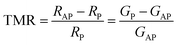 | (8) |
where RP and GP represent the resistance and conductance when the magnetization directions of the two ferromagnetic electrodes are parallel, respectively, and RAP and GAP represent the corresponding values in the antiparallel state.172 Several factors have a substantial effect on the TMR ratio. The first is interface quality. The roughness of the contact between the barrier layer and the ferromagnetic electrode has a substantial impact on tunnelling coherence. Research indicates that reducing the roughness of the SFMO/MgO interface from 1.0 nm to 0.3 nm can boost the room-temperature TMR ratio from 80% to 120%. This is due to the reduced interface scattering and improved tunnelling electron coherence.35 The second is the thickness of the insulating layer. It is necessary to carefully adjust the thickness of the barrier layer (tb) (e.g., MgO) since an extremely thin layer can cause pinholes and leakage current, while an excessively thick layer can result in an overly weak signal because of the exponential decrease of tunnelling probability. High-quality LaMnO3+δ/La0.7Ca0.3MnO3 multilayer structures were constructed in an attempt to establish all-oxide manganite tunnel junctions, and tunnel studies using Au/Ir electrodes and LaMnO3+δ barrier layers were successfully carried out at low temperatures. Even when the junction area was roughly 0.02 mm2 and the barrier thickness reached 20 nm, the tunnel effect was still noticeable.174 The third is the temperature stability. DPOHMs outperform typical half-metal oxides (e.g., Fe3O4) in terms of high-temperature performance, making them ideal for devices in difficult environments.175 Kumar et al. reported the MR effect of MTJs based on SFMO at RT.173
Micron-sized SFMO/STO/SFMO devices were fabricated by the PLD method, as depicted in Fig. 11. The current–voltage curves of the MTJ devices at room temperature exhibit nonlinear and asymmetric behaviour, consistent with the prediction of tunnel conductivity. The large TMR (TMR ≈ 7%) effect observed at room temperature is attributed to the spin-dependent tunnelling effect generated by the uniform ultra-thin STO tunnel barrier layer between the two identical SFMO electrodes (bottom and top) in the MTJ device.
 |
| | Fig. 11 (a) Schematic diagram of an SFMO/STO/SFMO three-layer magnetic tunnel junction device. (b) Cross-sectional view of a typical magnetic tunnel junction device field emission scanning electron microscope image173 (reproduced with permission from The Royal Society of Chemistry, 2014). | |
5.3.2 Magnetoresistance (MR) and spin-dependent scattering.
The MR effect describes the relative change in material resistance under an applied magnetic field, and its microscopic mechanism is strongly related to spin-dependent scattering processes, which primarily include giant magnetoresistance (GMR) and AMR. When a nonmagnetic metal layer separates ferromagnetic/nonmagnetic/ferromagnetic sandwich structures (spin valves), the GMR phenomenon typically takes place. Its fundamental physical property is that the relative relationship between the electrons' spin direction and the ferromagnetic layer's magnetization direction determines their transport resistance. A notable resistance change happens when the two ferromagnetic layers' magnetization directions change from antiparallel (high-resistance state) to parallel (low-resistance state). The spin diffusion length of the nonmagnetic intermediate layer has a major influence on the amplitude of GMR; the longer this length, the more powerful the GMR impact is and the better the spin information is kept throughout transit.176 Using the same preparation circumstances, Naushahi et al. investigated the impact of deposition distance on a set of SFMO thin films grown by PLD. Longer-distance deposited thin films showed improved metallicity and magnetoresistance responsiveness. High-quality SFMO thin films and multilayer structures for upcoming room-temperature spin valve devices are mostly due to the observed Fe–Mo cation stoichiometric imbalance, which modifies magnetic interactions and reshapes magnetoelectric characteristics.177 Abbasi studied MTJs composed of two half-metallic ferromagnetic La2/3Sr1/3MnO3 (LSMO) manganite electrodes and a La2NiMnO6 (LNMO) double perovskite ferromagnetic insulating barrier.178 The resistance of the junction strongly depends not only on the orientation of the magnetic moments in the LSMO electrodes but also on the orientation of the LNMO barrier magnetization relative to the LSMO magnetization. As shown in Fig. 12(a), the tunnel magnetoresistance ratio reaches a maximum of 24% at 10 K and gradually decreases with increasing temperature until it disappears completely above the LNMO critical temperature of 280 K. Magnetic insulating barrier is an interesting approach to achieve room-temperature MR effects in oxide-based heterostructures. In the temperature range of 185–300 K, the junction exhibits semiconductor-like behaviour, with resistance increasing as temperature decreases—consistent with the direct tunnelling transport characteristic in the junction at 300 K, as shown in Fig. 12(b). The GMR value observed in spin valves with a similar structure decreases to about 35% when Cu is utilized as the intermediate layer because of its comparatively significant spin scattering, demonstrating that the intermediate layer material plays a crucial role in spin-polarized transport.179
 |
| | Fig. 12 (a) Temperature dependence of junction resistance in zero magnetic field and 0.2 T magnetic field. The inset shows the difference between the two curves (MR effect), which approaches zero at 275 K. (b) Voltage–conductivity relationship for a multilayer magnetic tunnel junction device. Dark blue squares and dark red circles represent conductivities at 10 K and 300 K, respectively178 (reproduced with permission from The Royal Society of Chemistry, 2024). | |
5.3.3 Spin relaxation time (τs).
One important dynamic parameter that directly affects the effective transport distance of spin information or spin current is the spin relaxation time (τs), which measures how long the spin-polarized state can be sustained in a material. In experiments, the most popular pump–probe method for examining ultrafast spin dynamics and obtaining τs is the time-resolved magneto-optical Kerr effect (TR-MOKE). This method employs a delayed probing light to monitor the magnetization recovery process and a femtosecond laser pulse (pump light) to immediately disturb the magnetization equilibrium; the characteristic time of the magnetization relaxation curve can be used to determine the τs.180,181 Experiments have demonstrated the spin relaxation properties of several DPOHMs. The double perovskite structure of Ba2CaWO6−δ (δ = 0) is B-site ordered, and its octahedral tilt angle varies with temperature. W5+ (d1) spin centers with S = 1/2 and I = 0 can be produced by oxygen vacancies in this structure. The viability of these qubit candidates is confirmed at T = 5 K, τ1 = 310 ms, and τ2 = 4 µs. τ2 has remarkable stability with rising temperature, remaining constant below T = 60 K, decreasing to about 1.0 µs at T = 90 K, and remaining fairly constant until T = 150 K. This suggests that the application range of possible materials in quantum information science can be increased and that suitable paramagnetic point centers for quantum applications can be produced by systematically introducing defects in the double perovskite structure.182
6. Theoretical calculation models of DPOHMs
One essential tool for determining the origin of the electrical structure of DPOHMs, directing the creation of new materials, and improving performance is theoretical computation. The DFT framework serves as the primary foundation for current research, and sophisticated techniques like the GW approximation and Hubbard U correction (DFT+U) are presented to better characterize their highly coupled electrical behaviour. Relevant calculation models, common applications, and theoretical advancements are methodically introduced in this part.
6.1 Basic calculation models: DFT and U correction (DFT+U)
6.1.1 DFT principles and exchange–correlation functionals.
The ground state characteristics of a many-electron system are converted into a problem of non-interacting electrons moving in an effective potential field by DFT using the Hohenberg–Kohn theorem and Kohn–Sham equations. The exchange–correlation functional is its fundamental approximation. The local density approximation (LDA), generalized gradient approximation (GGA), and GGA+U are examples of functionals that are frequently employed. The bandgaps of transition metal oxides are typically underestimated or not predicted at all using LDA, which solely depends on the local electron density and performs well for simple metal systems. In general, GGA predicts atomic structures and lattice constants more accurately than LDA and takes into account the gradient of the electron density. One of the most popular GGA functionals is the PBE functional.183 By adding the Hubbard U parameter on top of GGA, GGA+U is intended to address the Coulomb repulsion of localized d or f electrons and rectify the standard DFT's inability to adequately describe strongly correlated systems (such as transition metal d-electrons). This approach is now the norm for researching DPOHMs' electrical structures.184 The outcomes of the calculation depend heavily on the U parameter selection. The U value is often chosen in the range of 3–5 eV for 3d transition metals with significant electron correlation effects (like Fe, Co, and Ni); it is typically set in the range of 1–3 eV for 4d/5d metals with more extended orbitals and weaker correlation effects (like Mo and Re).185 Using SFMO as an example, GGA+U calculations produce a spin-minority bandgap of around 0.4 eV, which is in good agreement with the experimental value (≈0.38 eV)13 when UFe = 4 eV is applied to the Fe 3d orbitals and UMo = 2 eV is applied to the Mo 4d orbitals. Strong correlation effects must be taken into account because, in contrast, employing normal GGA (U = 0) produces a metallic state and is unable to replicate its half-metallic feature.53,186
6.1.2 Structural optimization and band structure calculation.
Structural optimization is the first and most important stage in theoretical investigations of double perovskite oxides. It aims to achieve a stable ground-state geometric structure by iteratively altering atomic locations and lattice constants in order to reduce the system's total energy. There is a high degree of consistency between theoretical calculations and experimental measurements in examples of structural optimization. Following structural optimization using the GGA+U method, the lattice constant for SFMO is approximately 3.91 Å (for the simple cubic cell) or ≈7.82 Å (for the primitive cell). This represents a minimal deviation (<0.3%) from the experimental XRD values of approximately 3.905 Å13 or approximately 7.822 Å,53,186 indicating the computational model's dependability. The direct theoretical foundation for determining whether a material is half-metallic is band structure computation. One spin channel (typically spin-up) in the spin-resolved band structure has electronic states at the Fermi level (EF) that exhibit metallic behaviour, while the other spin channel (spin-down) has a finite bandgap at EF that exhibits insulating behaviour. This is the typical feature of half-metallicity. The regulatory patterns of half-metallicity are revealed by the capacity to carry computational instances. The substitution of Os atoms for Fe in double perovskite structure oxides can result in a half-metallic antiferromagnet: the conduction band electrons crossing the Fermi level have 100% spin polarization but show no net magnetization, according to electronic structure calculations based on DFT (using the GGA) for the double perovskites SFMO and Sr2OsMoO6. The HM antiferromagnetic state is still present, according to GGA+U electronic structure calculations.187 In line with earlier findings based on model calculations, kinetic energy-driven stabilization of the antiferromagnetic phase occurs in La-enriched compounds, as demonstrated by first-principles density functional calculations in conjunction with exact diagonalization of a Fe–Mo Hamiltonian built from first-principles Wannier functions.10 Recently, the band structures and density of states of Ca2TiFeO6 HM DP oxides were also calculated by DFT by employing the projector augmented wavelet (PAW) method with a plane wave basis.188 The GGA, as proposed by Perdew–Burke–Ernzerhof (PBE),183 was used to evaluate the exchange and correlation energies. A Hubbard U correction (GGA+U) was applied to better account for the strong on-site Coulomb interactions, where the Hubbard U potential values were selected as UTi = 2.5 eV and UFe = 5.3 eV. The Hubbard U corrections in DFT calculations are very important to accurately describe the electronic and magnetic properties of transition metals, especially in materials with strong electron–electron interactions. Fig. 13(a) and (b) shows the calculated band structure of the Ca2TiFeO6 HM DP compound with the spin-up (left) and spin-down (right) orientations, respectively.189 This spin-polarized band analysis provides crucial insights into the material's conduction properties and magnetic behaviour. As shown in Fig. 13(a), in the ground state the material displays a metallic feature for the up-spin orientation, as multiple bands cross the Fermi level. In contrast, for the down-spin polarization (Fig. 13(b)), a semiconducting behaviour with a direct bandgap of 2.3 eV is observed. This combination of characteristics confirms the half-metallic semiconducting nature of the Ca2TiFeO6 compound. The discrepancy between the theoretical and experimental bandgap values is ascribed to the fact that DFT calculates the energy difference between the valence and conduction bands, but the bandgap obtained via diffuse reflectance spectroscopy corresponds to the photon absorption threshold, which indicates the energy required to generate an exciton, a bound state of an electron and a hole created by the electrostatic Coulomb interaction upon photon absorption.
 |
| | Fig. 13 Calculated electronic band structure for the Ca2TiFeO6 compound, with the contributions from (a) spin-up (left) and (b) spin-down (right) orientations. (c) Total DOS for Ca2TiFeO6 contributed by spin-up orientation (black curve) and spin-down orientation (red curve), respectively. (d)–(f) Partial DOS (PDOS) in Ca2TiFeO6 contributed by Ti-d, Fe-d, and O-p orbitals for the spin-up and spin-down configurations, respectively189 (reproduced with permission from Elsevier Ltd, 2025). Total DOS for Ca2TiRuO6 calculated by GGA-PBE (g) and GGA+U-PBE (h) close to the Fermi level with the inclusion of spin–orbit coupling (SOC)26 (reproduced with permission from The Royal Society of Chemistry, 2025). | |
6.2 Density of states (DOS) and magnetic moment analysis
A crucial theoretical tool for comprehending the origin of half-metallicity and magnetism in materials is the DOS, which characterizes the distribution of electronic states in energy space. It is possible to clearly see the electrical behaviour of several spin channels and the contribution of each atomic orbital by examining the total density of states and partial density of states (PDOS).
6.2.1 Total DOS and partial DOS (PDOS).
A material's HM properties are directly reflected in its total DOS. For an ideal half-metal, the total DOS exhibits notable spin asymmetry at the Fermi level (EF): one spin channel, such as spin-up, has a finite DOS at EF, displaying metallic behaviour, while the other spin channel, spin-down, has zero DOS at EF, with a distinct bandgap. For instance, calculations for SFMO reveal that the spin-down channel has a bandgap of approximately 0.4 eV at EF, theoretically predicting its 100% spin polarization ratio.13,53 The microscopic orbital genesis of half-metallicity is further shown by partial density of states (PDOS) investigation. The hybridization between the d-orbitals of the transition metal ions at the B- and B′-sites and the p-orbitals of the oxygen anions is the main cause of half-metallicity in DPOHMs. Using SFMO as an example, its PDOS analysis shows that both Fe 3d (particularly eg orbitals) and Mo 4d (t2g orbitals) contribute significantly at the Fermi level, making them the primary carriers for conduction in the spin-up channel. Concurrently, O 2p orbitals exhibit substantial hybridization with these d-orbitals; their DOS accounts for around 30% in the vicinity of EF, indicating the critical role that p–d hybridization plays in the formation of the conduction channel. The bandgap opens in the spin-down channel when the DOS of the Mo 4d and Fe 3d orbitals falls to zero close to EF. Strong electron correlation and p–d hybridization caused by a particular crystal field environment work together to form this energy gap.13,190
In order to examine the specific contributions of the electronic orbitals near the Fermi level, the DOS of Ca2TiFeO6 was calculated for the spin-up and spin-down configurations, as shown in Fig. 13(c)–(f).189Fig. 13(c) presents the total DOS contributed by spin-up polarization (black curve) and spin-down polarization (red curve), respectively. It is noticed that near the Fermi energy (EF = 0 eV) there is a significant difference between the DOS for both spin configurations. As observed in the calculated band structure, the up-spin configuration (Fig. 13(a)) exhibits states crossing the Fermi level, indicating metallic behaviour, whereas the down-spin configuration shows a semiconducting gap. Thus, the total DOS presented in Fig. 13(c) agrees with the band structure, clearly demonstrating the above-mentioned HM behaviour. To enhance the visibility of key electronic states near EF, zoomed-in insets are added to highlight the subtle features close to the Fermi level. The PDOS contributed by Ti d-orbitals and Fe d-orbitals for the spin-up and spin-down configurations is shown in Fig. 13(d) and (e), respectively. As shown in Fig. 13(d), the Ti d-orbitals in the spin-up configuration contribute minimally close to EF, which means these electronic states make a few contributions to the observed metallic conduction for this spin configuration. To better illustrate the Ti-d states’ weak contributions near the conduction band edge, an additional zoomed-in inset is incorporated. For the spin-down configuration, the Ti d-orbitals positioned below the Fermi energy make no direct contributions to the conduction states, thus contributing to the non-conducting nature of this spin polarization. In Fig. 13(e), the Fe d-orbitals in the spin-up configuration show a significant contribution near the Fermi level, accounting for the metallic behaviour in this configuration. However, in the spin-down configuration, the Fe d-orbitals display a clear separation between the occupied states in the valence band and unoccupied states in the conduction band, leading to the formation of a bandgap. The asymmetry between the contributions from spin-up and spin-down polarizations highlights the strong spin polarization, where the Fe d-orbitals are the primary contributors to the magnetic moment of the compound. The PDOS contributed by O p-orbitals in the spin-up and spin-down configurations is shown in Fig. 13(f). It is observed that the O p-orbitals make significant contributions to the DOS near the Fermi level. For the up-spin configuration, the O p-orbitals occupy states between −4.8 eV and 0.3 eV, suggesting the hybridization with the d-orbitals of Ti and Fe. This result underscores the importance of Fe–O–Ti inter-octahedral bonds in the conductive and ferromagnetic behaviours of the compound. In contrast, for the down-spin configuration, the O p-orbitals are mainly located in the valence band, between −4.6 eV and −0.3 eV, contributing to the semiconducting character of this compound. The interactions between the O p-orbitals and the d-orbitals of Ti and Fe indicate the occurrence of hybridizations that influence both the electrical charge transport properties and the magnetic ordering of the compound. The above analysis confirms that Fe is the dominant source of magnetization in the system, while Ti and O contribute marginally to the overall ferromagnetic response. The strong Fe–O–Ti hybridization observed in the DOS analysis further reinforces the role of orbital interactions in shaping the magnetic and electronic behaviour of the compound.
To assess the effect of the SOC on the electronic states of Ca2TiRuO6 HP oxides in the vicinity of the Fermi level, GGA-PBE (Perdew–Burke–Ernzerhof) and GGA+U-PBE calculations were carried out, and the results are shown in Fig. 13(g)–(h).26 It is important to note that the incorporation of SOC in the DFT calculations for the study of the electronic properties of the Ca2TiRuO6 material eliminates the distinction between the spin channels, due to the inclusion of the SOC producing a mixture of electronic states that are described by combinations of the orbital quantum numbers (l, m), eliminating the explicit spin separation. Based on the DFT calculations it is found that strong SOC effects are associated with the half-metallic feature, which play an important role in the emergence of half-metallicity in perovskite materials, particularly in double perovskites with transition elements occupying at B-sites. Thus, the strong SOC effect may have given rise to the half-metallic nature exhibited by double perovskites containing transition elements.
6.2.2 Magnetic moment calculation and SE interaction.
The unpaired d-electrons of the transition metal cations at the B- and B′-sites are the primary source of the net magnetic moment of DPOHMs. By integrating the electron population of spin-up and spin-down channels, the theoretical total magnetic moment can be directly determined by first-principles computations. The B-site ion in SFMO is usually thought of as high-spin Fe3+ (3d5, S = 5/2), with a theoretical spin magnetic moment of roughly 5.0μB, and the B′-site Mo ion is usually thought of as Mo5+ (4d1). Through oxygen-mediated SE, its magnetic moment interacts ferromagnetically with Fe3+, producing a little magnetic moment at the Mo site (about −1μB) that opposes but does not completely cancel the Fe site moment. With slight differences that could be caused by cation disorder or measurement errors, the theoretically anticipated saturation moment is around 4.0μB f. u.−1, which is in basic agreement with the experimentally determined saturation magnetization of ∼3.8μB f. u.−113 or ∼3.4μB f. u.−1.191 The theoretical total magnetic moment for LCMO is predicted to be 6.0μB f. u.−1, assuming that there is ferromagnetic coupling between Co2+ (3d7, S = 3/2) and Mn4+ (3d3, S = 3/2). The material's anti-site defects (Co/Mn disorder) cause antiferromagnetic coupling, which partially cancels the net moment. This is the main reason why the experimentally measured saturation moment is typically lower than this value (e.g., ∼5.8μB f. u.−1![[thin space (1/6-em)]](https://www.rsc.org/images/entities/char_2009.gif) 192). The magnetic exchange coupling constant (J), where J > 0 denotes ferromagnetic coupling and J < 0 shows antiferromagnetic coupling, can be used to quantitatively assess the strength and sign of the SE interaction. Calculations for SFMO demonstrate that the ferromagnetic exchange constant J for the Fe–O–Mo channel is roughly 20 meV, confirming its medium-strength ferromagnetic coupling as the basis for the high Curie temperature.193 Furthermore, the impact of imperfections on magnetism is also investigated by theoretical simulations. For instance, Wu et al. investigated the impact of oxygen vacancies on the half-metallic characteristics of the perovskite oxide SFMO using density functional calculations.194 The compound showed half-metallic properties over the range of oxygen vacancies, and as the amount of oxygen vacancies increased, the spin-up channel bandgap shrank. Fe and Mo ions were found in high-spin and intermediate-spin states, respectively, in all compounds. The magnetic moment of Mo ions increased while that of Fe ions decreased as the oxygen vacancy content increased. This suggests that over a broad range of δ values, Sr2FeMoO6−δ exhibits half-metallic properties, providing a viable avenue for the experimental production of useful half-metals with trace quantities of oxygen vacancies.
192). The magnetic exchange coupling constant (J), where J > 0 denotes ferromagnetic coupling and J < 0 shows antiferromagnetic coupling, can be used to quantitatively assess the strength and sign of the SE interaction. Calculations for SFMO demonstrate that the ferromagnetic exchange constant J for the Fe–O–Mo channel is roughly 20 meV, confirming its medium-strength ferromagnetic coupling as the basis for the high Curie temperature.193 Furthermore, the impact of imperfections on magnetism is also investigated by theoretical simulations. For instance, Wu et al. investigated the impact of oxygen vacancies on the half-metallic characteristics of the perovskite oxide SFMO using density functional calculations.194 The compound showed half-metallic properties over the range of oxygen vacancies, and as the amount of oxygen vacancies increased, the spin-up channel bandgap shrank. Fe and Mo ions were found in high-spin and intermediate-spin states, respectively, in all compounds. The magnetic moment of Mo ions increased while that of Fe ions decreased as the oxygen vacancy content increased. This suggests that over a broad range of δ values, Sr2FeMoO6−δ exhibits half-metallic properties, providing a viable avenue for the experimental production of useful half-metals with trace quantities of oxygen vacancies.
6.3 Theoretical simulation of defect effects
Defects are important determinants of the electrical structure, magnetism, and transport characteristics of DPOHMs, particularly oxygen vacancies, cation doping, and ASDs. The formation energy of defects can be quantitatively assessed using first-principles calculations, which also provide a detailed understanding of the microscopic mechanism by which defects control material properties.
6.3.1 Oxygen vacancies.
 are one of the most prevalent point defects in DPOHMs. Their formation energy (Ef) is a key parameter for assessing their stability in a specific environment, typically calculated using the formula:
| |  | (9) |
where Etot is the total energy, E(O2) is the O2 molecule energy,195 and μO is the oxygen chemical potential, whose value depends on the specific synthesis atmosphere (e.g., oxidizing or reducing conditions).196 Under reducing circumstances, the  formation energy of SFMO is around 2.5 eV. According to theoretical estimates, adding
  reduces the gap width from 0.4 eV to roughly 0.2 eV, which lowers the material's spin polarization ratio by generating impurity energy levels within the bandgap of the initially insulating spin-down channel.16,197 This explains the experimentally observed deterioration of magneto-transport performance caused by
  from the standpoint of electronic structure. Comprehensive first-principles computations on LCMO and its variation with Co–Mn–Mn–Co ASDs were carried out by Yuan et al.198 They discovered that both Co and Mn prefer to show a +3 state at anti-sites, while their covalent states are +2 and +4 at regular sites, respectively. The
  formation energy was projected to obey the following trend: Co2+–O–Mn4+ > Co2+–O–Co3+ > Mn3+–O–Mn4+. Stronger electron delocalization between mixed-covalent transition metals (Co2+–O–Co3+ and Mn3+–O–Mn4+) was identified as the microscopic mechanism; this effect efficiently reduces electron repulsion and promotes vacancy stability. Through calculations, Antonov et al. were able to determine how
  alter the valence states of transition metal ions, hence influencing characteristics. They observed that the potential
  led to mixed valence states at the Cr sites, generating a double-peak structure at the Cr L2,3 edges in SCWO and SCRO and lowering the saturation magnetization.199 This suggests that more energy is needed to form
  in this material, meaning that it is more resistant to them. This suggests that the material can sustain structural stability and consistent performance in high-temperature application settings.
6.3.2 Element doping.
The stability of doping elements and their regulating effects on material properties can be accurately predicted by first-principles calculations, which also offer theoretical directions for experimental design. The computed doping formation energy is negative (about −0.5 eV) when A-site doping is carried out with La3+ in place of Sr2+ in SFMO, suggesting that the doping process is thermodynamically advantageous. By raising the electron occupation of Mo 4d orbitals close to the Fermi level and strengthening the hybridization between Mo 4d and O 2p orbitals, electronic structure analysis demonstrates that the addition of La3+ is similar to injecting electrons into the system. The material's half-metallicity and spin polarization ratio are improved by this enhanced p–d hybridization, which promotes widening of the bandgap in the spin-down channel.200,201 Properties can also be efficiently tuned by element replacement at the B-site. For instance, the electronic structure and magnetic characteristics of the pseudo-cubic and tetragonal double perovskite oxides Sr2MnNbO6(SMNO), SFMO, and Sr2NiRuO6 (SNRO) were ascertained utilizing the full-potential linearized augmented plane wave (FP-LAPW) approach inside the local spin density approximation (LSDA)+U scheme. The crystal structures of all three compounds showed half-metallic properties. The third compound favoured the pseudo-cubic shape, whereas the previous two tended to form tetragonal structures. SFMO showed antiferromagnetic order, but SMNO and SNRO were ferromagnetic. The spin–orbit coupling effect varied with the 3d and 4d orbital magnetic moment values in the elemental sequence from Nb to Ru and from Mn to Ni, exhibiting an increasing trend from quenched to weakly unquenched to unquenched. In accordance with the e2g–0–e0g Goodenough–Kanamori–Anderson (GKA) model for SE, SNRO demonstrated half-metallic conductivity and ferromagnetism.202 The predictive power of theoretical computations is what gives them their potency. For instance, the electronic structure and magnetic properties of the double perovskite compounds SFMO, SFRO, and SCWO were investigated using the full-potential linear muffin-tin orbital method within the LSDA and GGA frameworks. HM ferromagnetic band structures were anticipated by the calculations to have total spin magnetic moments of 4.0μB for SFMO, 3.0μB for SFRO, and 2.0μB for SCWO. These investigations offer a precise theoretical foundation and guidance for investigating and creating novel double perovskite oxides with enhanced characteristics.203
6.4. Limits of current theoretical models and their perspectives
The sensitivity of half-metallicity prediction to the U value, exchange correlation functional, and SOC is indeed high, especially for the 5d systems (such as Re-based DPOHMs). The choice of U value directly affects the band structure: a too small U value may lead to mis-judgment of metallicity, while increasing the U value appropriately can drive the system to achieve half-metallic properties. The 5d system requires careful selection of U values because the 5d electron correlation is weak (U ∼ 1.0 eV), but the SOC is strong. If the U value is too high, it will cause band splitting and damage the half-metallic properties. It is suggested that optimization of the U value can be achieved through Bayesian calibration or the experimental data. GGA may underestimate the bandgap, resulting in mis-judgment of half-metallicity. Thus, introducing the Hubbard U term in GGA+U can correct for strong correlation effects, but attention should be paid to the empirical value of U. For the 5d systems, meta-GGA functionals (such as strongly constrained and appropriately normed, SCAN) can more accurately describe electronic correlations, but the computational cost is relatively high. Considering the strong SOC effect in the 5d system, it can cause band splitting and affect the HM properties. For example, in the Re-based HM perovskites, SOC may disrupt spin degeneracy and need to be explicitly included in the calculation. In addition, the SOC effect may vary with temperature and need to be predicted in conjunction with finite temperature transport models such as Ham GNN. Special consideration should be given to the 5d system, which needs to balance electronic correlation (U) and SOC (λ), and it is recommended to optimize these parameters through phase diagram analysis (such as the U–t–λ triangle). On the other hand, theoretical predictions can be verified by the experimental data (such as angle-resolved photoelectron spectroscopy (ARPES) or transport experiments).
The current theoretical models can provide reliable guidance in material design, but some limitations such as data scarcity, complex calculations, and dynamic effects still need to be addressed. It is suggested that combining experimental verification and multi-scale calculations can improve the design reliability. For example, through first principles calculations and machine learning, the model can predict material properties (e.g., catalytic activity and electronic structure) and guide experimental synthesis. In addition, model predictions also need to be validated through experiments (e.g., the design of calcium single atom materials supported by graphene doped with heterogeneous atoms, which have been verified for their hydrogen storage capacity through practical testing). However, the current model accuracy is limited by the quality and quantity of training data due to the high-quality datasets being scarce in materials science. High precision calculations (such as DFT+U) are costly and limit the application of complex systems.
7 Applications and challenges of DPOHMs in magnetic storage
7.1 Core application scenarios
7.1.1 MTJs and magnetic random access memory (MRAM).
With the high spin polarization ratios and adjustable magnetic anisotropy, DPOHMs are thought to be the perfect electrode materials for the next-generation MTJs, which should greatly increase the TMR effect and lower device power consumption. The room-temperature TMR ratios of current mainstream MTJs based on CoFeB/MgO/CoFeB structures are often between 100% and 200%, and the write current density needed for magnetization switching is typically greater than 106 A cm−2204,205 (Fig. 14). The following performance benefits are provided by DPOHM-MTJs. LSMO/BaTiO3/LSMO heterostructures and other all-perovskite MTJs have demonstrated exceptional overall performance (Fig. 15). In contrast to traditional TMR, three magnetic field-induced resistance states were eventually formed by the observation of four separate zones with elevated MR. It is possible to mimic the low-field MR effect using a model that is based on structural flaws and non-uniform strain in the LSMO layer, which are caused by the significant lattice mismatch between the LSMO and the MgO substrate. This discovery facilitates the comprehension of intricate MR effects in multilayer MTJs and can serve as a guide for the development of brain-like devices or multi-bit memory cells.206,207 Another important factor in hybrid structure MTJs is performance. An MTJ using La0.3Sr1.7FeMoO6 as one electrode and conventional CoFeB as the other, for example, demonstrated excellent application potential with a room-temperature TMR of roughly 200% and an expected data retention period well over 10 years.173,179 Leaders in the industry, such as Samsung Electronics, have kept a careful eye on the potential applications of these materials. According to research reports, MRAM technology prototypes based on DPOHMs such as SFMO have the potential to improve key indicators like storage density by several times when compared to traditional solutions. This represents a significant trend in which these materials are progressing from basic research to application exploration.208 Asano et al. first reported the TMR performance of micron-sized SFMO-MTJ junctions fabricated by a standard photolithographic process.209 The SFMO junctions with a native barrier formed by surface oxidation of a SFMO based-electrode and a Co counter electrode exhibited a TMR value of 10% at 4.2 K. Recently, Kumar et al. also reported the TMR performance of micrometre-sized SFMO-MTJ (SFMO/STO/SFMO) devices fabricated by the PLD method.210 The thickness of the bottom and top electrodes of SFMO was ∼150 nm and ∼50 nm, respectively, and the thickness of the STO barrier layer was kept about 2 nm. A metal shadow mask with lateral dimensions of 40 µm × 40 µm were used to fabricate the SFMO/STO/SFMO MTJ devices. At room temperature, the MTJ devices exhibited a TMR ratio of 7% at 300 K, which was ascribed to the spin-dependent tunnelling across a uniform ultrathin STO tunnel barrier in the micron-sized MTJ devices. From the TMR ratio of the micron-sized MTJ device, the SP of the SFMO layers in MTJ devices was deduced to be ∼18% at 300 K by using classical Julliere expression.172 Nanometer-sized SFMO/STO/Co MTJ devices were obtained by combining a three-step process for the growth of the SFMO layer by PLD. Transport measurements revealed a clear MR behavior with a positive TMR of about 50% at 4 K. This TMR ratio corresponds to a very large negative SP value (SP = −85%) and confirms the half-metallic character of SFMO and its potential for fully spin-polarized tunnelling.211
 |
| | Fig. 14 (a) Schematic cross-section of the fabricated magnetic tunnel junction.171 The MgO thickness is fixed at 0.85 nm. (b) Scanning electron microscopy image of the etched pillars, showing the fabricated pillar area of 80 × 240 nm2 (reproduced with permission from The Royal Society of Chemistry, 2024). | |
 |
| | Fig. 15 Schematic diagram of the patterned sample structure207 (reproduced with permission from The Royal Society of Chemistry, 2005). | |
7.1.2 Spin valves and magnetic sensors.
DPOHM-based spin valve structures can be used to create extremely sensitive magnetic sensors by taking advantage of their strong giant magnetoresistance (GMR) effect. These sensors offer a wide range of potential uses in non-contact sensing, biological imaging, and magnetic field detection. Spin valves based on DPOHM operate exceptionally well. According to research reports, DPOHM materials such as LCMO can be used to build magnetic sensor prototypes that can detect weak magnetic fields as low as 10−5 Oe.212,213 These high-sensitivity sensors open up new technological avenues for the detection of weak magnetic field signals and precise placement, and associated research and development activities are constantly advancing them toward real-world use.
7.1.3 Spin metal-oxide-semiconductor field-effect transistors (spin-MOSFETs).
In order to provide effective spin injection and manipulation and offer solutions for low-power, high-performance logic devices, DPOHMs can be used as spin injection electrodes in spin field-effect transistors (spin-MOSFETs) due to their high spin polarization ratio. Sugahara and Tanaka methodically presented the idea for this device, which revolved around the usage of half-metallic ferromagnets as source/drain electrodes. According to theoretical research, spin-MOSFETs made of these materials (for example, with SFMO as the electrode) should be able to drive current at a rate of roughly 0.5 mA µm−1 and produce a high on/off current ratio (Ion/Ioff) of up to 106.214 The model device utilized in this investigation, which uses a thin-film transistor topology for easier computation, is demonstrated in Fig. 16(a). The channel length, Lch, of the model device is 30 nm, the silicon layer thickness is 10 nm, and the gate oxide (SiO2) thickness tox is 2.0–3.0 nm. The distance between the source/drain junction and the non-magnetic contact is represented by the device parameters LS (LD) in Fig. 16. It is expected that spin-polarized electrons injected into the channel follow ballistic transport, and the channel uses an inherent silicon layer. This theoretical forecast shows how spin-MOSFETs have a lot of potential to replace conventional transistors in logic operations. Related research studies have continued to advance in recent years. For instance, spin-MOSFETs using LCMO as source/drain electrodes were investigated in theoretical design and performance simulation studies. Based on the simulation studies, such devices should have an intrinsic delay time of less than 10 ps and a switching ratio of 105 at room temperature.215 These features imply that DPOHM-based spin devices might be able to satisfy the application requirements of upcoming low-power, high-frequency integrated circuits. Effective spin transmission and long-distance maintenance in the channel are two major scientific obstacles that this subject still faces, and related research is still in the exploratory stage. A comparison of the performance metrics of the above magnetic devices based on different DPOHMs is presented in Table S3.216–219
 |
| | Fig. 16 (a) Device structures and (b) and (c) band diagrams of spin MOSFETs with magnetization directions (b) (parallel) and (c) (anti-parallel). Solid arrows in the HMF source/drain indicate up-spin and down-spin electrons at the Fermi level of the metallic spin band and the valence band edge of the insulating spin band, respectively. Dashed arrows represent the conduction band edge of the insulating spin band in the HMF source/drain214 (reproduced with permission from The Royal Society of Chemistry, 2004). | |
7.2 Key technical challenges
7.2.1 Difficulty in regulating the crystal ordering degree.
The primary structural factor influencing the half-metallicity of double perovskite oxides is the ordering degree (S) of the B-site and B′-site transition metal ions. However, the following factors make it extremely difficult to achieve near-perfect cation ordering (S > 0.95) on a macroscopic scale, particularly in large-area thin films. First, the precision of the synthesis process is limited. SFMO films prepared by using traditional physical deposition techniques (such as magnetron sputtering and pulsed laser deposition) usually have an ordering degree of 0.85 to 0.92. Extremely exact coordinated control of the substrate temperature, post-annealing process (temperature variation must be kept under ±5 °C), and oxygen partial pressure is necessary to raise the ordering degree to over 0.95.71,220,221 Anti-site flaws can develop from even the smallest variation, greatly impairing the material's inherent performance. The second is the challenge of managing extremely volatile substances. Elements like Mo and Re have high vapor pressures during high-temperature synthesis (for example, Mo's vapor pressure at 1000 °C is about 10−4 Pa). This makes them vulnerable to volatilization from the lattice, which results in deviations in the B/B′ stoichiometric ratio and the introduction of a large number of cation vacancies, both of which significantly impede the formation of long-range ordered structures.150,222,223 Researchers have searched for a number of solutions to solve these issues. The film ordering degree can be raised to 0.98 by employing methods such as co-sputtering from dual targets, which accurately control element transport and stoichiometry at the source by independently and simultaneously adjusting the sputtering power of B-site and B'-site metal targets.71,220 Starting with precursors made using the citrate procedure, a high-pressure method was used to successfully synthesize the polycrystalline DP SFMO material with substantial anti-site disorder. Because the ordered sample had a smaller lattice volume, applying high pressure (2 GPa) to SFMO enabled long-range Fe/Mo cation ordering.45 Lattice stability can be improved by adding the right quantity of stabilizing elements (such as Ti4+ and Zr4+) to partially replace volatile B′-site ions and create solid solutions.224
7.2.2 Interface lattice mismatch and scattering.
Device performance is largely dependent on the interface quality with widely used barrier layers (e.g., MgO and Al2O3) when building heterojunctions (e.g., MTJs based on DPOHMs). The two primary issues at the moment are element interdiffusion and lattice mismatch. DPOHMs and barrier layers or insulating substrates differ significantly in their lattice constants. For instance, SFMO has a lattice constant of roughly 3.93 Å, but MgO has a lattice constant of 4.21 Å. This leads to a mismatch rate of up to 7.1%. The coherence of tunnelling is destroyed by this mismatch, which results in a high density of misfit dislocations at the interface (up to 1010 cm−2), acting as strong electron scattering centers and drastically lowering the TMR ratio by 20% or more.86,225,226 Element interdiffusion at the interface occurs during the high-temperature annealing necessary for gadget manufacture. For instance, non-magnetic magnesium-iron oxides (such as MgFeO4) and other secondary phases may develop in the interfacial area when magnesium atoms penetrate 1–2 nm from the MgO barrier layer into the DPOHM electrode layer. The magneto-transport performance of the device is hampered by these non-magnetic phases, which drastically lower the effective spin polarization at the interface.11,25 Numerous strategies have been developed by researchers to maximize interface quality. Placing a strain buffer layer between the DPOHM and the barrier layer, an ultrathin metal buffer layer (such as 0.5 nm of Cr) can be inserted to gradually adjust the lattice constant. This lowers the mismatch rate from approximately 7% to less than 3%, which suppresses dislocation formation and enhances TMR performance.227 By using the atomic layer deposition (ALD) technique to create the MgO barrier layer, atomically flat interfaces can be achieved, allowing interface roughness to be controlled to 0.3 nm. The coherence of tunnelling electrons is preserved by such atomically sharp surfaces.204 Interface oxidation passivation: a dense and incredibly thin native oxide layer (approximately 0.2 nm) can be formed by mildly treating the DPOHM film surface with oxygen plasma prior to the barrier layer being deposited. By successfully preventing additional diffusion of elements such as magnesium in later operations, this passivation layer can preserve the inherent qualities of the electrode material.228
7.2.3 High-temperature performance degradation.
When operated in high-temperature environments (usually >400 K), DPOHMs encounter significant structural and performance stability issues, which are mostly expressed as elemental segregation and oxygen vacancy evolution. Elemental segregation happens when the thermodynamic movement of elements is accelerated at high temperatures. For instance, by adding metallic Fe at grain boundaries, a series of Sr2Fe1+xMoO6 (x = 0, 0.03, 0.05, 0.08) ceramic materials were created. Grain boundary (GB) strength was greatly decreased and Fe/Mo ASDs were changed by increasing Fe enrichment. Grain boundaries exhibited a favourable influence on the low-field magnetoresistance (LFMR) effect, but Fe/Mo ASDs had a negative effect.229–231 The term “ evolution” describes the increased mobility of
  at high temperatures (their migration energy barrier is approximately 0.8 eV). The compound displayed half-metallic characteristics across the range of
  , according to DFT calculations on the impact of
  on the half-metallic properties of the perovskite oxide SFMO. Additionally, the spin-up channel bandgap decreased as the
  content increased. Fe and Mo ions were found in high-spin and intermediate-spin states, respectively, in all compounds. The magnetic moment of Mo ions increased and that of Fe ions decreased when the
  content increased.194,232 Rapid thermal processing, A-site chemical doping, and surface coating/core–shell architectures are remedies for the degradation of high-temperature performance. Core–shell structures with Ni–Fe cores and perovskite oxide shells were created by covering DPOHM nanoparticles or films with a thick, inert thin layer. During the reverse water-gas shift chemical looping process, the resultant materials demonstrated higher stability and better performance.233,234 The material's dwell time in the high-temperature zone can be significantly reduced by using millisecond or second-scale rapid thermal annealing or pulsed laser annealing in place of conventional long-time annealing. This effectively suppresses elemental segregation and phase separation, bringing the segregation rate below 2%.235,236 Lattice binding energy and overall structural stability can be improved by doping at the A-site with large-radius rare earth ions such as La3+ and Nd3+. However, the magnetoresistance effect of SFMO is weakened as a result of La/Ba doping at the A-site.233,237
7.2.4 Preparation of large-area high-quality thin films.
Achieving high-quality, extremely uniform thin film manufacturing on 4-inch to 12-inch wafers is necessary to realize the industrial applications of DPOHMs in spintronic devices. The following issues are the primary obstacles in this field. (i) Control of film uniformity: it is difficult for current deposition processes to guarantee consistency in crystal structure, chemical content, and film thickness over wide regions at the same time. For instance, the degree of ordering between Fe and Mo in SFMO films prepared by PLD is dependent on the temperature and pressure during deposition; the highest ordering parameter can approach 85%. As the degree of Fe/Mo ordering increases, saturation magnetization rises to a maximum of 2.4μB f. u.−1. Higher Fe/Mo ordering is much required to obtain greater saturation magnetization.87,238 (ii) Efficiency and cost of preparation: despite PLD readily promoting high-quality epitaxial growth, its limited deposition area and high equipment cost make it unsuitable for large-scale production. When it comes to multi-component oxides like DPOHMs, magnetron sputtering, which is better suited for mass production, generally has poor deposition rates (usually <2 nm min−1), resulting in low production efficiency and high manufacturing costs.239,240
7.3 Future research directions
7.3.1 Multi-element co-doping and exploration of new DPOHMs.
Designing and creating new systems with enhanced performance using a variety of element regulation techniques will be the main focus of future material innovation. Synthesis guided by theoretical predictions: predicting new materials will continue to rely greatly on sophisticated computational techniques like DFT+U and the more precise GW approximation. Potential systems such as Sr2FeRe1−xOsxO6 can be screened using high-throughput calculations; theoretical predictions indicate that these systems may have near-perfect spin polarization ratios and higher Curie temperatures (e.g., >600 K), which would guide the experimental synthesis.203,241–243 Multi-element doping engineering: in addition to single-element doping, multi-element co-doping at the A-site or B-site is anticipated to work in concert to control the materials' magnetic interaction, lattice stress, and electronic structure. For instance, investigating (La and Ba) multi-element co-doped SFMO seeks to further enhance MAE and raise the TC (e.g., to 550 K).244,245 Extension into low-dimensional materials: one new area of study is the extension of DPOHMs from three-dimensional bulk to the two-dimensional limit. For the development of ultra-compact spintronic devices, it is important to synthesize nanosheets (thickness ∼5 nm) of materials such as LCMO using mechanical exfoliation or layered precursor methods and investigate their distinct spin dynamics under dimensional confinement (e.g., possibly longer spin relaxation times).246,247
7.3.2 Heterostructure construction and quantum effect exploration.
Other crucial routes to enhancing device performance and uncovering novel physical characteristics are the construction of new heterojunctions and the investigation of quantum phenomena within them. Using topological insulators in combination: the special spin-momentum locking properties of topological surface states can be used to efficiently increase the interface spin injection efficiency by coupling DPOHMs with topological insulators like Bi2Se3 to create SFMO/Bi2Se3 heterojunctions. This could greatly increase the TMR effect.248 Investigating heterojunctions that occur between DPOHMs and high-temperature superconductors such as YBa2Cu3O7 is known as coupling with superconductors. Such structures may exhibit Josephson or proximity phenomena, which are crucial platforms for basic physics studies and could serve as the basis for future innovations such as spin-superconducting qubits.249 Investigation of quantum transport phenomena: new quantum transport phenomena resulting from band topology features, like quantum tunnelling magnetoresistance, are anticipated to be observed at low temperatures or even at room temperature in heterojunctions made of DPOHMs and topological materials like Weyl semimetals as a result of developments in material growth and interface control technology. This represents a frontier in device physics.250,251
8 Summary and outlook
With high Curie temperature, a nearly 100% spin polarization rate, tunable crystal structures, and superior chemical stability, DPOHMs have emerged as key components for resolving the conflict between “high density, low power consumption, and fast response” in conventional magnetic storage devices. The research advances of DPOHMs are comprehensively reviewed in this work. In terms of structure and synthesis, the rock-salt ordered structure is the cornerstone of half-metallicity; technologies such as PLD and magnetron sputtering can generate high-quality thin films, and the regulation of the ordering degree has exceeded 0.98. Atomic-level structure observation is made possible in microstructural characterization by methods such as synchrotron XRD and AC-TEM, which enable accurate investigation of structural defects such as oxygen vacancies and lattice mismatches. Physical property characterization techniques such as ARS and TR-MOKE have demonstrated that DPOHMs have a lengthy spin relaxation time (>50 ps) and a high spin polarization ratio (>95%). Band structure and defect effects can be precisely predicted by theoretical computing using DFT+U, GW approximation, and multi-scale simulation; AI-assisted design speeds up the screening of new materials even more. With a write current density of only 5 × 10⁵ A cm−2 and a TMR of over 200% in device applications, DPOHM-based MTJs have created new opportunities for improving MRAM performance.
Recently, much progress has been achieved in the synthesis, physical properties and structural characterization of DPOHMs. Some magnetic devices fabricated using DPOHMs have demonstrated their promising applications in digital storage devices and magnetic sensors by making full use of their great GMR effect and HM nature. However, for their industrial applications in magnetoresistive and spintronic devices, we are still facing some challenges, such as maintaining the HM ferrimagnetic character of DPOHMs at room temperature, well controlling their oxygen stoichiometry, large-area growth of high-quality thin films for industrial-scale device fabrication, spin polarization strongly dependent upon the chemical composition, microstructure and the strain state of interfaces in MTJs, the development of in situ characterization techniques and design of novel DPOHMs, reasonable costs of DPOHM-based MTJ thin-film devices requiring a silicon substrate-based fabrication technology, all of which require much efforts.
8.1 Quest for large-area growth of high-quality thin films for industrial-scale device fabrication
For industrial applications of DPOHMs in magnetoresistive and spintronics devices, large-area growth of high-quality DPOHM thin films maintaining the half-metallic ferrimagnetic characteristics is highly required. At present, three main thin film grown techniques have been used for the synthesis of SFMO thin films (one representative DPOHM), which involve PLD, magnetron sputtering, and CSD. Each technique has its own advantages, disadvantages, and manufacturing capabilities. Their pros and cons are comparatively presented in Table S1. However, the overwhelming majority of studies are devoted to PLD. PLD is well capable of transferring the target stoichiometric composition into thin films, but the poor scalability limits its applications in large-scale industrial production. While magnetron sputtering can offer large-area film deposition, it has a problem of exactly transferring the target composition into the film. In addition, magnetron sputtering of multicomponent oxides (e.g., DPOHMs such as SFMO, SFRO, and SCRO) suffers from the different sputter yields of the individual components. Thus, the magnetron sputtering method is not capable of growing DPOHM thin films with multicomponents. CSD is suitable for the fabrication of multicomponent thin films such as SFMO due to precise composition control, which offers high purity and a good film homogeneity, and all at comparably lower costs. However, it has some issues such as sensitivity to process parameters (e.g., concentration, temperature, pH value, and reaction time), film uniformity challenge, limited precursor selection, and high post-processing requirements (850–900 °C). After deposition, post-annealing and other treatments are usually required to enhance crystallinity, which increases the complexity of the process. However, reasonable costs of MTJ devices based on SFMO thin films require a silicon substrate-based fabrication technology. This limits significantly the acceptable substrate temperatures, thereby deteriorating the crystallinity of SFMO films. An appropriate solution to this problem needs further research on additional nonthermal stimulations of growth processes on film surfaces. To truly realize the magnetoresistance phenomenon based on the spin-polarized transport process in DPOHMs and to apply it to large-scale industrial devices, novel film growth techniques should be developed to grow large-area thin films with high-quality for industrial applications.
8.2 Quest for advanced characterization techniques
MTJs are key elements of spintronic devices with widespread application in magnetic data storage and magnetic sensors. They are based on magnetic multilayer structures and their optimization for applications requires the nano-engineering of the interfaces in these multilayers. During the fabrication of these MTJs, the main issue is the surface roughness of the base electrode because a rough surface usually leads to an inhomogeneous thickness of the tunnelling barrier and even the pinholes. In addition, imperfections of the tunnelling barrier and the involved interfacial interdiffusion as well as the dead layers in multilayer structured MTJs also degrade the TMR values of the MTJs. Thus, well controlled engineering of interfaces at the nanometer scale is highly required not only with respect to the microstructure but also with respect to the chemical compositions and strain states in multilayer structured MTJs. It was reported that large TMR values were only achieved at low temperatures in the planar type junctions based on perovskite manganites (e.g., TMR = 80%@4 K for LCMO252 and TMR = 95%@4 K for LSMO253,254). However, they decreased rapidly with increasing temperature and reached a vanishingly small TMR at room temperature. The physical mechanisms underlying such TMR decay have not yet been well understood. In addition, the SP values of perovskite manganites are strongly dependent on the microstructure, chemical compositions and strain states of interfaces and barriers in MTJs.255,256 To gain insights into the TMR decay mechanism in multilayer structured MTJs, it is imperative to employ advanced characterization techniques for validation. For example, (S)TEM with electron diffraction and electron energy loss spectroscopy (EELS) allows for dynamic imaging observation of element distribution and valence state distribution besides the changes in morphology and interfacial structure.257 HRTEM can directly image the structural defects at the atomic scale and determine the microstructures at the atomic-scale in real space, which is proved to be invaluable in characterizing the local atomic-scale structures.258 It is important to note that (HR)TEM provides local information of materials due to its principle, lacking statistical average results. Therefore, combining TEM with other characterization techniques are necessary to obtain comprehensive and detailed outcomes.259
8.3 Quest for theoretical calculations
In recent years, machine learning (ML) has attracted substantial interest from researchers due to its advantages of fast execution speed, flexibility, and user-friendliness. The application of the ML technique in the field of DPOHMs holds significant future prospects. Through ML calculations, a deep understanding of key properties such as the electronic structure, ground state energy, HM nature, lattice parameter, Goldschmidt tolerance factors, stable superstructures in DPOHMs can be achieved, and the effects of ordering at the B/B′-site cations can be obtained by high-throughput computing. Thus, novel DPOHMs with super magnetic properties can be theoretically predicted. However, the development of DPOHMs via ML techniques is just at their early stage. It should be noticed that the ML technique also raises concerns about the potential misuse or mis-interpretation of “black-box” results, which can lead to significant discrepancies between the predicted outcomes and actual results of DPOHMs. To solve this issue, it is crucial for researchers to develop more accurate models for prediction. On one hand, researchers must enhance their understanding of the underlying reaction processes. By simplifying the reaction processes and data as much as possible, the models can better comprehend the processes and improve prediction accuracy. On the other hand, researchers can leverage cutting-edge technologies like deep learning to build models. Deep learning, a subfield within ML research, constructs artificial neural networks to mimic the human brain. Unlike traditional ML, deep learning utilizes extensive neural networks for training, which is particularly vital for developing complex structural models for predictions.260 It is expected that more novel DPOHMs can be predicted by the ML technique, which can be synthesized by newly developed synthesis techniques. Thus, a lively theoretical–experimental dialogue can be truly established. It is anticipated that with thorough research, DPOHMs will make the transition from lab to industry in the next five to ten years, contributing crucial material support for the advancement of magnetic storage and spintronics technologies, encouraging one to break through the technical barriers in this area and gaining the strategic upper hand in the next generation of information technology.
Author contributions
Q. K. Tang: reference collection, data analyses, visualization, writing – original draft; X. H. Zhu: conceptualization, resources, writing – review and editing, supervision.
Conflicts of interest
The authors declare no conflict of interest.
Data availability
No primary research results, software or code have been included and no new data were generated or analysed as part of this review.
Acknowledgements
This work was financially supported by the National Science Foundation of China under grant no. 11974170 and 11674161. It is also supported by the National Laboratory of Solid State Microstructures under grant no. M38060 and Shandong Provincial Natural Science Foundation Young Scientist Program (ZR2025QC2217Z).
Notes and references
- X. Z. Chen, X. F. Zhou, R. Cheng, C. Song, J. Zhang, Y. C. Wu, Y. Ba, H. B. Li, Y. M. Sun, Y. F. You, Y. G. Zhao and F. Pan, Nat. Mater., 2019, 18, 931–935 CrossRef.
- W. Han, D. Wu, F. Luo, X. Wu, J. Xiao, E. Liu, Z. Cheng and Y. Dai, Sci. Sin-Phys. Mech. Astron., 2022, 52, 267501 CrossRef.
- J. S. Moodera, X. Hao, G. A. Gibson and R. Meservey, Phys. Rev. Lett., 1988, 61, 637–640 CrossRef PubMed.
- M. Bibes, J. E. Villegas and A. Barthélémy, Adv. Phys., 2011, 60, 5–84 CrossRef.
- C. Felser, G. H. Fecher and B. Balke, Angew. Chem., Int. Ed., 2007, 46, 668–699 CrossRef PubMed.
- V. V. Marchenkov, N. I. Kourov and V. Y. Irkhin, Phys. Met. Metallogr., 2018, 119, 1321–1324 CrossRef.
- K.-I. Kobayashi, T. Kimura, Y. Tomioka, H. Sawada, K. Terakura and Y. Tokura, Phys. Rev. B: Condens. Matter Mater. Phys., 1999, 59, 11159–11162 CrossRef.
- Q. Tang and X. Zhu, J. Mater. Chem. C, 2022, 10, 15301–15338 RSC.
- O. Chmaissem, R. Kruk, B. Dabrowski, D. E. Brown, X. Xiong, S. Kolesnik, J. D. Jorgensen and C. W. Kimball, Phys. Rev. B: Condens. Matter Mater. Phys., 2000, 62, 14197 CrossRef.
- P. Sanyal, H. Das and T. Saha-Dasgupta, Phys. Rev. B: Condens. Matter Mater. Phys., 2009, 80, 224412 CrossRef.
- H. Asano, N. Koduka, Y. Takahashi and M. Matsui, J. Magn. Magn. Mater., 2007, 310, 2174–2176 CrossRef.
- Q. Hao, H. Dai, M. Cai, X. Chen, Y. Xing, H. Chen, T. Zhai, X. Wang and J. B. Han, Adv. Electron. Mater., 2022, 8, 2200164 Search PubMed.
- K.-I. Kobayashi, T. Kimura, H. Sawada, K. Terakura and Y. Tokura, Nature, 1998, 395, 677–680 Search PubMed.
- J. Xu, C. Xu, J.-B. Liu, L. Bellaiche, H. Xiang, B.-X. Liu and B. Huang, npj Comput. Mater., 2019, 5, 114 Search PubMed.
- K. Elphick, W. Frost, M. Samiepour, T. Kubota, K. Takanashi, H. Sukegawa, S. Mitani and A. Hirohata, Sci. Technol. Adv. Mater., 2021, 22, 235271 Search PubMed.
- R. Mishra, O. D. Restrepo, P. M. Woodward and W. Windl, Chem. Mater., 2010, 22, 6092–6102 Search PubMed.
- M. Tariq, A. Shaari, K. Chaudhary, R. Ahmed and F. D. Ismail, Phys. B, 2024, 691, 416326 CrossRef.
- C. Xie and L. Shi, Appl. Surf. Sci., 2016, 384, 459–465 CrossRef.
- Y. Huan, Y. Li, B. Yin, D. Ding and T. Wei, J. Power Sources, 2017, 359, 384–390 Search PubMed.
- X. X. Li and J. L. Yang, Nat. Sci. Rev., 2016, 3, 365–381 Search PubMed.
- R. Zhou, K. Ullah, N. Hussain, M. M. Fadhali, S. Yang, Q. Lin, M. Zubair and M. F. Iqbal, AP Nexus, 2022, 1, 024001 Search PubMed.
- J. H. Kim, G. Y. Ahn, S. Park and C. S. Kim, J. Magn. Magn. Mater., 2004, 282, 295–298 Search PubMed.
- C. L. Bull, D. Gleeson and K. S. Knight, J. Phys.: Condens. Matter, 2003, 15, 4927 CrossRef.
- H. F. Zhao, L. P. Cao, Y. J. Song, S. M. Feng, X. Shen, X. D. Ni, Y. Yao, Y. G. Wang, C. Q. Jin and R. C. Yu, Solid State Commun., 2015, 204, 1–4 CrossRef.
- H. Jalili, N. F. Heinig and K. T. Leung, J. Chem. Phys., 2010, 132, 204701 CrossRef PubMed.
- L. V. Parra-Mesa, C. E. D. Toro, D. A. Landınez Tellez, H. M. O. Salamanca and J. Roa-Rojas, J. Mater. Chem. C, 2025, 13, 18961–18971 RSC.
- M. Bonilla, D. A. Landınez Tellez, J. Arbey Rodrıguez, J. Albino Aguiar and J. Roa-Rojas, J. Magn. Magn. Mater., 2008, 14, e397–e399 CrossRef.
- M. Retuerto, J. A. Alonso, M. J. Martínez-Lope, J. L. Martínez and M. García-Hernández, Appl. Phys. Lett., 2004, 85, 266–268 CrossRef.
- X. H. Li, Y. P. Sun, W. J. Lu, R. Ang, S. B. Zhang, X. B. Zhu, W. H. Song and J. M. Dai, Solid State Commun., 2008, 145, 98–102 CrossRef.
- A. Calleja, X. G. Capdevila, M. Segarra, C. Frontera and F. Espiell, J. Eur. Ceram. Soc., 2011, 31, 121–127 CrossRef.
- M. Cernea, F. Vasiliu, C. Plapcianu, C. Bartha, I. Mercioniu, I. Pasuk, R. Lowndes, R. Trusca, G. V. Aldica and L. Pintilie, J. Eur. Ceram. Soc., 2013, 33, 2483–2490 Search PubMed.
- J. J. Blanco, M. Insausti, L. Lezama, J. P. Chapman, I. Gil de Muro and T. Rojo, J. Solid State Chem., 2004, 177, 2749–2755 CrossRef.
- T. Hernandez, F. Plazaola, J. M. Barandiaran and J. M. Greneche, Hyperfine Interact., 2005, 161, 113–122 Search PubMed.
- Y. Tomioka, T. Okuda, Y. Okimoto, R. Kumai, K.-I. Kobayashi and Y. Tokura, Phys. Rev. B: Condens. Matter Mater. Phys., 2000, 61, 422–427 CrossRef.
- J. Valdés, D. Reséndiz, Á. Cuán, R. Nava, B. Aguilar, C. M. Cortés-Romero and O. Navarro, Materials, 2021, 14, 3876 CrossRef PubMed.
- N. Kalanda, D. H. Kim, S. Demyanov, S. C. Yu, M. Yarmolich, A. Petrov and S. K. Oh, Curr. Appl. Phys., 2018, 18, 27–33 CrossRef.
- J. Raittila, T. Salminem, T. Suominem, K. Schlesier and P. Paturi, J. Phys. Chem. Solids, 2006, 67, 1712–1718 CrossRef.
- M. Shandilya, R. Rai and J. Singh, Adv. Appl. Ceram., 2016, 115, 354–376 CrossRef.
- Y. A. Farzin, A. Babaei and A. Ataie, Ceram. Int., 2020, 46, 16867–16878 Search PubMed.
- H. M. Smith and A. F. Turner, Appl. Optics, 1965, 4, 147–148 CrossRef.
- M. K. Wu, J. R. Ashbum, C. I. Tomg, P. H. Hoi, R. L. Meng, L. Gao, Z. J. Huang, Y. Q. Wang and C. W. Chu, Phys. Rev. Lett., 1987, 58, 908–910 CrossRef PubMed.
- H. Z. Guo, A. Gupta, T. G. Calvarese and M. A. Subramanian, Appl. Phys. Lett., 2006, 89, 262503 CrossRef.
- S. Wang, H. Pan, X. Zhang, G. Lian and G. Xiong, Appl. Phys. Lett., 2006, 88, 121912 CrossRef.
- H. Asano, M. Osugi, Y. Kohara, D. Higashida and M. Matsui, Jpn. J. Appl. Phys., 2001, 40, 4883 Search PubMed.
- M. Retuerto, M. J. Martínez-Lope, M. García-Hernández and J. A. Alonso, J. Phys.: Condens. Matter, 2009, 21, 186003 CrossRef PubMed.
- B. L. Cushing, V. L. Kolesnichenko and C. J. O’Connor, Chem. Rev., 2004, 104, 3893–3946 CrossRef PubMed.
- Y. B. Mao, T. J. Park, F. Zhang, H. J. Zhou and S. S. Wong, Small, 2007, 3, 1122–1139 CrossRef PubMed.
- A. A. Elbadawi, E. A. Shokralla, M. A. Siddig, O. A. Algethami, A. A. Alghamdi and H. H. E. Idris, Ceramics, 2025, 8, 87 CrossRef.
- R. P. Panguluri, S. Xu, Y. Moritomo, I. V. Solovyev and B. Nadgorny, Appl. Phys. Lett., 2009, 94, 012501 CrossRef.
- K. Leng, Q. Tang, Y. Wei, L. Yang, Y. Xie, Z. Wu and X. Zhu, AIP Adv., 2020, 10, 120701 CrossRef.
- S. Labidi, R. Masrour, A. Jabar and M. Ellouze, J. Magn. Magn. Mater., 2021, 523, 167594 Search PubMed.
- F. Liu, Y. Gao, H. Chang, Y. Liu and Y. Yun, J. Magn. Magn. Mater., 2017, 435, 217–222 CrossRef.
- D. S. Luz, R. F. Jucá, F. G. S. Oliveira, L. F. Lobato, J. M. Soares, W. Paraguassu, F. F. de Sousa, A. J. Ramiro de Castro, J. A. Lima Jr., A. M. R. Teixeira and G. D. Saraiva, Appl. Phys. A, 2025, 131, 478 Search PubMed.
- J. Navarro, J. Nogués, J. S. Muñoz and J. Fontcuberta, Phys. Rev. B: Condens. Matter Mater. Phys., 2003, 67, 174416 Search PubMed.
- J. Navarro, C. Frontera, L. Balcells, B. Martínez and J. Fontcuberta, Phys. Rev. B: Condens. Matter Mater. Phys., 2001, 64, 092411 Search PubMed.
- J. Gopalakrishnan, A. Chattopadhyay, S. B. Ogale, T. Venkatesan, R. L. Greene, A. J. Millis, K. Ramesha, B. Hannoyer and G. Marest, Phys. Rev. B: Condens. Matter Mater. Phys., 2000, 62, 9538–9542 CrossRef.
- J. Wang, N. N. Zu, Y. Wang and Z. J. Wu, J. Magn. Magn. Mater., 2013, 339, 163–167 Search PubMed.
- Q. Tang and X. Zhu, J. Am. Ceram. Soc., 2025, 108, e20409 Search PubMed.
- M. F. Lü, J. P. Wang, J. F. Liu, W. Song, X. F. Hao, D. F. Zhou, X. J. Liu, Z. J. Wu and J. Meng, J. Alloys Compd., 2007, 428, 214–219 Search PubMed.
- G. Hui, C. Wang and Q. Shen, J. Eur. Ceram. Soc., 2020, 40, 1909–1916 Search PubMed.
- M. Venkatesan, M. Grafoute, A. P. Douvalis, J.-M. Greneche, R. Suryanarayanan and J. M. D. Coey, J. Magn. Magn. Mater., 2002, 242, 744–746 Search PubMed.
- D. Sanchez, J. A. Alonso, M. Garcıa-Hernandez, M. J. Martinez-Lope, M. T. Casais and J. L. Martinez, J. Mater. Chem., 2003, 13, 1771–1777 Search PubMed.
- K. Zheng and K. Świerczek, J. Eur. Ceram. Soc., 2014, 34, 4273–4284 CrossRef.
- B. Jurca, J. Berthon, N. Dragoe and P. Berthet, J. Alloys Compd., 2009, 474, 416–423 Search PubMed.
- M. Yarmolich, N. Kalanda, S. Demyanov, J. Fedotova, V. Bayev and N. A. Sobolev, Phys. Status Solidi B, 2016, 253, 2160–2166 CrossRef.
- Y. Shimakawa, D. Kan, M. Kawai, M. Sakai, S. Inoue, M. Azuma, S. Kimura and O. Sakata, Jpn. J. Appl. Phys., 2007, 46, L845 CrossRef.
- J. Gu, Q. Tang, Z. Wu, K. Yi, J. Ding, L. Chen and X. Zhu, Inorg. Chem., 2023, 62, 5505–5511 CrossRef.
- C. Meneghini, S. Ray, F. Liscio, F. Bardelli, S. Mobilio and D. D. Sarma, Phys. Rev. Lett., 2009, 103, 046403 CrossRef PubMed.
-
M. Karppinen and H. Yamauchi, Chemistry of halfmetallic and related cation-ordered double perovskites, Springer Berlin Heidelberg, Berlin, Heidelberg, 2005, pp. 153–184 Search PubMed.
- D. Serrate, J. M. De Teresa and M. R. Ibarra, J. Phys.: Condens. Matter, 2006, 19, 023201 CrossRef.
-
A. R. Hyndman, Growth of Thin Films by Pulsed Laser Deposition for Applications in Spin Transport Electronics, 2009 Search PubMed.
- M. García-Hernández, J. L. Martínez, M. J. Martínez-Lope, M. T. Casais and J. A. Alonso, Phys. Rev. Lett., 2001, 86, 2443 CrossRef PubMed.
- L. Balcells, J. Fontcuberta, B. Martinez and X. Obradors, J. Phys.: Condens. Matter, 2000, 12, L445 CrossRef.
- D. Mukherjee, N. Bingham, M. Hordagoda, M.-H. Phan, H. Srikanth, S. Witanachchi and P. Mukherjee, J. Appl. Phys., 2012, 112, 083910 CrossRef.
-
S. Inkinen, In situ TEM of oxygen vacancy migration and ordering in complex oxide films, 2020 Search PubMed.
- A. J. Hauser, R. E. A. Williams, R. A. Ricciardo, A. Genc, M. Dixit, J. M. Lucy, P. M. Woodward, H. L. Fraser and F. Yang, Phys. Rev. B: Condens. Matter Mater. Phys., 2011, 83, 014407 CrossRef.
- J. W. Reiner, F. J. Walker and C. H. Ahn, Science, 2009, 323, 1018–1019 CrossRef PubMed.
- J. M. Yuk, J. Park, P. Ercius, K. Kim, D. J. Hellebusch, M. F. Crommie, J. Y. Lee, A. Zettl and A. P. Alivisatos, Science, 2012, 336, 61–64 CrossRef PubMed.
- J. M. LeBeau, S. D. Findlay, L. J. Allen and S. Stemmer, Nano Lett., 2010, 10, 4405–4408 Search PubMed.
- K. Kuepper, I. Balasz, H. Hesse, A. Winiarski, K. C. Prince, M. Matteucci, D. Wett, R. Szargan, E. Burzo and M. Neumann, Phys. Status Solidi A, 2004, 201, 3252–3256 Search PubMed.
- C. Yao, H. Zhang, X. Liu, J. Meng, J. Meng and F. Meng, Ceram. Int., 2019, 45, 7351–7358 Search PubMed.
- S. H. Jhung, N. A. Khan, Z. Hasan, F. J. Douglas, D. A. MacLaren, C. Renero-Lecuna and R. D. Peacock, CrystEngComm, 2012, 14, 7079–7098 RSC.
- L. Zhang, Q. Zhou, Q. He and T. He, J. Power Sources, 2010, 195, 6356–6366 CrossRef.
- Z. Ghorbani and M. H. Ehsani, Phys. B, 2024, 682, 415867 Search PubMed.
- X. Y. Li, Z. F. Yao, L. Y. Zhang, G. H. Zheng, Z. X. Dai and K. Y. Chen, Appl. Surf. Sci., 2019, 480, 262–275 Search PubMed.
- K. Leng, Q. Tang, Z. Wu, K. Yi and X. Zhu, J. Am. Ceram. Soc., 2022, 105, 4097–4107 Search PubMed.
- S. Kadota, Y. Matsumoto and T. Sasagawa, Jpn. J. Appl. Phys., 2011, 50, 01BE13 CrossRef.
- W. Ji, J. Xu, L. Jiao, J. F. Wang, Z. B. Gu, Y. B. Chen, J. Zhou, S. H. Yao and S. T. Zhang, Ceram. Int., 2013, 39, 9305–9308 Search PubMed.
- E. Burzo, I. Balasz, S. Constantinescu and I. G. Deac, J. Magn. Magn. Mater., 2007, 316, e741–e744 CrossRef.
- S. Punj, R. Mondal, S. Chatterjee, D. B. Dhruv, A. Kumar, A. Kumar and J. Singh, Appl. Phys. A, 2025, 131, 109 CrossRef.
- N. Das, M. A. Nath, G. S. Thakur, M. Thirumal and A. K. Ganguli, J. Solid State Chem., 2015, 229, 97–102 CrossRef.
- A. Hooda and M. S. Rathore, Appl. Phys. A, 2024, 130, 666 CrossRef CAS.
-
E. Zeitler, Scanning transmission electron microscopy, Springer, New York, NY, 2011 Search PubMed.
- Q. Zhang, X. He, J. Shi, N. Lu, H. Li, Q. Yu, Z. Zhang, L. Q. Chen, B. Morris, Q. Xu, P. Yu, L. Gu, K. Jin and C. W. Nan, Nat. Commun., 2017, 8, 104 Search PubMed.
- S. Y. Choi, J. B. Lim, Y. Ikuhara, D. Suvorov and J. H. Jeon, Microsc. Microanal., 2013, 19, 25–28 CrossRef CAS PubMed.
- J. Hwang, J. Y. Zhang, A. J. D’Alfonso, L. J. Allen and S. Stemmer, Phys. Rev. Lett., 2013, 111, 266101 CrossRef PubMed.
- K. van Benthem, A. R. Lupini, M. P. Oxley, S. D. Findlay, L. J. Allen and S. J. Pennycook, Ultramicroscopy, 2006, 106, 1062–1068 Search PubMed.
- C. Niu, A. J. Zaddach, A. A. Oni, X. Sang, J. W. Hurt, J. M. LeBeau, C. C. Koch and D. L. Irving, Appl. Phys. Lett., 2015, 106, 161906 Search PubMed.
- H. Akamine, K. van den Bos, N. Gauquelin, S. Farjami, S. V. Aert, D. Schryvers and M. Nishida, J. Alloys Compd., 2015, 644, 570–574 CrossRef CAS.
- T. W. Lim, S. D. Kim, K. D. Sung, Y. M. Rhyim, H. Jeen, J. Yun, K. H. Kim, K. M. Song, S. Lee, S. Y. Chung, M. Choi and S. Y. Choi, Sci. Rep., 2016, 6, 19746 Search PubMed.
- K. Sato, J. G. Wen and J. M. Zuo, J. Appl. Phys., 2009, 105, 093509 Search PubMed.
- B. D. Esser, A. J. Hauser, R. E. A. Williams, L. J. Allen, P. M. Woodward, F. Y. Yang and D. W. McComb, Phys. Rev. Lett., 2016, 117, 176101 Search PubMed.
- P. Gutlich, Z. Anorg. Allg. Chem., 2012, 638, 15–43 CrossRef.
- A. P. Douvalis, M. Venkatesan, J. M. D. Coey, M. Grafoute, J. M. Greneche and R. Suryanarayanan, J. Phys.: Condens. Matter, 2002, 14, 12611–12627 Search PubMed.
- A. Jung, I. Bonn, V. Ksenofontov, M. Panthöfer, S. Reiman, C. Felser and W. Tremel, Phys. Rev. B: Condens. Matter Mater. Phys., 2007, 75, 184409 Search PubMed.
-
Mössbauer Spectroscopy, ed. D. P. E. Dickson and F. Berry, Cambridge University Press, Cambridge, 1986 Search PubMed.
- J. M. Greneche, M. Venkatesan, R. Suryanarayanan and J. M. D. Coey, Phys. Rev. B: Condens. Matter Mater. Phys., 2001, 63, 174403 Search PubMed.
- T. Saha-Dasgupta and D. D. Sarma, Phys. Rev. B: Condens. Matter Mater. Phys., 2001, 64, 064408 Search PubMed.
- Z. Fang, K. Terakura and J. Kanamori, Phys. Rev. B: Condens. Matter Mater. Phys., 2001, 63, 180407(R) Search PubMed.
- A. P. Douvalis, M. Venkatesan, J. M. D. Coey, T. Alamelu and U. V. Varadaraju, Hyperfine Interact., 2002, 144/145, 267–272 CrossRef.
- F. K. Patterson, C. W. Moeller and R. Ward, Inorg. Chem., 1963, 2, 196–198 CrossRef.
- M. J. Martínez-Lope, J. A. Alonso, M. T. Casais, M. García-Hernández and V. Pomjakushin, J. Solid State Chem., 2006, 179, 2506–2510 CrossRef.
- H. Kato, T. Okuda, Y. Okimoto, Y. Tomioka, K. Oikawa, T. Kamiyama and Y. Tokura, Phys. Rev. B: Condens. Matter Mater. Phys., 2004, 69, 184412 CrossRef.
- H. Kato, T. Okuda, Y. Okimoto, Y. Tomioka, Y. Takenoya, A. Ohkubo, M. Kawasaki and Y. Tokura, Appl. Phys. Lett., 2002, 81, 328–330 CrossRef.
- J. B. Philipp, P. Majewski, L. Alff, A. Erb and R. Gross, Phys. Rev. B: Condens. Matter Mater. Phys., 2003, 68, 144431 CrossRef.
- A. W. Sleight, J. Longo and R. Ward, Inorg. Chem., 1962, 1, 245–248 Search PubMed.
- A. K. Azad, S. A. vanov, S. G. Eriksson, J. Eriksen, H. Rundlof, R. Mathieu and P. Svedlindh, Mater. Res. Bull., 2001, 39, 2485–2496 Search PubMed.
- F. S. Galasso, F. C. Douglas and R. J. Kasper, J. Chem. Phys., 1966, 44, 1672–1678 CrossRef.
- T. Nakagawa, J. Phys. Soc. Jpn., 1968, 24, 806–811 CrossRef.
- C. Ritter, M. R. Ibarra, L. Morellon, J. Blasco, J. Garcıa and J. M. De Teresa, J. Phys.: Condens. Matter, 2000, 12, 8295–8308 CrossRef.
- C. Kapusta, D. Zajac, P. C. Riedi, M. Sikora, C. J. Oates, J. Blasco and M. R. Ibarra, J. Magn. Magn. Mater., 2004, 272–276, e1619–e1621 CrossRef.
- J. M. De Teresa, D. Serrate, J. Blasco, M. R. Ibarra and L. Morellon, Phys. Rev. B: Condens. Matter Mater. Phys., 2004, 69, 144401 CrossRef.
- K. Oikawa, T. Kamiyama, H. Kato and Y. Tokura, J. Phys. Soc. Jpn., 2003, 72, 1411–1417 CrossRef.
- W. Westerburg, O. Lang, C. Ritter, C. Felser, W. Tremel and G. Jacob, Solid State Commun., 2002, 122, 201–206 Search PubMed.
- Z. M. Fu and W. X. Li, Sci. China A, 1995, 38, 974–984 Search PubMed.
- J. Blasco, C. Ritter, L. Morellon, P. A. Algarabel, J. M. De Teresa, D. Serrate, J. Garcıa and M. R. Ibarra, Solid State Sci., 2002, 4, 651–660 CrossRef.
- A. Arulraj, K. Ramesha, J. Gopalakrishnan, C. N. R. Rao and J. Solid, State Chem., 2000, 155, 233–237 CrossRef.
- Y. Moritomo, S. Xu, A. Machida, T. Akimoto, E. Nishibori, M. Takata and M. Sakata, Phys. Rev. B: Condens. Matter Mater. Phys., 2000, 61, R7828–R7830 Search PubMed.
- J. M. De Teresa, D. Serrate, C. Ritter, J. Blasco, M. R. Ibarra, L. Morellon and W. Tokarz, Phys. Rev. B: Condens. Matter Mater. Phys., 2005, 71, 092408 CrossRef.
- J. B. Philipp, D. Reisinger, M. Schonecke, A. Marx, A. Erb, L. Alff and R. Gros, Appl. Phys. Lett., 2001, 79, 3654–3657 CrossRef.
- M. Itoh, I. Ohta and Y. Inaguma, Mater Sci. Eng. B, 1996, 41, 55–58 CrossRef.
- G. Popov, V. Lobanov, E. V. Tsiper, M. Greenblatt, E. N. Caspi, A. Borissov, V. Kiryukhin and J. W. Lynn, J. Phys.: Condens. Matter, 2004, 16, 135–145 CrossRef.
- A. K. Azad, S. Ivanov, S. G. Eriksson, H. Rundlof, J. Eriksen, R. Mathieu and P. Svedlindh, J. Magn. Magn. Mater., 2001, 237, 124–134 CrossRef.
- J. Linden, T. Yamamoto, M. Karppinen and H. Yamauchi, Appl. Phys. Lett., 2000, 76, 2925–2927 CrossRef.
- H. Kato, T. Okuda, Y. Okimoto, Y. Tomioka, K. Oikawa, T. Kamiyama and Y. Tokura, Phys. Rev. B: Condens. Matter Mater. Phys., 2002, 65, 144404 CrossRef.
- A. K. Azad, S. G. Eriksson, A. Mellegard, S. A. Ivanov, J. Eriksen and H. Rundlof, Mater. Res. Bull., 2002, 37, 1797–1813 Search PubMed.
- K. I. Kobayashi, T. Okuda, Y. Tomioka, T. Kimura and Y. Tokura, J. Magn. Magn. Mater., 2000, 218, 17–24 Search PubMed.
- M. Shikano, O. Ishiyama, Y. Inaguma, T. Nakamura, M. Itoh and J. Solid, State Chem., 1995, 120, 238–243 CrossRef.
- J. B. Philipp, P. Majewski, L. Alff, A. Erb, R. Gross, T. Graf, M. S. Brandt, J. Simon, T. Walther, W. Mader, D. Topwal and D. D. Sarma, Phys. Rev. B: Condens. Matter Mater. Phys., 2003, 68, 144431 CrossRef.
- J. Longo and R. Ward, J. Am. Chem. Soc., 1961, 83, 2816–2818 Search PubMed.
- A. W. Sleight and J. F. Weiher, J. Phys. Chem. Solids, 1972, 33, 679–687 Search PubMed.
- G. Popov, M. Greenblatt and M. Croft, Phys. Rev. B: Condens. Matter Mater. Phys., 2003, 67, 024406 CrossRef.
- A. K. Azad, S. Ivanov, S. G. Eriksson, J. Eriksen, H. Rundlof, R. Mathieu and P. Svedlindh, Mater. Res. Bull., 2000, 36, 2215–2228 CrossRef.
- O. Chmaissem, B. Drabowski, S. Kolesnik, S. Short and J. D. Jorgensen, Phys. Rev. B: Condens. Matter Mater. Phys., 2005, 71, 174421 CrossRef.
- R. P. Borges, R. M. Thomas, C. Cullinan, J. M. D. Coey, R. Suryanarayanan, L. Ben-Dor, L. Pinsard-Gaudart and A. Revcolevschi, J. Phys.: Condens. Matter, 1999, 11, L445–L450 CrossRef.
- S. Sharma, U. Manhas, I. Qadir, A. K. Atri, S. Singh and D. Singh, Mater. Chem. Phys., 2023, 306, 128033 CrossRef.
- J. Orna, L. Morellon, P. A. Algarabel, J. A. Pardo, C. Magen, M. Varela, S. J. Pennycook, J. M. De Teresa and M. R. Ibarra, J. Magn. Magn. Mater., 2010, 322, 1217–1220 Search PubMed.
- I. Hussain, M. S. Anwar, J. W. Kim, K. C. Chung and B. H. Koo, Ceram. Int., 2016, 42, 13098–13103 CrossRef.
- N. Kalanda, D. Karpinsky, I. Bobrikov, M. Yarmolich, V. Kuts, L. Huang, C. Hwang and D. H. Kim, J. Mater. Sci., 2021, 56, 11698–11710 Search PubMed.
- D. G. Franco, V. C. Fuertes, M. C. Blanco, M. T. Fernández-Díaz, R. D. Sanchez and R. E. Carbonio, J. Solid State Chem., 2012, 194, 385–391 CrossRef.
- A. J. Hauser, J. R. Soliz, M. Dixit, R. E. A. Williams, M. A. Susner, B. Peters, L. M. Mier, T. L. Gustafson, M. D. Sumption, H. L. Fraser, P. M. Woodward and F. Y. Yang, Phys. Rev. B: Condens. Matter Mater. Phys., 2012, 85, 161201 CrossRef.
- R. N. Mahato, K. Sethupathi and V. Sankaranarayanan, J. Appl. Phys., 2010, 107, 09D714 Search PubMed.
- H. Jalili, N. F. Heinig and K. T. Leung, Phys. Rev. B: Condens. Matter Mater. Phys., 2009, 79, 174427 CrossRef.
- M. Tovar, M. T. Causa, A. Butera, J. Navarro, B. Martínez, J. Fontcuberta and M. C. G. Passeggi, Phys. Rev. B: Condens. Matter Mater. Phys., 2002, 66, 024409 Search PubMed.
- R. I. Dass and J. B. Goodenough, Phys. Rev. B: Condens. Matter
Mater. Phys., 2003, 67, 014401 CrossRef.
- X. Zhao, W. Ge, J. Gu, Q. Tang, Z. Wu, K. Yi and X. Zhu, J. Alloys Compd., 2023, 952, 170004 Search PubMed.
- S. Middey, S. Jana and S. Ray, J. Appl. Phys., 2010, 108, 043918 Search PubMed.
- D. Yang, R. J. Harrison, J. A. Schiemer, G. Lampronti, X. Liu, F. Zhang, H. Ding, Y. Liu and M. A. Carpenter, Phys. Rev. B, 2016, 93, 024101 CrossRef.
- Q. Zhang, Z. F. Xu, L. F. Wang, S. H. Gao and S. J. Yuan, J. Alloys Compd., 2015, 649, 1151–1155 CrossRef.
- M. Farle, Rep. Prog. Phys., 1998, 61, 755 CrossRef.
- G. Srinivasan and R. Suryanarayanan, J. Magn. Magn. Mater., 2002, 242, 686–688 Search PubMed.
- F. D. Czeschka, S. Geprägs, M. Opel, S. T. B. Goennenwein and R. Gross, Appl. Phys. Lett., 2009, 95, 062508 CrossRef.
- J. M. D. Coey, M. Viret and S. Von Molnar, Adv. Phys., 1999, 48, 167–293 CrossRef CAS.
- B. Savo, C. Barone, A. Galdi and A. Di Trolio, Phys. Rev. B: Condens. Matter Mater. Phys., 2006, 73, 094447 Search PubMed.
- G. Suchaneck and E. Artiukh, Inorganics, 2022, 10, 230 Search PubMed.
- O. Lindberg, Proc. IRE, 2007, 40, 1414–1419 Search PubMed.
- R. Green, White Paper, 2011, 3111 Search PubMed.
- S. Saini, M. Saxena, T. Bhattacharya, A. Saha and T. Maiti, J. Phys. D: Appl. Phys., 2022, 55, 415501 CrossRef CAS.
- S. K. Upadhyay, A. Palanisami, R. N. Louie and R. A. Buhrman, Phys. Rev. lett., 1998, 81, 3247 CrossRef CAS.
- J. H. Park, E. Vescovo, H. J. Kim, C. Kwon, R. Ramesh and T. Venkatesan, Nature, 1998, 392, 794–796 CrossRef CAS.
- J. S. Moodera and G. Mathon, J. Magn. Magn. Mater., 1999, 200, 248–273 Search PubMed.
- M. Julliere, Phys. Lett. A, 1975, 54, 225–226 Search PubMed.
- N. Kumar, P. Misra, R. K. Kotnala, A. Gaur and R. S. Katiyar, J. Phys. D: Appl. Phys., 2014, 47, 065006 CrossRef CAS.
- A. Kleine, Y. Luo and K. Samwer, EPL, 2006, 76, 135 Search PubMed.
- S. S. P. Parkin, N. More and K. P. Roche, Phys. Rev. lett., 1990, 64, 2304 CrossRef CAS PubMed.
- M. N. Baibich, J. M. Broto, A. Fert, F. Nguyen Van Dau, F. Petroff, P. Etienne, G. Creuzet, A. Friederich and J. Chazelas, Phys. Rev. lett., 1988, 61, 2472 CrossRef CAS PubMed.
- N. A. Naushahi, I. Angervo, M. Saloaro, A. Schulman, H. Huhtinen and P. Paturi, J. Magn. Magn. Mater., 2022, 564, 169990 CrossRef CAS.
- M. Abbasi Eskandari, S. Ghotb and P. Fournier, Phys. Rev. B, 2024, 109, 064405 Search PubMed.
- S. S. P. Parkin, Phys. Rev. Lett., 1991, 67, 3598 Search PubMed.
- G. Ju, A. Vertikov, A. V. Nurmikko, C. Canady, G. Xiao, R. F. C. Farrow and A. Cebollada, Phys. Rev. B: Condens. Matter Mater. Phys., 1998, 57, R700 CrossRef CAS.
- A. De, A. Lentfert, L. Scheuer, B. Stadtmüller, G. von Freymann, M. Aeschlimann and P. Pirro, Phys. Rev. B, 2024, 109, 024422 CrossRef CAS.
- M. Sinha, T. J. Pearson, T. R. Reeder, H. K. Vivanco, D. E. Freedman, W. A. Phelan and T. M. McQueen, Phys. Rev. Mater., 2019, 3, 125002 CrossRef CAS.
- J. P. Perdew, K. Burke and M. Ernzerhof, Phys. Rev. lett., 1996, 77, 3865 CrossRef CAS.
- V. I. Anisimov, J. Zaanen and O. K. Andersen, Phys. Rev. B: Condens. Matter Mater. Phys., 1991, 44, 943 CrossRef CAS PubMed.
- S. L. Dudarev, G. A. Botton, S. Y. Savrasov, C. J. Humphreys and A. P. Sutton, Phys. Rev. B: Condens. Matter Mater. Phys., 1998, 57, 1505 Search PubMed.
- A. M. Reyes, Y. Arredondo and O. Navarro, Rev. Mex. Fís., 2016, 62, 160–163 CAS.
- A. F. Lamrani, M. Ouchri, A. Benyoussef, M. Belaiche and M. Loulidi, J. Magn. Magn. Mater., 2013, 345, 195–200 CrossRef CAS.
- G. Kresse and D. Joubert, Phys. Rev. B: Condens. Matter Mater. Phys., 1999, 59, 1758–1775 Search PubMed.
- C. E. Deluque-Toro, L. V. Parra-Mesa, E. A. Ariza-Echeverri, D. A. Landnez-Tellez and J. Roa-Rojas, Mat. Sci. Semicon. Proc., 2025, 194, 109539 CrossRef CAS.
-
J. M. D. Coey, M. Venkatesan and M. A. Bari, Half-metallic ferromagnets, Springer Berlin Heidelberg, Berlin, Heidelberg, 2002, pp. 377–396 Search PubMed.
- A. D. Trolio, R. Larciprete, A. M. Testa, D. Fiorani, P. Imperatori, S. Turchini and N. Zema, J. Appl. Phys., 2006, 100, 013907 CrossRef.
- M. P. Singh, S. Charpentier, K. D. Truong and P. Fournier, Appl. Phys. Lett., 2007, 90, 211915 CrossRef.
- P. Petrone and A. A. Aligia, Phys. Rev. B: Condens. Matter Mater. Phys., 2002, 66, 104418 CrossRef.
- H. Wu, Y. Ma, Y. Qian, E. Kan, R. Lu, Y. Liu, W. Tan, C. Xiao and K. Deng, Solid state commun., 2014, 177, 57–60 Search PubMed.
- G. Kresse and J. Hafner, J. Chem. Phys., 1993, 99, 3558–3566 Search PubMed.
- C. G. Van de Walle and J. Neugebauer, J. Appl. Phys., 2004, 95, 3851–3879 Search PubMed.
- Z. Szotek, W. M. Temmerman, A. Svane, L. Petit and H. Winter, Phys. Rev. B: Condens. Matter Mater. Phys., 2003, 68, 104411 CrossRef.
- N. Yuan, X. Liu, F. Meng, D. F. Zhou and J. Meng, Lonics, 2015, 21, 1675–1681 CAS.
- V. N. Antonov and L. V. Bekenov, Low Temp. Phys., 2017, 43, 578–589 CrossRef CAS.
- J. Navarro, J. Fontcuberta, M. Izquierdo, J. Avila and M. C. Asensio, Phys. Rev. B: Condens. Matter Mater. Phys., 2004, 69, 115101 CrossRef.
- T. Saitoh, M. Nakatake, H. Nakajima, O. Morimoto, A. Kakizaki, S. Xu, Y. Moritomo, N. Hamada and Y. Aiura, J. Electron Spectrosc. Relat. Phenom., 2005, 144, 601–603 CrossRef.
- S. E. A. Yousif and O. A. Yassin, J. Alloys Compd., 2010, 506, 456–460 Search PubMed.
- H. T. Jeng and G. Y. Guo, Phys. Rev. B: Condens. Matter Mater. Phys., 2003, 67, 094438 CrossRef.
- S. Yuasa, T. Nagahama, A. Fukushima, Y. Suzuki and K. Ando, Nat. Mater., 2004, 3, 868–871 Search PubMed.
- A. Khanas, C. Hebert, D. Hrabovsky, L. Becerra and N. Jedrecy, Appl. Phys. Lett., 2024, 125, 042401 CrossRef CAS.
- Y. Yin and Q. Li, J. Materiomics, 2017, 3, 245–254 CrossRef.
- J. Hayakawa, S. Ikeda, Y. M. Lee, R. Sasaki, T. Meguro, F. Matsukura, H. Takahashi and H. Ohno, Jpn. J. Appl. Phys., 2005, 44, L1267 CrossRef CAS.
-
B. Dieny and I. L. Prejbeanu, Introduction to Magnetic Random-Access Memory, 2017, pp. 101–164 Search PubMed.
- H. Asano, N. Koduka, K. Imaeda, M. Sugiyama and M. Matsui, IEEE Trans. Magn., 2005, 41, 2811–2813 CAS.
- N. Kumar, P. Misra, R. K. Kotnala, A. Gaur and R. S. Katiyar, J. Phys. D: Appl. Phys., 2014, 47, 065006 Search PubMed.
- M. Bibes, K. Bouzehouane, A. Barthélémy, M. Besse, S. Fusil, M. Bowen, P. Seneor, J. Carrey, V. Cros, A. Vaurès, J.-P. Contour and A. Fert, Appl. Phys. Lett., 2003, 83, 2629–2631 CrossRef CAS.
- S. Ikegawa, F. B. Mancoff, J. Janesky and S. Aggarwal, IEEE Trans. Electron Devices, 2020, 67, 1407–1419 CAS.
- A. Pal, Z. Feng, H. Wu, T. Li, K. Wang, J. Si, J. Chen, Y. Chen, F. Chen, J. Y. Ge, S. Cao and J. Zhang, Ceram. Int., 2021, 47, 34034–34041 CrossRef CAS.
- S. Sugahara and M. Tanaka, Appl. Phys. Lett., 2004, 84, 2307–2309 CrossRef CAS.
- S. Sugahara and J. Nitta, Proc. IEEE, 2010, 98, 2124–2154 Search PubMed.
- T. Ikegami, I. Kawayama, M. Tonouchi, S. Nakao, Y. Yamashita and H. Tada, Appl. Phys. Lett., 2008, 92, 153304 CrossRef.
- M. C. Robso, S. B. Ogale, R. Godfrey, T. Venkatesan, M. Johnson and R. Ramesh, MRS Proc., 1997, 494, 243–248 Search PubMed.
- M. Tanaka, J. Cryst. Growth, 2005, 278, 25–37 Search PubMed.
- S. Sugahara, IEE Proc., 2005, 152, 355–365 Search PubMed.
- M. Saloaro, H. Deniz, H. Huhtinen, H. Palonen, S. Majumdar and P. Paturi, J. Phys.: Condens. Matter, 2015, 27, 386001 Search PubMed.
- R. Boucher, J. Magn. Magn. Mater., 2006, 301, 251–257 CrossRef CAS.
- P. Sanyal and P. Majumdar, Phys. Rev. B: Condens. Matter Mater. Phys., 2009, 80, 054411 CrossRef.
- J.-S. Kang, J. H. Kim, A. Sekiyama, S. Kasai, S. Suga, S. W. Han, K. H. Kim, T. Muro, Y. Saitoh, C. Hwang, C. G. Olson, B. J. Park, B. W. Lee, J. H. Shim, J. H. Park and B. I. Min, Phys. Rev. B: Condens. Matter Mater. Phys., 2002, 66, 113105 Search PubMed.
- J. Lombardi, L. Yang, N. Farahmand, A. Ruffino, A. Younes, J. E. Spanier, S. J. L. Billinge and S. O’Brien, J. Chem. Phys., 2024, 160, 134702 CrossRef CAS PubMed.
-
M. Saloaro, The Role of Structural Imperfections in Sr2FeMoO6 Thin Films. 2015 Search PubMed.
- S. S. P. Parkin, C. Kaiser, A. Panchula, P. M. Rice, B. Hughes, M. Samant and S. H. Yang, Nat. Mater., 2004, 3, 862–867 Search PubMed.
- T. Takeda, T. Arai, K. Yamagami, L. D. Anh, M. Tanaka, M. Kobayashi and S. Ohya, Phys. Rev. Mater., 2024, 8, 054415 CrossRef CAS.
- S. Jiang, Z. Ding, X. Li, L. Zhang, Z. Ying, X. Yang, Z. Yang, W. Yang, Y. Zeng and J. Ye, Adv. Funct. Mater., 2024, 34, 2401900 CrossRef CAS.
- J. F. Wang and Y. M. Zhang, Mater. Res. Bull., 2017, 90, 145–150 Search PubMed.
- P. Sanyal, Eur. Phys. J. B, 2015, 88, 294 CrossRef.
- Y. Sui, X. J. Wang, Z. N. Qian, J. G. Cheng, Z. G. Liu, J. P. Miao, Y. Li, W. H. Su and C. K. Ong, Appl. Phys. Lett., 2004, 85, 269–271 Search PubMed.
- M. Hoffmann, V. N. Antonov, L. V. Bekenov, K. Kokko, W. Hergert and A. Ernst, J. Phys.: Condens. Matter, 2018, 30, 305801 Search PubMed.
- X. Yang, J. Chen, D. Panthi, B. Niu, L. Lei, Z. Yuan, Y. Du, Y. Li, F. Chen and T. He, J. Mater. Chem. A, 2019, 7, 733–743 Search PubMed.
- N. Hou, T. Yao, P. Li, X. Yao, T. Gan, L. Fan, J. Wang, X. Zhi, Y. Zhao and Y. Li, ACS Appl. Mater. Interfaces, 2019, 11, 6995–7005 Search PubMed.
- D. C. Worledge and G. Hu, Nat. Rev. Electr. Eng., 2024, 1, 730–747 Search PubMed.
- A. V. Kimel and M. Li, Nat. Rev. Mater., 2019, 4, 189–200 CrossRef.
- Q. Zhang, G. H. Rao, H. Z. Dong, Y. G. Xiao, X. M. Feng, G. Y. Liu, Y. Zhang and J. K. Liang, Phys. B, 2005, 370, 228–235 CrossRef.
- T. L. Meyer, M. Dixit, R. E. A. Williams, M. A. Susner, H. L. Fraser, D. W. McComb, M. D. Sumption, T. R. Lemberger and P. M. Woodward, J. Appl. Phys., 2014, 116, 013905 CrossRef.
- I. Bitinaitis, A. Belosludtsev, G. Suchaneck, S. Wang, G. Gerlach and N. A. Sobolev, Adv. Opt. Thin Films VIII. SPIE, 2024, 13020, 235–242 Search PubMed.
- B. Vengalis, V. Lisauskas, V. Pyragas, K. Sliuziene, A. Oginskis, A. Cesnys, J. Santiso and A. Figueras, J. Phys. IV, 2001, 11, Pr11-209–Pr11-213 Search PubMed.
- A. I. Liechtenstein, V. I. Anisimov and J. Zaanen, Phys. Rev. B: Condens. Matter Mater. Phys., 1995, 52, R5467 CrossRef PubMed.
- I. V. Solovyev, Phys. Rev. B: Condens. Matter Mater. Phys., 2002, 65, 144446 CrossRef.
- T. K. Mandal, C. Felser, M. Greenblatt and J. Kübler, Phys. Rev. B: Condens. Matter Mater. Phys., 2008, 78, 134431 CrossRef.
- D. Serrate, J. M. De Teresa, J. Blasco, M. R. Ibarra, L. Morellón and C. Ritter, Appl. Phys. Lett., 2002, 80, 4573–4575 CrossRef.
- J. Wang, X. Song, Y. Li and Z. Zhuang, Ceram. Int., 2017, 43, 5585–5591 CrossRef.
- A. A. Abraham, R. Roy, R. Kulkarni, S. Kanungo and S. Manni, J. Phys.: Condens. Matter, 2025, 37, 355602 CrossRef PubMed.
-
R. Ma and T. Sasaki, Conversion of metal oxide nanosheets into nanotubes, Springer Berlin Heidelberg, Berlin, Heidelberg, 2010, pp. 135–146 Search PubMed.
- M. Z. Hasan and C. L. Kane, Rev. Mod. Phys., 2010, 82, 3045–3067 CrossRef.
- J. Linder and J. W. A. Robinson, Nat. Phys., 2015, 11, 307–315 Search PubMed.
- B. J. Yang and N. Nagaosa, Phys. Rev. lett., 2014, 112, 246402 CrossRef PubMed.
- W. X. Feng and Y. G. Yao, Sci. China Phys. Mech. Astron., 2012, 55, 2199–2212 CrossRef.
- J. B. Philipp, C. Höfener, S. Thienhaus, J. Klein, L. Alff and R. Gross, Phys. Rev. B: Condens. Matter Mater. Phys., 2000, 62, R9248–R9251 CrossRef.
- M. Bowen, M. Bibes, A. Barthélémy, J. P. Contour, A. Anane, Y. Lemaitre and A. Fert, Appl. Phys. Lett., 2003, 82, 233–235 CrossRef.
- M. Bowen, A. Barthélémy, M. Bibes, E. Jacquet, J. P. Contour, A. Fert, F. Ciccacci, L. Duò and R. Bertacco, Phys. Rev. Lett., 2005, 95, 137203 CrossRef.
- Y. Ogimoto, M. Izumi, A. Sawa, T. Manako, H. Sato, H. Akoh, M. Kawasaki and Y. Tokura, Jpn. J. Appl. Phys., 2003, 42, L369–372 Search PubMed.
- J. Simon, T. Walther, W. Mader, J. Klein, D. Reisinger, L. Alff and R. Gross, Appl. Phys. Lett., 2004, 84, 3882–3884 Search PubMed.
- N. Hodnik, G. Dehm and K. J. Mayrhofer, Acc. Chem. Res., 2016, 49, 2015–2022 Search PubMed.
- X. H. Zhu, J. M. Zhu, A. D. Li, Z. G. Liu and N. B. Ming, J. Mater. Sci. Technol., 2009, 25, 289–313 Search PubMed.
- Y. Cheng, L. Zhang, Q. Zhang, J. Li, Y. Tang, C. Delmas, T. Zhu, M. Winter, M.-S. Wang and J. Huang, Mater. Today, 2021, 42, 137–161 CrossRef.
- T. Pretto, F. B. Rogério, A. Gouvêa, A. G. Brolo and M. J. LeiteSantos, J. Phys. Chem. C, 2024, 128, 7041–7052 CrossRef.
|
| This journal is © The Royal Society of Chemistry 2026 |
Click here to see how this site uses Cookies. View our privacy policy here. 
 Open Access Article
 This Open Access Article is licensed under a Creative Commons Attribution-Non Commercial 3.0 Unported Licence
 *bc
*bc


 superstructure reflection peak in the thin film indicated that Ni and Mn ions in the double perovskite structure were arranged in a rock-salt manner.66 Precise determination of lattice parameters can be achieved by Rietveld refinement, using software programs such as FullProf and GSAS. Gu et al. performed Rietveld refinement on SCRO thin films, with goodness-of-fit values Rp = 8.20%, Rwp = 10.98%, and χ2 = 2.772; the lattice constant a = 5.53 Å, with a deviation of < 0.5% from the theoretical value67 (Fig. 3).


 ; and (3) atomic-scale structural analysis of heterojunction interfaces.75

 . The bandgap can be narrowed and visible light absorption can be enabled by lattice
  , whilst carrier separation is facilitated by surface
  . In Fig. 6(b), the Fe 2p signal can be fitted into four peaks. The binding energies of 710.57 eV and 718.78 eV are attributed to the Fe2+ energy level peaks, while the binding energies of 712.73 eV and 724.57 eV correspond to Fe3+. The satellite peak is at 719.0 eV, and the 2p3/2 peak of Fe3+ is at 712.73 eV; the satellite peak is weak and the 2p3/2 peak of Fe2+ is at 710.57 eV;80–82 and for Mo 3d, the 3d1/2 peak of Mo4+ is at 232.5 eV, but that of Mo4+ is at 231.0 eV.83 In addition, according to the peak area fitting calculation, the content ratios of Fe2+ and Fe3+ are 53.3% and 46.7% respectively. Four peaks (232.36, 235.66, 231.80, and 235.05 eV) are visible in the Mo 3d XPS spectrum (Fig. 6(c)), attributed to Mo5+ and Mo6+ respectively. For Mo 3d, the 3d5/2 peak of Mo6+ is at 232.5 eV, while that of Mo5+ is at 231.0 eV.83 The coexistence of Fe2+–Mo6+ and Fe3+–Mo5+ electronic structures is confirmed by XPS spectra. Additionally, the electronic structure exhibits a systematic change from Fe2+/3+–Mo5+/6+ to Fe2+–Mo6+ as the size of the A-site cation increases. Ghorbani et al. synthesized the monovalent Ag ion-doped double perovskite Ba2FeMoO4 (BFMO) using the sol–gel process; XPS examination reveals that the Ag-doping causes the sample to display a mixed valence state at x = 0.025. The doped samples exhibit ASDs, higher transition temperature, and a decreased magnetism.84 At the same time, it is found that the content ratios of Mo5+ and Mo6+ in the sample are 57.9% and 42.1% respectively. Li et al. used surfactants and pH adjustments to create SFMO with higher
  oxygen vacancies in order to study the impact of these vacancies on the valence state. According to XPS data, the preparation technique and reaction circumstances have an impact on the contents of Fe2+, Fe3+, Mo5+, Mo6+, lattice oxygen (OL), and surface oxygen (OS).85


 -type superlattice diffraction spots appear in the diffraction pattern, it indicates that the material has a high Fe/Mo ordered structure; conversely, the disappearance or weakening of such spots reflects the disorder of cation arrangement.89–91 In addition, SAED is also commonly used to determine the crystallographic orientation relationship between epitaxial thin films and substrates in heterojunctions. For example, La2Ni1−xFexMnO6 (LNFMO) double perovskite samples were prepared by the sol–gel method. HRTEM combined with the SAED pattern confirmed the crystalline nature and purity of the samples.92Fig. 8(a) shows the SAED pattern of the LNMO double perovskite sample. The clear and sharp diffraction spots observed confirm the high purity of the prepared sample.


 concentration (e.g., up to the order of 1020 cm−3), which enhances the magnetic moment cancellation effect and dramatically lowers MS.158,159


 are one of the most prevalent point defects in DPOHMs. Their formation energy (Ef) is a key parameter for assessing their stability in a specific environment, typically calculated using the formula:
 formation energy of SFMO is around 2.5 eV. According to theoretical estimates, adding
  reduces the gap width from 0.4 eV to roughly 0.2 eV, which lowers the material's spin polarization ratio by generating impurity energy levels within the bandgap of the initially insulating spin-down channel.16,197 This explains the experimentally observed deterioration of magneto-transport performance caused by
  from the standpoint of electronic structure. Comprehensive first-principles computations on LCMO and its variation with Co–Mn–Mn–Co ASDs were carried out by Yuan et al.198 They discovered that both Co and Mn prefer to show a +3 state at anti-sites, while their covalent states are +2 and +4 at regular sites, respectively. The
  formation energy was projected to obey the following trend: Co2+–O–Mn4+ > Co2+–O–Co3+ > Mn3+–O–Mn4+. Stronger electron delocalization between mixed-covalent transition metals (Co2+–O–Co3+ and Mn3+–O–Mn4+) was identified as the microscopic mechanism; this effect efficiently reduces electron repulsion and promotes vacancy stability. Through calculations, Antonov et al. were able to determine how
  alter the valence states of transition metal ions, hence influencing characteristics. They observed that the potential
  led to mixed valence states at the Cr sites, generating a double-peak structure at the Cr L2,3 edges in SCWO and SCRO and lowering the saturation magnetization.199 This suggests that more energy is needed to form
  in this material, meaning that it is more resistant to them. This suggests that the material can sustain structural stability and consistent performance in high-temperature application settings.


 evolution” describes the increased mobility of
  at high temperatures (their migration energy barrier is approximately 0.8 eV). The compound displayed half-metallic characteristics across the range of
  , according to DFT calculations on the impact of
  on the half-metallic properties of the perovskite oxide SFMO. Additionally, the spin-up channel bandgap decreased as the
  content increased. Fe and Mo ions were found in high-spin and intermediate-spin states, respectively, in all compounds. The magnetic moment of Mo ions increased and that of Fe ions decreased when the
  content increased.194,232 Rapid thermal processing, A-site chemical doping, and surface coating/core–shell architectures are remedies for the degradation of high-temperature performance. Core–shell structures with Ni–Fe cores and perovskite oxide shells were created by covering DPOHM nanoparticles or films with a thick, inert thin layer. During the reverse water-gas shift chemical looping process, the resultant materials demonstrated higher stability and better performance.233,234 The material's dwell time in the high-temperature zone can be significantly reduced by using millisecond or second-scale rapid thermal annealing or pulsed laser annealing in place of conventional long-time annealing. This effectively suppresses elemental segregation and phase separation, bringing the segregation rate below 2%.235,236 Lattice binding energy and overall structural stability can be improved by doping at the A-site with large-radius rare earth ions such as La3+ and Nd3+. However, the magnetoresistance effect of SFMO is weakened as a result of La/Ba doping at the A-site.233,237