DOI:
10.1039/D5TC03721B
(Paper)
J. Mater. Chem. C, 2026,
14, 2836-2846
Twist-angle programmable magnetism in graphene/CrI3 bilayers
Received
15th October 2025
, Accepted 24th November 2025
First published on 26th November 2025
Abstract
A graphene monolayer lacks an electronic bandgap and magnetism, which limits its application as components in electronic and spintronic devices. Proximity effects in graphene with other two-dimensional (2D) materials are a promising route to induce properties in van der Waals (vdW) heterostructures. Here, we build twisted vdW graphene/CrI3 heterostructures and then study their electronic and magnetic properties using collinear spin-polarized density functional theory (DFT) calculations. Four twisted heterostructures were built with maximal biaxial strain to avoid renormalization of the band structures and possible expansion, shrinkage, or corrugation of the monolayers. We found the same electronic bandwidth in graphene with an induced magnetism by the ferromagnetic and semiconducting CrI3 monolayer substrate. Fingerprints of moiré effects are observed in the calculated local spin density, spin-polarization ratio, orbital-resolved density of states, and unfolded band structures of graphene. Besides the twist-angle dependent Zeeman splitting found in graphene, we obtained an enhancement of magnetic exchange coupling in CrI3. These results show that the interlayer rotation angle is an additional degree of freedom to compression and electric fields for programming magnetism density in graphene as well as in the CrI3 monolayer.
1 Introduction
With the miniaturization of technology and the increase in transistors per unit area of processors on the nanoscale, the community has focused on sheet-like materials, known as two-dimensional (2D) materials. In particular, 2D layered materials are promising candidates for nanoelectronic applications. Graphene (G) is the most studied 2D layered material because of its successful experimental realization via mechanical exfoliation.1 G is an atomically thin sheet of carbon atoms. Although a free-standing G monolayer is a non-magnetic semimetal with a zero-bandgap, the G system is considered to be the workhorse in the 2D material realm, similar to bulk silicon in the traditional electronic industry. It is noteworthy that spintronics is an alternative to traditional electronics that deals with electron charge,2 because it takes advantage of the electron spin to transfer information and data storage applications with lower power consumption.3 In the last decade, one of the most significant advancements in 2D spintronics has been the experimental realization of anisotropic semiconducting 2D magnets made of CrI3, questioning the Mermin–Wagner theorem for the realization of 2D magnetism.4 The experimental synthesis of 2D single-layer magnets has inspired investigations to understand their novel physics and identify their unexplored applications.5,6
Novel 2D magnetic heterostructure materials can be created by stacking G with semiconducting ferromagnets, such as CrI3 layers, through weak vdW interactions. These systems exhibit intriguing phenomena because of the coexistence of graphene's high electron mobility and long spin relaxation lengths,7 and the magnetic properties of the ferromagnetic (FM) and semiconducting layers, making them promising for spintronic8,9 and valleytronic device applications.10 Moreover, this G/CrI3 heterostructure is considered a quantum platform candidate for the theoretical study of Wigner states,11 Chern insulator states under compression, and anomalous Hall effects.12,13 In this G/CrI3 heterostructure, the magnetic proximity effect (MPE) strongly depends on the interlayer electronic hybridization between the layers.14 Experimentally, the G layer has been employed to probe the magnetic and insulating CrI3 electronic structure through scanning tunneling microscopy/spectroscopy (STM/STS) measurements.15 There are gate-dependent transport properties in G induced by the MPE of CrI3 layers, without evidence of a magnetic exchange field in G.16 Other layered magnetic materials such as Cr2Ge2Te617 and CrB318,19 have been employed to induce MPEs on G as a Zeeman splitting field in G.18 In contrast, the G adsorbed onto the (001) surface of Co3Sn2S2 shows an enhancement in the perpendicular magnetic anisotropy energy of each system, with promising applications in magnetic recording devices.20 Europium (with strong spin–orbit coupling (SOC)) doping on single-layer G supported by the Co(0001) surface is employed to generate single spin-polarized bands close to the Fermi energy (at the M-point) and the bandgap formation of the n-doped Dirac point (at the K-point), as revealed by spin- and angle-resolved photoemission spectroscopy (ARPES) experiments.21 Finally, in addition to the interlayer compression (external pressure) and electric field (gate voltage) degrees of freedom to enhance MPEs in G/CrI3 heterostructures,8,10,13,15,22 the inclusion of relative orientation (defined by the interlayer angle θ) to control the exchange splitting and SOC in G is an interesting topic.17,23
Herein, we present the electronic and magnetic properties of G induced by CrI3 monolayers with different θ values. The results show clear evidence of θ-dependent moiré effects in the magnetized G in real space, in the density of states (DOS), in the spin-polarization ratio (SPR), and in electronic band structures with the formation of magnetic minigaps in G, and a twistable Zemman band splitting in the Dirac cones of G. This twist-angle programmable Zemman splitting in G is similar to that found in G/CrI3 systems under compression22 and in the G/Cr2Ge2Te6 system for different θ values.17 Furthermore, we observe that the magnetic exchange between the Cr atoms was enhanced by G. The outline of this paper is as follows: the computational density functional theory (DFT) methodology is presented in Section 2, results and discussion are presented in Section 3, and conclusions are presented in Section 4.
2 Computational methodology
Owing to the large number of atoms in the heterostructures and the lack of relativistic effects on the norm-conserving Troullier–Martins pseudopotentials employed to treat electron–ion interactions,24 the spin–orbit coupling (SOC) effect was not addressed, and only collinear spin-polarized DFT calculations were performed using the SIESTA code (version master-4.1).25,26 The lack of a relativistic effect in pseudopotentials prevents the inclusion of the SOC term within this SIESTA version.27 A vdW exchange–correlation functional with Vydrov and Van Voorhis (VV) parameterization was used.28 Because the SIESTA code uses a linear combination of numerical pseudoatomic orbitals (LCAO), we employed an extended double-ζ polarized (DZP) basis set to expand the Kohn–Sham wavefunctions and an energy mesh-cutoff of 500 Ry for sampling the electronic density in real space. The radial extension of atomic orbitals was controlled by the single parameter PAO.EnergyShift of 50 meV plus a PAO.SplitNorm of 0.15 for the generation of the secondary and polarizable orbitals. Moreover, effective Hubbard Ueff (Ueff = U − J) corrections (DFT+U),29 to address the on-site Coulomb interactions for Cr(3d) orbitals, are absent for simplicity. This is because there is no consensus for Ueff values, which can achieve values greater than 6 eV, depending on the numerical approach.30–33 The lattice vectors and atomic positions were well-converged using a 15 × 15 × 1 Monkhorst–Pack k grid34 for the smallest G/CrI3 heterostructure with θ = 30.0°. An electronic temperature of 10 K was used for Fermi surface broadening. The lattice vectors and atomic positions were optimized until the residual forces were 5 meV/Å or less, while the threshold value for electronic self-consistency was 10−4 eV. We employed the supercell (SC) method with a vacuum space of 20 Å to avoid artificial interactions between replicas. Dipole corrections were included to compensate for the electric dipole generated by the G/CrI3 slab and obtain correct band offsets.35 Atomic models and charge/spin isosurfaces were visualized using VESTA.36
3 Results
3.1 Structural parameters
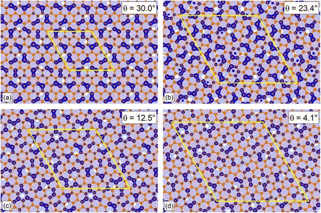
The left panels in Fig. 1 show the top view of G and CrI3 unit cells sharing the same hexagonal Bravais lattice. On an atomic basis, the G monolayer has two carbon atoms, whereas the CrI3 monolayer has two Cr and six I atoms, forming edge-sharing octahedra. We optimized the whole structures (atomic positions and lattice vectors) and obtained the lattice constants of aG = 2.45 Å and aCrI3 = 7.07 Å. The calculated lattice constants, aG and aCrI3, are in fair agreement with those reported for G37,38 and CrI312,39 monolayers. As a reference, the zigzag directions were extended parallel to the lattice vectors of both the G (carbon zigzag lines) and CrI3 (polyhedral zigzag lines) unit cells. Using the optimized unit cells, we employed the Nookiin software40 to build the four smallest commensurable G/CrI3 heterostructures, as shown in Fig. 1. Constraints of m ≥ n and p ≥ q were used to generate systems with θ values within the 0–30° range. In addition, the Nookiin software generated the integer pairs, (m,n) for G and (p,q) for CrI3, as shown in the first and third rows of Table 1. These sets of integers pairs are useful to define the corresponding transformation matrix for each hexagonal monolayer, PG and PCrI3:| |  | (1) |
 |
| | Fig. 1 Atomic models of (a) G (ball-and-stick) and (b) CrI3 (gray polyhedra) monolayers, and twisted magnetic heterostructures composed of G and CrI3 layers with (c) 30.0°, (d) 23.4°, (e) 12.5° and (f) 4.1°. C, Cr, and I atoms are presented in orange, silver, and purple colors. The yellow lines delimit the periodic cell. | |
Table 1 (m,n) and (p,q) integers to construct hexagonal commensurable SCs of G and CrI3. Integers pairs allow to define a G- and CrI3-periodicity. θ is the interlayer rotation angle (eqn (2)) in degrees, Δ is the biaxial strain (eqn (3)) percentage, and NT is the total number of atoms in the SC (eqn (4)). The (kx,ky) values of the equivalent KG and MG high-symmetry points of the G primitive cell (PC) in the reciprocal space of the heterostructure are reported. The total energy difference between the FM and AFM states, ΔEFM–AFM, is reported in meV per CrI3 unit cell. The exchange parameter value J is reported in meV per Cr ion
| (m,n)G |
(5,0) |
(6,4) |
(7,1) |
(9,2) |
|
G-periodicity |
5 × 5 |

|

|

|
| (p,q)CrI3 |
(1,1) |
(3,0) |
(2,1) |
(3,1) |
| CrI3-periodicity |

|
3 × 3 |

|

|
|
θ
|
30.0 |
23.4 |
12.5 |
4.1 |
|
Δ
|
+0.04 |
+0.70 |
−1.11 |
−2.45 |
|
N
T
|
74 |
224 |
170 |
310 |
|
K
G(kx,ky) |
5/3,5/3 |
2/3,14/3 |
2,3 |
7/3,13/3 |
|
M
G(kx,ky) |
5/2,0 |
3,2 |
7/2,1/2 |
9/2,1 |
| ΔEFM–AFM |
−85 |
−77 |
−87 |
−67 |
|
J
|
−3.15 |
−2.85 |
−3.22 |
−2.48 |
Besides, the integers m, n, p, and q were used for calculating the relative interlayer rotation angle (θ), the biaxial strain (Δ) on G, and the total number of atoms (Nt) in the twisted G/CrI3 heterostructures by:41,42
| |  | (2) |
| |  | (3) |
| | | Nt = 2(m2 + n2 + m·n) + 8(p2 + q2 + p·q). | (4) |
The calculated θ, Δ, and Nt values are presented in Table 1. As in previous reports, Fig. 1 shows that as the θ value decreases, the Nt value increases, or the moiré SC size also increases. For example, for the system with θ = 30.0°, a direct inspection shows that along the carbon zigzag lines of G, there are parallel armchair polyhedral lines from the CrI3 layer. The maximum θ value was 30° with an initial small expansion of Δ = +0.04% on the G layer and Nt = 74 atoms in the entire heterostructure. In contrast to the previous system, at θ = 4.1°, the heterostructure has Nt = 310 atoms, and the G layer undergoes an initial shrinkage effect of Δ = −2.45%. Let us mention that, since all the integer pairs are different from zero, except (5,0) for G and (3,0) for CrI3, the 2D transformation matrices defined in eqn (1) involve two symmetry operations on the monolayers, expansion and rotation, and we can define a general notation for lattice periodicity (reconstruction), as in the second and fourth rows of Table 1. Thus, the lattice periodicities of 5 × 5 for G and 3 × 3 for CrI3 involve only an expansion along the lattice vectors; see the systems with θ = 30.0° and 23.5° in comparison with the initial unit cell structures in Fig. 1. Additionally, the SC lattice constant can be calculated as the periodicity factor multiplied by the primitive lattice constant. For example, when θ = 4.1°, 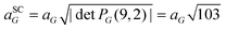 and
and 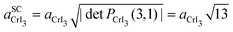 due to the hexagonal lattice symmetry of the SC.43 More data can be found in Table SI of the Supplementary Information (SI) for systems in which, despite the higher (m,n) and (p,q) integers, the θ values fall within the 19–28° range.
3.2 Electronic structure of pristine monolayers
The ground state electronic structure of G and CrI3 single layers are depicted in Fig. 2. The electronic band structure of G shows an already known linear dispersion around the K point at the Fermi energy owing to C(2pz) orbitals. Within this numerical DFT calculation, we found a hopping parameter tppπ ∼ 2.4 eV for C(2pz)–C(2pz) orbital interactions, giving a π-band which extends from 0 to ∼−7.2 eV, see Fig. S1(a) of the SI. The σ-bands composed of C(2s) and C(2px,y) orbitals start from ∼−3.5 eV and extend towards deeper energy values in the valence regime. The total density of states (DOS) of G shows a null value at 0 eV (Fermi energy), which is characteristic of the Dirac point in the band structure. In Fig. S1(b) of the SI, the total DOS increases linearly around 0 eV, with two van Hove singularities near −2 eV and −6.5 eV owing to the π-band and σ-bands, respectively.
 |
| | Fig. 2 Band structures along the directions connecting the high-symmetry points for non-magnetic (a) G and (c) FM CrI3 primitive cells and their corresponding normalized DOS in (b) G and (d) CrI3. The Fermi energy is set to 0 eV. For CrI3, the majority-spin and minority-spin contributions are colored with red and blue, respectively. | |
In contrast to the non-magnetic G layer, the CrI3 monolayer is a FM semiconductor with a single-spin narrow band gap by the majority-spin states around the Fermi energy. The calculated majority-spin direct band gap was ∼1 eV positioned at the Γ point. The obtained bandgap value is similar to 0.82 or 0.89 (1.19 or 1.23) eV in ref. 12 and 44, with Hubbard parametrization within the generalized gradient approximation with (without) the SOC term. Less dispersive electronic bands along the fully scanned k-path resemble the ionic bonding properties of an insulator. The hexagonal crystalline structure of the CrI3 monolayer has a point symmetry D3d. The crystal field induced by the I atoms splits with the Cr(3d) levels in an orbital triplet t2g and a higher energy doublet eg. Hence, the Cr(3d) levels of the Cr3+ ions should be occupied by three electrons, which occupy the single spin t2g triplet to minimize both orbital energy and Coulomb repulsion. However, the reported average magnetic moment >4μB in Table SIII (SI) is overestimated with the Mulliken charges in Table SII of the SI. Regarding the spin-resolved total DOS, the single unoccupied majority-spin states above the Fermi energy are a mixture of Cr(3d) and I(5p) orbitals,44 which, in our case, are separated from other single unoccupied minority-spin states at approximately 4 eV.
3.3 Spin-polarized graphene
In this section, we discuss the collinear magnetism induced on G by the CrI3 monolayer through the MPE. Once the ground state is achieved using the self-consistent method within SIESTA, we numerically calculate the local spin density σ(r) as follows45:where ρ↑(r) (ρ↓(r)) denotes the total majority-spin (minority-spin) charge density. Fig. 3 shows the four G/CrI3 heterostructures with a translucent plane positioned at the interface between the two layers to visualize only the minority-spin contributions located on the carbon atoms. Here, the unbalanced charge in C(2pz) orbitals allows a localized spin density. Note that, as θ decreases, the coverage of carbon atoms with local minority-spin contribution also decreases, as shown in Fig. 3. A high coverage of localized magnetic moments on carbon atoms was observed for high θ values. Several FM carbon pairs or triads are observed at θ = 30.0°, although only FM dimers are present with a few FM triads and some single FM atoms at θ = 4.1°. Tables SII and SIII in the SI show numerical values of total charge, Mulliken charges, and magnetic moments per cell and atom. Additionally, Fig. S2 in the SI shows the 2D spatial distribution of magnetic moments in G monolayers. Thus, a moiré-like induced collinear spin-polarized effect is observed in G in the real space. We expect these results to motivate experimentalists to study these G/CrI3 heterostructures to visualize single spin-polarized moiré states in G.15,21
 |
| | Fig. 3 Calculated local spin density in twisted G/CrI3 heterostructures with interlayer angles of (a) 30.0°, (b) 23.4°, (c) 12.5° and (d) 4.1°, where the yellow line denotes the periodic supercell. The blue color means minority-spin contributions in carbon atoms. Carbon atoms without a blue isosurface have an almost null local magnetization. | |
Second, we plot the partial DOS per spin for each heterostructure in the top panels of Fig. 4. After full optimization of the four G/CrI3 heterostructures, we found that the C(2pz) orbitals retain an electronic bandwidth of ∼−7.2 eV. The 2D quantum confinement of G can be observed from −7 eV to −5 eV with equal contributions from both spins. Furthermore, an asymmetric and oscillatory behavior is observed from −5 eV to 0.5 eV. As can be seen, linear dispersion is kept for minority-spin states above the Fermi energy and around the Dirac point, while the majority-spin states undergo energy broadening and enhancement induced by the CrI3 layer. Regarding the van Hove singularity positioned at −2 eV, attenuation plus a small energy spin-splitting is achieved as θ decreases. To enhance the effect of θ on the spin-polarized electronic states in G, we calculated the spin-polarization ratio (SPR),45 also known as the spin-filtering efficiency (SFE), using the results of the partial DOS shown in the top panels of Fig. 4. The SPR is calculated as follows:
| |  | (6) |
where DOS
↑[C(2p
z)] and DOS
↓[C(2p
z)] are the orbital-resolved DOS with majority-spin and minority-spin contributions, respectively. The SPR results are shown in the bottom panels of
Fig. 4. The moiré effect on the magnetic states of G can be observed mainly from −5 eV to 1 eV. Around the Fermi energy, electronic G states with majority-spin contributions tend to increase as
θ decreases, which is a positive SPR value, showing a narrow peak that not only increases from 45% to 70% but also has an up-shift in energy. From 0.5 to 1 eV and from 0 to −0.5 eV, we found regions with single-spin polarized states with minority-spin contributions. Also, note that a moiré effect is observed for unoccupied minority-spin states around 0.5 eV, plus an increase in the SPR of 10%. The complex oscillatory behavior in the SPR for energies lower than −1 eV is a clear fingerprint of the moiré effect in G/CrI
3 heterostructures. To end this section, we found SPR values on average less than 10% which slightly extended towards deep energies. This is shown for SPR values around −4.5 eV, as shown in
Fig. 4.
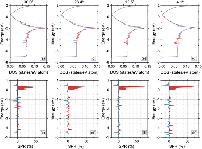 |
| | Fig. 4 Top panel: (a), (c), (e) and (g) show the average spin-polarized DOS for G C(2pz) orbitals. Red (blue) curves represent majority-spin (minority-spin) contributions. Bottom panel: (b), (d), (f) and (h) show the corresponding spin-polarization ratio (SPR), with positive (negative) values labeling majority-spin (minority-spin) contributions. In both panels, the Fermi energy is set to 0 eV. | |
3.4 Supercell band structure
In this subsection, we discuss the results of the SCs electronic band structures. Because the four G/CrI3 heterostructures maintain the hexagonal symmetry, we employed the following relative (or fractional) coordinates for the high-symmetry points in the irreducible SC Brillouin zone: γSC = (0,0), kSC = (1/3,1/3), and mSC = (0,1/2). The band structures per spin are shown in Fig. 5. In general, as the SC size or number of atoms increases, the SC system shrinks in reciprocal space, showing that several electronic states merge into the SC (mini) Brillouin zone, which is smaller than that of the original G or CrI3 PCs. This is due to the so-called ‘band-folding’ process of the electronic states.42 The folding mechanism usually provides a challenging interpretation of the physical results. In addition, this standard SC band structure result is not directly comparable to angle-resolved photoelectron spectroscopy (ARPES) measurements. Despite this, in this subsection, we focus on a small energy window around the Fermi energy to show that the low dispersive first conduction energy bands probably from the CrI3 monolayer are positioned just at the Fermi level. This indicates electron doping by charge transfer from the G layer, which is hole-doped. To observe the electron deficit in the G layer, we present a 2D plot of the atomic charges in the carbon atoms in Fig. S3 of the SI. However, in the energy window in Fig. 5, the CrI3 majority-spin contributions are mixed with those of the G monolayer, whereas the G minority-spin contributions remain non-perturbed. As in previous reports,37,41,46 whenever the SC G monolayer has a 3n total number of atoms, the high symmetry points KG and  of the G PC fold to the center of the SC Brillouin zone. In other words, the
  -points map towards the γ-point of the SC Brillouin zone. Hence, the band folding of
  is present in the G monolayer only for the G/CrI3 heterostructure with θ = 12.5° for both spin contributions. This is because the determinant of the matrix transformation, |det
![[thin space (1/6-em)]](https://www.rsc.org/images/entities/char_2009.gif) PG(7,1)| = 57 = 3 × 19, gives an integer number of three, whereas the other three G supercells probably have the next mapping,
PG(7,1)| = 57 = 3 × 19, gives an integer number of three, whereas the other three G supercells probably have the next mapping,  Additionally, it is worth mentioning that for θ = 12.5°, the two hole-doped and degenerate linear bands around the Dirac point have contributions from the KG and
  valleys from the G PC. And, at first sight, the G states close to Dirac points with the majority-spin states, red color in Fig. 5, hybridized directly with the CrI3 states at θ = 12.5° and 4.1°, whereas the other two systems with high θ = 30.0° and 23.4° did not.
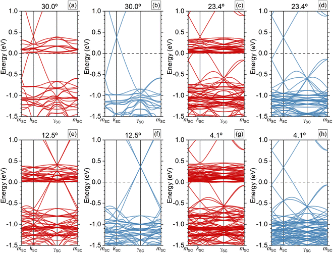 |
| | Fig. 5 Calculated supercell (SC) band structures of magnetic heterostructures with collinear spin-polarized states in (a), (c), (e) and (g) colored with red for majority-spin states, while in (b), (d), (f) and (h) with blue for minority-spin states. mSC, kSC, and γSC are the high-symmetry points defining the irreducible SC (mini) Brillouin zone. The Fermi energy is set to 0 eV. | |
3.5 Magnetic minigaps in graphene
In this section, we present the results of the spin-resolved unfolding method for periodic SCs in order to obtain an effective band structure per spin. Based on the stated computational methodology, the present results solely consider collinear spin interactions. This means that the Hamiltonian has the following form:| |  | (7) |
with the electron density for the majority ρ(r)↑ and minority ρ(r)↓ giving the total electronic density ρ(r) = ρ(r)↑ + ρ(r)↓ and the spin density in eqn (5). This allows Hamiltonian and electron decoupling, from which the spectral weight, WI(k),38,42 can be calculated separately for each spin contribution. Thus, by using the formalism described in ref. 42, we can define for each I-th band the majority-spin contributions as:| |  | (8) |
where the symbol ↑ represents the majority-spin states. The same  quantity can be defined for the minority-spin contributions. Here, the j labels all basis orbitals in space, while the I label is for different bands, and cI↑(k) corresponds to the complex coefficients from the Kohn–Sham orbitals obtained self-consistently taking collinear spins. Once the WI↑(k) calculation was performed, the results were deconvoluted using the following Lorentzian function:
| | 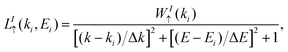 | (9) |
with smearing parameters Δk = 0.005 Å−1 and ΔE = 0.025 eV. Subsequently, we added all Lorentzian functions,  , and plot the results in Fig. 6. Note that the corresponding positions (relative to the reciprocal lattice vectors) of the high-symmetry points of the G PC, ΓG, KG and MG in the SC Brillouin zone were calculated. As an example for KG point, we have KG = kSC·PG. The new fractional positions of the symmetry points for the G monolayer are listed in Table 1. These theoretical results emulate the spin-resolved ARPES measurements of G/CrI3 heterostructures. First, Dirac cones with majority-spin contributions are positioned above the Fermi energy at the KG high-symmetry point. Several valence band discontinuities are observed for energy values less than −0.5 eV with the formation of spin-polarized minigaps. These spin-resolved minigaps, below −0.5 eV, were quantified and are shown in Fig. S4 of the SI. In general, these electronic minigaps have energy values larger than room temperature (25 meV). Therefore, the θ-dependence of the electronic structure of the G monolayer can be observed clearly around the KG for two perpendicular directions in reciprocal space.
 |
| | Fig. 6 Effective band structures projected onto the G PC with (a) 30.0°, (b) 23.4°, (c) 12.5° and (d) 4.1°. Only the majority-spin contributions around the KG point are plotted. The spectral weight, WI↑(k), is calculated for every electronic state. The dashed horizontal black line at 0 eV represents the Fermi energy. Blue arrows indicate the position of Dirac point. | |
The formation of narrow single-spin polarized bands in G monolayer was achieved at θ = 30.0° and 23.4° above Fermi energy. Conversely, the two G/CrI3 heterostructures with low θ exhibited parabolic bands near the Dirac point, as indicated by the blue arrows in Fig. 6. The electronic states with high spectral weights can be ascribed to the Dirac points of the G monolayer above the Fermi energy. These results are useful to determine the energy position of two Dirac points per spin and calculate a Zeeman-spin splitting energy, ΔZ(θ) = DP↑ − DP↓, with DP↑ (DP↓) denoting the energy position of majority-spin (minority-spin) Dirac point. The average results are ΔZ(θ) = +22, +24, +40 and −16 meV at θ = 30.0, 23.4, 12.5 and 4.1°, respectively. The positive Zeeman splitting could be correlated with an increase in the net magnetization of CrI3, which could increase the effective magnetic field on the carbon atoms, favoring electron polarization in the carbon atoms of G along the direction of the net magnetization of CrI3 (FM ordering in G). Note that pure FM ordering was observed at θ = 12.5°, where Zeeman splitting was at its maximum (see Fig. S2(c) of the SI). Conversely, the negative Zeeman splitting observed at θ = 4.1° increased the spin inversion, as shown in Fig. S2(d) of the SI. Thus, G exhibited small domains with AFM ordering. These outstanding results show twistable Zeeman-spin splitting with different values and signs. Finally, we clearly show the presence of magnetic minigaps in G, with different sizes and positions in energy, induced by the MPE of the CrI3 monolayer with different orientations. Therefore, the interlayer rotation angle θ is an additional degree of freedom to control the magnetic moiré states in G due to the MPE with the FM semiconductor CrI3 monolayer. It should be noted that external compression and electric fields, along with impurities, could be auxiliary knobs for tuning the electronic, magnetic, transport, topological and magnetoelectric properties,10,12,13,47 which deserves further study.
3.6 Atom and orbital contributions of CrI3
Fig. 7 presents the angle-dependent average atom- and orbital-resolved DOS of CrI3 based on the spin contribution. The FM state in CrI3 leads to an asymmetric energy behavior between the occupied majority-spin and minority-spin states from −5 to 0 eV. A downshift in the energy trend is observed as θ decreases. Less dispersive Cr(4s) states are positioned between −3.5 and −5 eV, and they do not contribute at the Fermi level. In the same valence regime, the Cr(4s) states were mixed with those of I(5s) and I(5p) orbitals. On the other hand, the mixing of Cr(3d) and mainly I(5p) orbitals extends from −4 eV to the Fermi energy. Notably, only the majority-spin Cr(3d) states contribute to this energy regime, and the minority-spin I(5p) orbitals generally prevail in the valence regime. Also, a majority-spin admixture of Cr(3d), I(5p), and I(5s) orbitals spans from the Fermi energy up to 0.5 eV, with the Cr(3d) and I(5p) orbitals predominating.
 |
| | Fig. 7 Average atom- and orbital-resolved density of states (DOS) for I and Cr atoms: (a) Cr(4s), (b) Cr(3d), (c) I(5s), and (d) I(5p) states. Red (blue) arrows denote majority-spin (minority-spin) contributions. The Fermi energy is set to 0 eV. | |
A more detailed analysis of the orbital-resolved DOS for the I(5p) orbitals per up (near to G) and down (far from G) layers is shown in Fig. 8. The iodine top (IT) and bottom (IB) layer represent the I orbital states that are closer to and farthest from the G monolayer. The perpendicular and degenerate in-plane electronic I states were attributed to I(5pz) and I(5px,y), respectively. In general, an increase in the bandwidth is obtained as the θ tends toward low values with attenuation for the majority-spin I(5pz) states close to the Fermi energy. The I(5px,y) in-plane states broaden more than I(5pz) to deeper energies because of bonding with I(4s) orbitals, as shown in Fig. 7.
 |
| | Fig. 8 Average orbital-resolved density of states (DOS) for I atoms: (a) IT(5pz), (b) IB(5pz), (c) IT(5px) = IT(5py), and (d) IB(5px) = IB(5py). The subscript T (B) labels the orbital contributions from I atoms nearer (farther) to the G monolayer. Red (blue) arrows denote majority-spin (minority-spin) contributions. The Fermi energy is set to 0 eV. | |
3.7 Magnetic exchange coupling
In addition to the novel and twistable electronic and magnetic properties of G induced by the MPE of the CrI3 monolayer, this section presents the results of the adjustable exchange coupling parameter J between the Cr spins due to the interfacial effect of the G monolayer. To obtain the J value, we first performed DFT calculations for two different magnetic configurations, a ferromagnetic (FM) state and another Néel antiferromagnetic (AFM) state (see Fig. S5 of the SI for more details) to obtain the corresponding total energy; and with these energy values, we then solve the next classical Heisenberg spin Hamiltonian:| |  | (10) |
where E0 is the total energy of the non-magnetic ground state, Ji,j is the exchange coupling term between the nearest-neighbor i and j sites, and Si (Sj) is the spin vector for each i (j) Cr atom. Because we found an overestimated local magnetic moment of the Cr atom in Table SIII of the SI, we adopt the ∼3.0μB44 value leading to a Cr atom with +3e charge and spin |Si| = 3/2. The total energy results for G/CrI3 systems show that the FM configuration is more stable than the Néel AFM configuration, with the energy difference ΔEFM–AFM = EFM − FAFM values reported in Table 1. Compared with the bare CrI3 monolayer with ΔEFM–AFM = −64 meV per unit cell, we found that the energy difference between the two magnetic configurations (FM and Néel-AFM) was lower and favored perpendicular FM alignment to the G/CrI3 heterostructure. The corresponding expression for the magnetic exchange interaction per Cr atom is J = ΔEFM–AFM/12|S|2 and the calculated values are shown in Table 1. First, all the J values are negative which means that the intralayer nearest-neighbor Cr–Cr coupling is FM, and indeed the J values for twisted G/CrI3 heterostructures are lower than the calculated value of J = −2.37 meV/Cr for the pristine CrI3 layer. Our calculated value J = −2.37 meV/Cr is in reasonable agreement with other reports.14,44,48–51 From this analysis, we expect that the Curie temperature TC = 45 K of the CrI3 monolayer4,52 will increase as in the 2D vdW CrPS4 magnet by the MPE owing to the monolayer G;53 but also, it will be twist-angle programmable.
4 Conclusions
In summary, we presented a detailed and systematic study of the building of periodic graphene/CrI3 heterostructures and then calculated the ground state structural, electronic, and magnetic properties using collinear spin-polarized DFT calculations. Four twisted heterostructures were built with maximal biaxial strain to avoid renormalization of the band structures and possible expansion, shrinkage, or corrugation of the graphene monolayer. Once the geometry was optimized, we found the same electronic bandwidth in graphene with a magnetic effect induced by ferromagnetic and semiconducting monolayers. Specifically, the maximum stress produces a reduction in the magnitude of the magnetic moments of carbon and favors spin reversal, giving rise to local AFM ordering in graphene. Clear fingerprints of the moiré effects are observed in the local spin density, spin-polarization ratio, orbital-resolved density of states and unfolded band structures for graphene, and an enhancement in the magnetic exchange coupling is observed in the CrI3 monolayer. Therefore, the interlayer rotation angle is an additional degree of freedom for the compression and electric fields to program the magnetic states in the vdW graphene/CrI3 heterostructures.
Author contributions
F. L. U. and F. S. O. contributed to conceptualization, formal analysis, investigation, methodology, supervision, validation, visualization, and writing – original draft.
Conflicts of interest
There are no conflicts to declare.
Note added after first publication
This PDF replaces the version published on 22 December 2025, which contained incorrect versions of eqn (9) and (10). The HTML version of the article is unaffected.
Data availability
The data supporting this article have been included as part of the supplementary information (SI). Supplementary information: tables with structural information (Table SI), atomic charges (Table SII) and magnetic moments (Table SIII); electronic properties of pristine graphene layer (Fig. S1); 2D maps of Mulliken atomic charges in graphene (Fig. S2) and resulting magnetic moments (Fig. S3); spin-resolved unfolded band structures with minigap values (Fig. S4); and top and side views of magnetic configurations in the CrI3 layer (Fig. S5). See DOI: https://doi.org/10.1039/d5tc03721b.
Acknowledgements
F. L. U. thanks SECIHTI (before CONAHCYT) through project 1564464-synergy and project CBF2023-2024-4119 (Ciencia Básica y de Frontera). F. S. O. acknowledges the financial support from SECIHTI (before CONAHCYT) grant no. CF-2023-I-336 and DGAPA-UNAM grant no. PAPIIT IA105623. Numerical calculations were performed in the Holiday cluster at the Physics Institute (UNAM). The authors thank Carlos Ernesto López Natarén for technical assistance.
References
- K. S. Novoselov, A. K. Geim, S. V. Morozov, D.-E. Jiang, Y. Zhang, S. V. Dubonos, I. V. Grigorieva and A. A. Firsov, Science, 2004, 306, 666–669 CrossRef CAS PubMed.
- I. Z. Žutić, J. Fabian and S. Das Sarma, Rev. Mod. Phys., 2004, 76, 323–410 CrossRef.
- A. Hirohata, K. Yamada, Y. Nakatani, I.-L. Prejbeanu, B. Diény, P. Pirro and B. Hillebrands, J. Magn. Magn. Mater., 2020, 509, 166711 Search PubMed.
- B. Huang, G. Clark, E. Navarro-Moratalla, D. R. Klein, R. Cheng, K. L. Seyler, D. Zhong, E. Schmidgall, M. A. McGuire and D. H. Cobden,
et al.
, Nature, 2017, 546, 270–273 Search PubMed.
- E. C. Ahn, npj 2D Mater. Appl., 2020, 4, 17 CrossRef CAS.
- Y. Liu, C. Zeng, J. Zhong, J. Ding, Z. M. Wang and Z. Liu, Nano-Micro Lett., 2020, 12, 1–26 CrossRef PubMed.
- C.-Z. Chang, W. Zhao, D. Y. Kim, H. Zhang, B. A. Assaf, D. Heiman, S.-C. Zhang, C. Liu, M. H. Chan and J. S. Moodera, Nat. Mater., 2015, 14, 473–477 CrossRef CAS.
- J. Jeong, D. H. Kiem, D. Guo, R. Duan, K. Watanabe, T. Taniguchi, Z. Liu, M. J. Han, S. Zheng and H. Yang, Adv. Mater., 2024, 36, 2310291 CrossRef CAS PubMed.
- C. Cardoso, D. Soriano, N. A. García-Martínez and J. Fernández-Rossier, Phys. Rev. Lett., 2018, 121, 067701 CrossRef CAS PubMed.
- M. U. Farooq and J. Hong, npj 2D Mater. Appl., 2019, 3, 3 CrossRef.
- I. Rozhansky and V. Fal'ko, Phys. Rev. Mater., 2024, 8, 074007 CrossRef CAS.
- J. Zhang, B. Zhao, T. Zhou, Y. Xue, C. Ma and Z. Yang, Phys. Rev. B, 2018, 97, 085401 CrossRef CAS.
- J.-T. Ren, Y. Feng, S.-S. Ke and H.-F. Lü, Adv. Phys. Res., 2025, 4, 2300026 CrossRef CAS.
- S. Bandyopadhyay, F. L. Buessen, R. Das, F. G. Utermohlen, N. Trivedi, A. Paramekanti and I. Dasgupta, Phys. Rev. B, 2022, 105, 184430 CrossRef CAS.
- Z. Qiu, M. Holwill, T. Olsen, P. Lyu, J. Li, H. Fang, H. Yang, M. Kashchenko, K. S. Novoselov and J. Lu, Nat. Commun., 2021, 12, 70 CrossRef CAS.
- C.-C. Tseng, T. Song, Q. Jiang, Z. Lin, C. Wang, J. Suh, K. Watanabe, T. Taniguchi, M. A. McGuire and D. Xiao,
et al.
, Nano Lett., 2022, 22, 8495–8501 CrossRef CAS PubMed.
- K. Zollner and J. Fabian, Phys. Rev. Lett., 2022, 128, 106401 CrossRef CAS PubMed.
- C. Tang, Z. Zhang, S. Lai, Q. Tan and W.-B. Gao, Adv. Mater., 2020, 32, 1908498 CrossRef CAS.
- S. K. Behera, M. Bora, S. S. P. Chowdhury and P. Deb, Phys. Chem. Chem. Phys., 2019, 21, 25788–25796 RSC.
- J. Zhang, B. Paulus, Y. Dedkov and E. Voloshina, J. Mater. Chem. C, 2025, 13, 11789–11799 RSC.
- M. Jugovac, I. Cojocariu, J. Sánchez-Barriga, P. Gargiani, M. Valvidares, V. Feyer, S. Blügel, G. Bihlmayer and P. Perna, Adv. Mater., 2023, 35, 2301441 CrossRef CAS.
- A. M. Holmes, S. Pakniyat, S. A. H. Gangaraj, F. Monticone, M. Weinert and G. W. Hanson, Phys. Rev. B, 2020, 102, 075435 Search PubMed.
- T. Naimer, K. Zollner, M. Gmitra and J. Fabian, Phys. Rev. B, 2021, 104, 195156 CrossRef CAS.
- N. Troullier and J. L. Martins, Phys. Rev. B, 1991, 43, 1993 Search PubMed.
- P. Ordejón, E. Artacho and J. M. Soler, Phys. Rev. B, 1996, 53, R10441 CrossRef.
- J. M. Soler, E. Artacho, J. D. Gale, A. Garca, J. Junquera, P. Ordejón and D. Sánchez-Portal, J. Phys.: Condens. Matter, 2002, 14, 2745 CrossRef CAS.
- R. Cuadrado and J. I. Cerdá, J. Phys.: Condens. Matter, 2012, 24, 086005 Search PubMed.
- O. A. Vydrov and T. van Voorhis, J. Chem. Phys., 2010, 133, 244103 CrossRef.
- S. L. Dudarev, G. A. Botton, S. Y. Savrasov, C. J. Humphreys and A. P. Sutton, Phys. Rev. B, 1998, 57, 1505–1509 CrossRef CAS.
- F. Haddadi, E. Linscott, I. Timrov, N. Marzari and M. Gibertini, Phys. Rev. Mater., 2024, 8, 014007 CrossRef CAS.
- I. V. Kashin, V. V. Mazurenko, M. I. Katsnelson and A. N. Rudenko, 2D Mater., 2020, 7, 025036 CrossRef CAS.
- Y. S. Hou, J. W. Kim and R. Q. Wu, Phys. Rev. B, 2020, 101, 121401 CrossRef CAS.
- V. Kumar Gudelli and G.-Y. Guo, New J. Phys., 2019, 21, 053012 CrossRef.
- H. J. Monkhorst and J. D. Pack, Phys. Rev. B, 1976, 13, 5188–5192 CrossRef.
- L. Bengtsson, Phys. Rev. B, 1999, 59, 12301–12304 CrossRef CAS.
- K. Momma and F. Izumi, J. Appl. Crystallogr., 2011, 44, 1272–1276 CrossRef CAS.
- Y. Betancur-Ocampo, S. Galván Y García, S. Tehuacanero-Nuñez, J. Reyes-Gasga, T. Stegmann and F. Sánchez-Ochoa, Phys. Rev. B, 2025, 111, 085431 CrossRef CAS.
- F. Sánchez-Ochoa, A. R. Botello-Méndez and C. Noguez, Phys. Rev. B, 2021, 104, 075430 CrossRef.
- C. Cardoso, A. T. Costa, A. H. MacDonald and J. Fernández-Rossier, Phys. Rev. B, 2023, 108, 184423 CrossRef CAS.
-
O. Aguilar-Espíndola, OssielAg/Nook-iin: Nook'iin: First public version, 2024, https://doi.org/10.5281/zenodo.14257397.
- F. Hidalgo, F. Sánchez-Ochoa and C. Noguez, npj 2D Mater. Appl., 2023, 7, 40 CrossRef CAS.
- F. Sánchez-Ochoa, F. Hidalgo, M. Pruneda and C. Noguez, J. Phys.: Condens. Matter, 2020, 32, 025501 CrossRef.
- O. Aguilar-Spíndola, A. Rubio-Ponce, F. López-Urías and F. Sánchez-Ochoa, Phys. Chem. Chem. Phys., 2025, 27, 11541–11550 RSC.
- Q. Yang, X. Hu, X. Shen, A. V. Krasheninnikov, Z. Chen and L. Sun, ACS Appl. Mater. Interfaces, 2021, 13, 21593–21601 CrossRef CAS PubMed.
- F. Sánchez-Ochoa, Phys. Rev. Appl., 2022, 18, 054068 CrossRef.
- S. G. y García, Y. Betancur-Ocampo, F. Sánchez-Ochoa and T. Stegmann, Nano Lett., 2024, 24, 2322–2327 CrossRef.
- X.-Q. Tian, A. Hassan, Y. Wang, Q.-F. Sun, X.-R. Wang, T. Altalhi, Y. Du and B. I. Yakobson, Adv. Funct. Mater., 2025, 2503185 CrossRef CAS.
- W.-B. Zhang, Q. Qu, P. Zhu and C.-H. Lam, J. Mater. Chem. C, 2015, 3, 12457–12468 RSC.
- H. Wang, F. Fan, S. Zhu and H. Wu, Europhys. Lett., 2016, 114, 47001 CrossRef.
- L. Chen, J.-H. Chung, T. Chen, C. Duan, A. Schneidewind, I. Radelytskyi, D. J. Voneshen, R. A. Ewings, M. B. Stone, A. I. Kolesnikov, B. Winn, S. Chi, R. A. Mole, D. H. Yu, B. Gao and P. Dai, Phys. Rev. B, 2020, 101, 134418 CrossRef CAS.
- W. Su, D. Wang, D. Wei and Z. Dai, Metals, 2025, 15, 398 Search PubMed.
- K. L. Seyler, D. Zhong, D. R. Klein, S. Gao, X. Zhang, B. Huang, E. Navarro-Moratalla, L. Yang, D. H. Cobden and M. A. McGuire,
et al.
, Nat. Phys., 2018, 14, 277–281 Search PubMed.
- W. Zhu, C. Song, L. Han, H. Bai, C. Chen and F. Pan, Phys. Rev. B, 2023, 108, L100406 Search PubMed.
|
| This journal is © The Royal Society of Chemistry 2026 |
Click here to see how this site uses Cookies. View our privacy policy here. 
 Open Access Article
 This Open Access Article is licensed under a
  a and
Francisco
Sánchez-Ochoa
a and
Francisco
Sánchez-Ochoa


 and
and  due to the hexagonal lattice symmetry of the SC.43 More data can be found in Table SI of the Supplementary Information (SI) for systems in which, despite the higher (m,n) and (p,q) integers, the θ values fall within the 19–28° range.


 of the G PC fold to the center of the SC Brillouin zone. In other words, the
  -points map towards the γ-point of the SC Brillouin zone. Hence, the band folding of
  is present in the G monolayer only for the G/CrI3 heterostructure with θ = 12.5° for both spin contributions. This is because the determinant of the matrix transformation, |det
 Additionally, it is worth mentioning that for θ = 12.5°, the two hole-doped and degenerate linear bands around the Dirac point have contributions from the KG and
  valleys from the G PC. And, at first sight, the G states close to Dirac points with the majority-spin states, red color in Fig. 5, hybridized directly with the CrI3 states at θ = 12.5° and 4.1°, whereas the other two systems with high θ = 30.0° and 23.4° did not.


 quantity can be defined for the minority-spin contributions. Here, the j labels all basis orbitals in space, while the I label is for different bands, and cI↑(k) corresponds to the complex coefficients from the Kohn–Sham orbitals obtained self-consistently taking collinear spins. Once the WI↑(k) calculation was performed, the results were deconvoluted using the following Lorentzian function:
 , and plot the results in Fig. 6. Note that the corresponding positions (relative to the reciprocal lattice vectors) of the high-symmetry points of the G PC, ΓG, KG and MG in the SC Brillouin zone were calculated. As an example for KG point, we have KG = kSC·PG. The new fractional positions of the symmetry points for the G monolayer are listed in Table 1. These theoretical results emulate the spin-resolved ARPES measurements of G/CrI3 heterostructures. First, Dirac cones with majority-spin contributions are positioned above the Fermi energy at the KG high-symmetry point. Several valence band discontinuities are observed for energy values less than −0.5 eV with the formation of spin-polarized minigaps. These spin-resolved minigaps, below −0.5 eV, were quantified and are shown in Fig. S4 of the SI. In general, these electronic minigaps have energy values larger than room temperature (25 meV). Therefore, the θ-dependence of the electronic structure of the G monolayer can be observed clearly around the KG for two perpendicular directions in reciprocal space.


