
 Open Access Article
 This Open Access Article is licensed under a
 Creative Commons Attribution 3.0 Unported Licence
Optoelectronic inhibitory synapses in the visible range from PbS nanocrystal arrays
Chrysi
Panagopoulou
 *a,
Panagiotis
Bousoulas
a,
Apostolos
Kalafatis
bc,
Spyros
Orfanoudakis
ab,
Charalampos
Tsioustas
a,
Alexandros
Banis
b,
Polychronis
Tsipas
b,
Athanassios G.
Kontos
ab,
Thomas
Stergiopoulos
*b and
Dimitris
Tsoukalas
a
*a,
Panagiotis
Bousoulas
a,
Apostolos
Kalafatis
bc,
Spyros
Orfanoudakis
ab,
Charalampos
Tsioustas
a,
Alexandros
Banis
b,
Polychronis
Tsipas
b,
Athanassios G.
Kontos
ab,
Thomas
Stergiopoulos
*b and
Dimitris
Tsoukalas
a
aSchool of Applied Mathematical and Physical Sciences, National Technical University of Athens, 15780 Athens, Greece. E-mail: chryssipanagopoulou@mail.ntua.gr
bInstitute of Nanoscience and Nanotechnology, NCSR Demokritos, 15341 Athens, Greece. E-mail: t.stergiopoulos@inn.demokritos.gr
cDepartment of Chemistry, National and Kapodistrian University of Athens, 15772 Athens, Greece
First published on 19th January 2026
Abstract
Optoelectronic inhibitory synapses play critical roles in modulating neural activity and maintaining the balance between excitation and inhibition within artificial neural circuits. However, most reported devices fail to properly emulate depression-related synaptic functions under optical stimulation. In this work, we demonstrate an optoelectronic inhibitory synaptic device based on lead sulfide (PbS) nanocrystals capped with iodide ligands. Crucially, the devices operate in the visible range (RGB), essential for retina-inspired color sensing, demonstrating inhibitory postsynaptic current (IPSC) behavior under 450, 550 and 740 nm illumination. A low power consumption of ∼40 nJ was also recorded under red light illumination. The system successfully emulates fundamental synaptic behaviors including paired-pulse depression (PPD), spiking-number-dependent plasticity (SNDP), and spiking-rate-dependent plasticity (SRDP), enabling biologically plausible visual processing.
The use of light into the design of optoelectronic memristors has lately garnered significant attention, emerging as a leading frontier in neurosynaptic device research.1 Since over 70% of human sensory information is derived from vision, the integration of light-stimulated optoelectronic synapses into artificial neural networks (ANNs) offers a cutting-edge platform for emulating the biological visual perception system and realizing neuromorphic biomimetic functionalities.1,2 To overcome the limitations of conventional computer architectures, photonic solutions for processing have evolved, offering a promising approach for enhanced computational performance.3 To this end, the development of robust optical synapses is considered of great importance.
Although the excitation of optical synapses with light pulses has been reported in many works in the literature,4–6 the inhibition remains a challenge and in most of the cases complex material configurations are used.7–14 Optical inhibition is particularly crucial in retinal-inspired neuromorphic systems, where it emulates the role of GABAA receptors in regulating lateral and feedback inhibition.15 This mechanism enables precise control over synaptic weight modulation in memristive devices, enhancing both network stability and adaptive information processing. Inhibitory synapses can generally be engineered to exhibit dynamic, tunable inhibition by adjusting light intensity, wavelength, or phase, mimicking the plasticity seen in biological systems.16,17 By enabling fast and energy-efficient inhibitory control, optoelectronic synapses hold promise for advancing real-time processing in applications, such as autonomous robotics, brain–computer interfaces, and sensory data interpretation.18
In this work, low power optoelectronic inhibitory synapses from ultra small nanocrystal arrays, namely lead sulfide (PbS), were fabricated and systematically examined. PbS is a common material, used for solar cells,19 photodetectors,20 transistors21,22 and memristors.23,24 The fabricated synapses were irradiated with optical pulses in the visible (RGB) range and a fully optical control of the synapse inhibition state was achieved. Our work provides valuable insights for the future fabrication of scalable artificial neural networks with accurate optoelectronic control of their synaptic properties.
Although the synthesis of PbS quantum dots (QDs) has been extensively studied and evolved for decades,25–27 their application into functional optoelectronic devices remains challenging. The most widely employed method for the synthesis of high quality QDs is the hot-injection reaction at an elevated temperature, where long aliphatic molecules (e.g., oleic acid, oleylamine, etc.) are used as surface ligands to control the nucleation and growth. Although these ligands are mandatory to produce high quality monodisperse QDs, they function as electrically insulating media hence hindering carrier transport in QD-based optoelectronic devices. To solve this problem, post-synthetic ligand-exchange strategies have been proposed to substitute the bulky ligands with shorter, more conductive ones. However, efficient ligand exchange in colloidal PbS QDs remains a challenge due to the Pb–Olate bond cleavage that usually leads to the formation of trap states.28 Recently, a direct synthetic approach was developed by the Ma group.29–32 This method completely circumvents the ligand exchange process and instead leverages an in situ surface passivation of the QD with iodide species. The final QDs are dispersed in polar solvents and offer superior efficiency.
The synthesis of PbS nanoparticles followed previous reports with adaptations.29,33 In a nitrogen filled glovebox, 4 mmol of lead iodide (PbI2, TCI, 99.99%) were dissolved in 5 mL of N,N-dimethylformamide (DMF, Thermo Fisher Scientific, 99%). To facilitate the dissolution the mixture was heated at 100 °C until a transparent yellow solution was obtained. Then, the solution was cooled down to room temperature and added to 1 mmol of N,N′-diphenylthiourea (DPTU, Thermo Fisher Scientific, 98%). The final solution was stirred at room temperature for 2 minutes and then 0.4 mL of n-butylamine (Thermo Fisher Scientific, 99+%) was swiftly injected, instantly forming a black colloid. The colloid was left to stir for 10 minutes before adding an excess amount of toluene (anhydrous, Thermo Fisher Scientific, 99.8%) (4![[thin space (1/6-em)]](https://www.rsc.org/images/entities/char_2009.gif) :1) to precipitate the nanoparticles and consequently centrifuged for 10 minutes at 6000 rpm to collect the solids. The solids were dried under vacuum and then redispersed in DMF with a concentration of 200 mg mL−1 for device fabrication.
:1) to precipitate the nanoparticles and consequently centrifuged for 10 minutes at 6000 rpm to collect the solids. The solids were dried under vacuum and then redispersed in DMF with a concentration of 200 mg mL−1 for device fabrication.
Transmission electron microcopy (TEM) images showed uniformly dispersed nanocrystals with an average size of 2.5–3 nm (Fig. 1c), indicative of strong quantum confinement. X-ray photoelectron spectroscopy (XPS) analysis (Fig. 1d) confirmed the presence of iodide through the I 3d spectrum (iii), while the Pb 4f (i) and S 2p (ii) spectra verified the chemical composition and oxidation states consistent with PbS. The presence of iodine peaks indicates successful ligand exchange and surface passivation.35 The X-ray diffraction (XRD) patterns (Fig. 1e) exhibited sharp peaks corresponding to the face-centered cubic phase of PbS, with no impurity phases detected. These results confirm the successful ligand exchange, high crystallinity, and structural purity of the QDs, making them promising for optoelectronic applications.
 | ||
| Fig. 1 Schematic illustration of (a) PbS with iodide ligands and (b) the fabricated device. (c) TEM plan view image of the PbS nanocrystals. The scale bar in (i) corresponds to 100 nm and to 20 nm in (ii). The inset shows a high-resolution image of a NC. (d) Pb 4f (i), S 2p (ii) and I 3d (iii) XPS spectra of PbS–I films with the corresponding peaks after fitting analysis. (e) XRD diffractogram of PbS. | ||
Interdigitated Ti (7 nm)/Au (75 nm) electrodes with a 10 µm gap were fabricated on top of Si/SiO2 (300 nm) substrates (Fig. S1b), using standard optical lithography and lift-off processes. The PbS layer was deposited by spin-coating PbS–I dispersion in DMF (200 mg mL−1) at 4000 rpm and dried in air at 70 °C for 5 minutes. The samples were measured by profilometry to have a thickness of approximately ∼350 nm, which is in good agreement with values reported in the literature.34Fig. 1a depicts the structure of the PbS NCs capped with iodide ligands; a schematic illustration of our device can be seen in Fig. 1b. The electrical measurements were conducted using a Keithley 4200-SCS semiconductor parameter analyzer. The triggering of the power LED array was conducted using the HP 8116A Pulse Generator.
Fig. 2a demonstrates the inhibitory postsynaptic current (IPSC) in response to a single 20 s optical pulse at wavelengths of 450 nm, 550 nm and 740 nm. As the wavelength increases, the photocurrent progressively decreases. This is because the photon energy diminishes with increasing wavelength, reducing the likelihood of electronic transitions across the energy bandgap. Additionally, the optical absorption coefficient generally decreases with wavelength, further contributing to the decline in photocurrent;36 this is also illustrated in the absorbance spectrum of Fig. S2. A shift from short-term memory (STM) to long-term memory (LTM) occurs with higher pulse width (Fig. 2b and c), as well as with increased pulse number (Fig. 2d–f), indicating the successful mimicking of the spike-width dependent plasticity (SWDP) and spike-number dependent plasticity (SNDP) of the proposed synaptic device.37 The post pulse current of Fig. 2b was also fitted with a decay function, which lead to the decay exponent increasing its value from 8.2 for the 1 s pulse to 27 for the 20 s optical pulse; thus, the STM to LTM was verified.
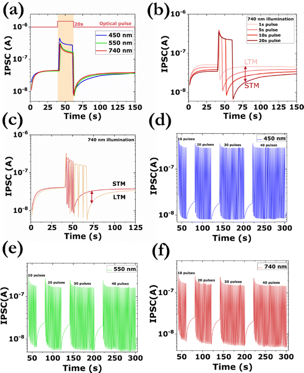 | ||
| Fig. 2 (a) IPSC response induced by a presynaptic optical pulse with a duration of 20 s for three different wavelengths with the same intensity of 1.22 mW cm−2. (b) Transition from STM to LTM under the application of single optical pulses with increasing duration for illumination of 740 nm. (c) Impact of the pulse width on LTM to STM transition for 740 nm irradiation. The red line corresponds to 5 pulses of 1 s width, while the yellow one refers to five 5 s-pulses. All IPSC responses were recorded at a read-out voltage of 1 V. (d)–(f) IPSC triggered by stimulus trains with different pulse numbers for three distinct wavelengths; 450 (d), 550 (e) and 740 nm (f) (frequency: 1 Hz, duration: 1 s). | ||
Paired-pulse depression (PPD) is a key synaptic plasticity property, characterized by a neurotransmitter-induced reduction in action potential, that serves as an important indicator of information processing at biological synapses. PPD behavior can be demonstrated by delivering two consecutive identical light pulses, with the second pulse eliciting a stronger inhibitory response than the first. The PPD index, defined as
 | (1) |
| PPD = C1exp(−t/τ) | (2) |
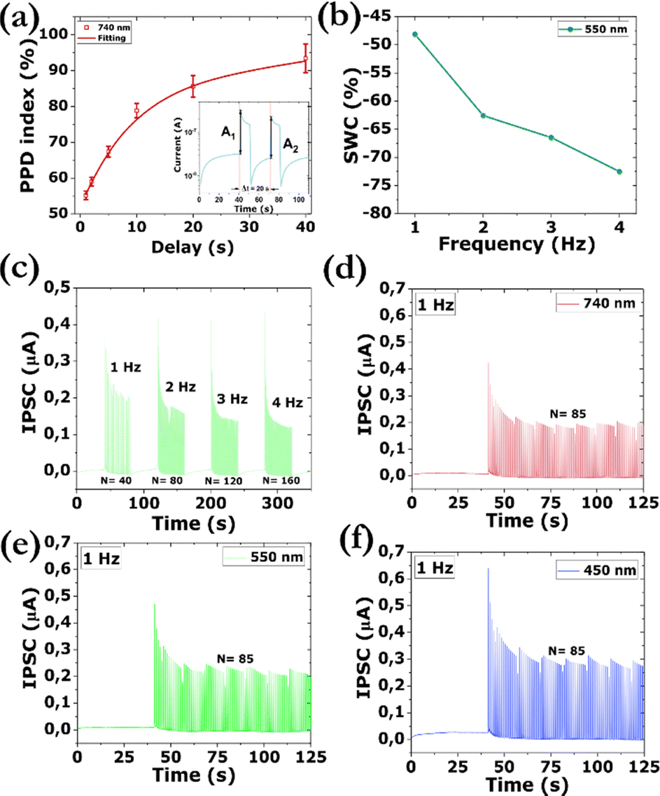 | ||
| Fig. 3 (a) Distribution of the PPD index as a function of the pulse interval (delay Δt) of the optical pulses. (b) The plot of synaptic weight via the pulse frequency for 550 nm light illumination (pulse width: 200 ms, intensity: 1.22 mW cm−2). (c) IPSC triggered by 4 consecutive trains of light pulses with different pulse frequencies (wavelength: 550 nm, duration: 200 ms) on a linear scale. N denotes the number of light pulses. (d)–(f) IPSC triggered by stimulus trains with three distinct wavelengths on a linear scale; 740 (d), 550 (e) and 450 nm (frequency: 1 Hz, duration: 200 ms, intensity: 1.22 mW cm−2). N refers to the number of light pulses. | ||
Another key characteristic of optoelectronic memristors lies in their capacity to modulate synaptic weight (conductance or resistance) in response to the intensity and frequency of incoming optical or electrical stimuli.1 The synaptic weight change (SWC), defined as
 | (3) |
Further validation is depicted in Fig. 3c, where synaptic event frequency was elevated when optical pulse frequency was increased from 1 to 4 Hz. Additional graphs of the SWC for red and blue irradiation are illustrated in Fig. S4.
The 450 nm optical pulse induced larger IPSC amplitudes compared to 550 and 740 nm stimulation, with synaptic weight changes exhibiting consistent wavelength-dependent trends. The same pattern held true under the application of a train of pulses with a duration of 200 ms, as illustrated in Fig. 3d–f, for a 1 Hz optical pulses’ frequency, as well as for shorter optical pulses of 100 ms (Fig. 4). In Fig. S5 the synthesis of PbS QDs via the hot-injection reaction with oleic acid (OA) shows no photoresponse during the irradiation of 450 nm light under the same conditions, verifying the insulating nature of these ligands. A low average energy consumption per spike of 40 nJ for red, 50 nJ for green and 55 nJ for blue light irradiation was calculated based on the following equation:
| Espike = V × I × tspike | (4) |
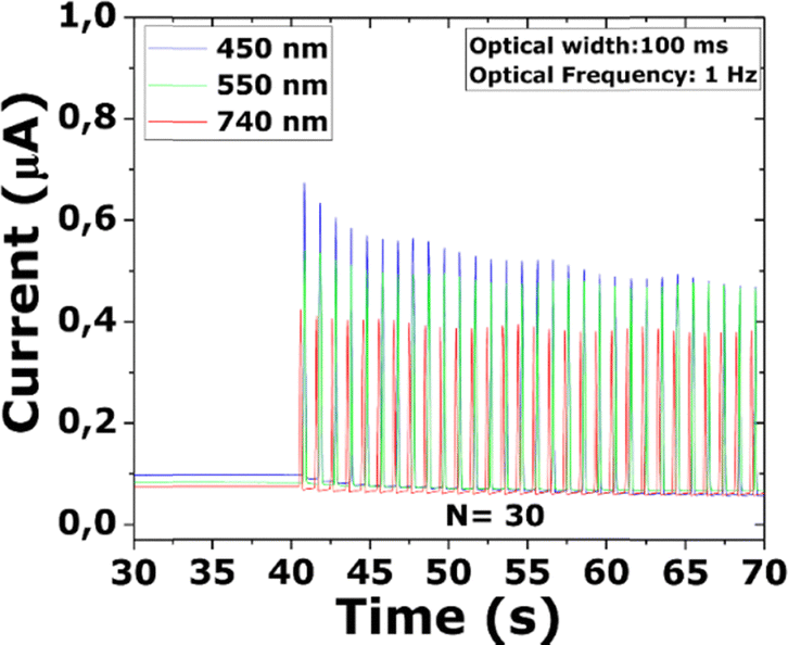 | ||
| Fig. 4 IPSC triggered by stimulus trains with three distinct wavelengths on a linear scale. The optical frequency of the irradiation was 1 Hz, while the optical width of the pulses was set to 100 ms. For all three wavelengths, the optical intensity was measured to be 1.22 mW cm−2. N refers to the number of light pulses. | ||
To understand the origins of the optoelectronic inhibitory behavior of our synaptic devices, we conducted ultraviolet photoelectron spectroscopy (UPS) characterization (Fig. 5a), based on which the energy band diagram of the PbS NCs–Au electrodes was constructed (Fig. 5b). Under RGB illumination, PbS NCs exhibit a characteristic photoresponse where initial photoexcitation generates excitons that dissociate into free carriers, producing a rapid current spike.41,42 Despite iodide passivation, residual traps (e.g., sulfur vacancies and electron trapping sites of silanol on the SiO2 surface) can capture photogenerated electrons over time with a higher rate than the photoexcitation;43–46 the initial peak current subsequently decays due to progressive trap-state filling, eventually reaching a steady-state balance between continuous carrier generation and trap-mediated losses. The observed decay time is attributed to the RC charging dynamics of the system, where the PbS NC network functions as a distributed capacitor, and a parallel resistive pathway models the leakage current between the electrodes through the percolating NC network. To quantitatively capture this behavior, the electrical response was modeled using a first-order resistor–capacitor (RC) circuit (LTspice), which reproduces the exponential charging and discharging dynamics (Fig. 5c); the agreement between experimental and simulated data under a 10 s optical pulse (740 nm) is shown in Fig. 5d. Although the nanocrystals exhibit strong quantum confinement with discrete energy levels, the equivalent RC circuit is employed as a phenomenological model to describe the macroscopic electrical relaxation behaviour. In particular, the first-order RC model effectively describes the charging and discharging dynamics of the nanocrystal ensemble as a whole, averaged over a large number of confined domains. Under small-bias and near-equilibrium conditions, the device shows a quasi-linear current–voltage response, justifying the use of a first-order linear approximation. The extracted RC parameters therefore represent the averaged charge transport and storage dynamics across the nanocrystal network, rather than the microscopic nonlinearities of individual confined states.
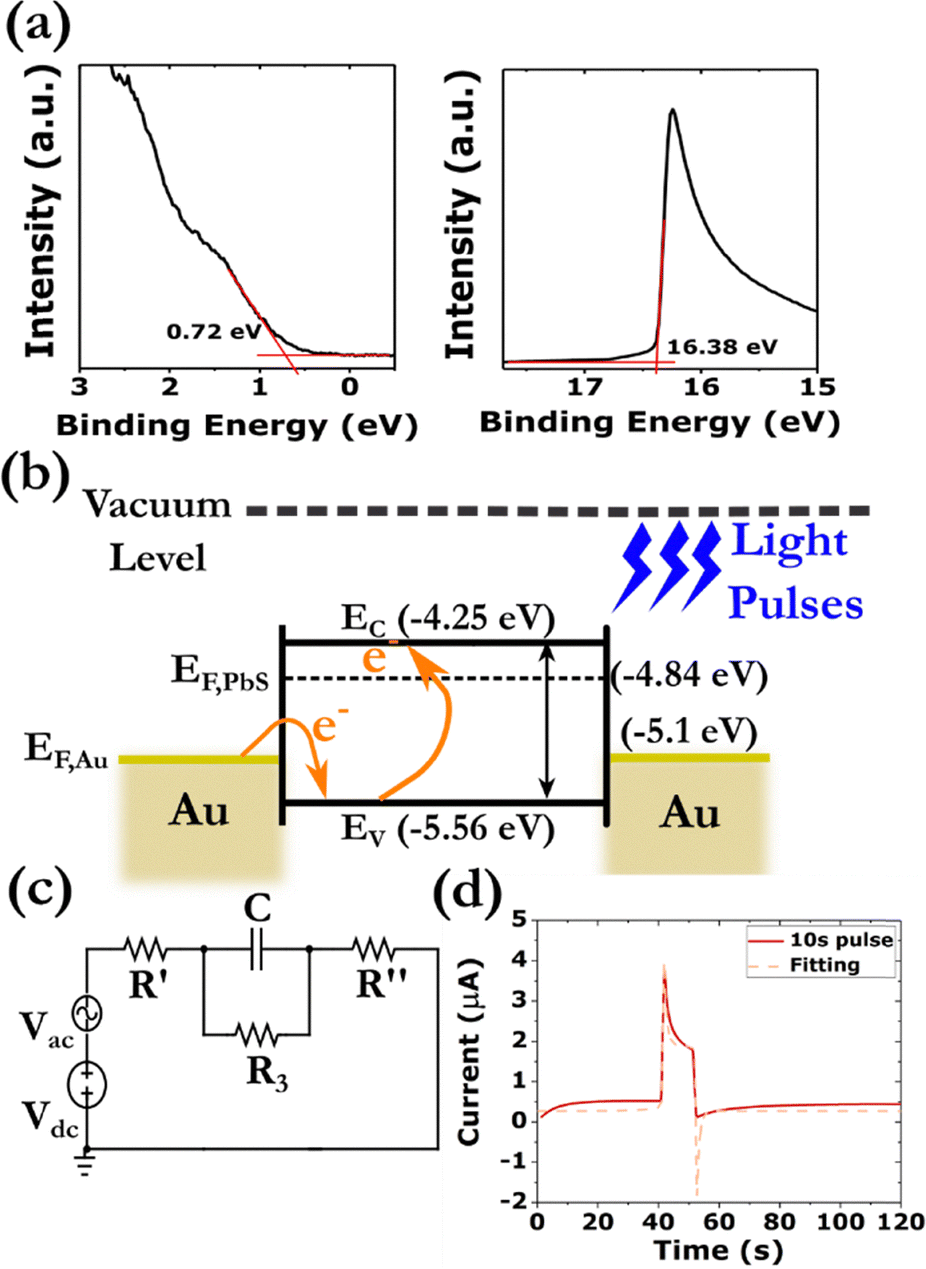 | ||
| Fig. 5 (a) UPS spectra of PbS film. (b) Energy band diagram of the PbS NCs–Au electrodes. (c) Equivalent circuit of the proposed device, which consists of the capacitance of the PbS NC network, connected in parallel to resistance R3 of the iodide ligands between the QDs. Gold electrodes are modeled as R′ = R1 + Rcontact and R″ = R2 + Rcontact, each equal to 6 MΩ. The electrode resistances reflect both the intrinsic series resistance of the interdigitated gold fingers (which is negligible) and the metal/semiconductor contact resistance. These values provide a realistic representation of the baseline device conductance prior to optical excitation and were used to define accurate boundary conditions for the circuit simulations. In the hybrid electro-optical setup, a Vdc bias of 1 V was applied electrically, while optical inputs were simulated as modulated pulses with an effective AC amplitude. During charging (irradiation Vdc = 1 V and Vac = 6 V were applied; during discharging, only the DC bias was maintained. The extracted capacitance value was 200 nF, and R3 was calculated as 25 MΩ. (d) Fitting between experimental (10 s pulse duration at 740 nm) and simulation data, according to the equivalent circuit model. | ||
When the light is turned off, the current initially drops rapidly as photoexcitation ceases, reaching a minimum value as trapped charges effectively screen the internal electric field, particularly at the PbS/SiO2 interface where holes tend to accumulate due to the insulating nature of the substrate. The subsequent exponential recovery of the current toward its initial dark current level, also denoted as the capacitive discharging time, is driven by the thermal release of trapped charges. Over time, carriers escape from shallow trap states through a thermally activated process, with the timescale governed by the trap depth and temperature according to an Arrhenius relationship.47,48 Simultaneously, charges accumulated at the PbS/SiO2 interface slowly leak back into the quantum dot layer, while the Schottky barrier at the Au/PbS contacts gradually relaxes as the screening effects diminish. This recovery process typically occurs on millisecond to second timescales, depending on the quality of the quantum dot passivation and the specific interface properties.49
Conclusions
In conclusion, this work tackles the key challenge of developing an optoelectronic inhibitory synapse tailored for the maintenance of excitation–inhibition balance within artificial neural circuits. We analysed the behavior of the device, which was based on lead sulfide (PbS) NCs capped with iodide ligands, in the visible range by implementing different synaptic schemes, such as PPD and SRDP, while achieving a low energy consumption in the range of 40–55 nJ. By harnessing interfacial chemistry at the nanocrystal level, we demonstrate a pathway to optoelectronic synapses that unite efficiency, tunability, and scalability, while also exhibiting a simple configuration scheme. In contrary to previously reported devices in the literature, our optoelectronic synapse achieved optical inhibition in three wavelengths of the retinal spectrum (RGB) (Table S1). This strategy opens new horizons for neuromorphic platforms, where chemical design principles directly dictate technological reach at the forefront of neuromorphic computing for autonomous systems with real-time sensory processing.Author contributions
Conceptualization: C. P., P. B., T. S. and D. T.; methodology: C. P., P. B., A. K., S. O., C. T., A. B., P. T., A. G. K.; formal analysis and data curation: C. P., P. B., A. K., S. O. and C. T.; writing – original draft preparation, C. P., P. B., A. K. and S. O.; writing – review and editing, C. P., P. B., A. K., S. O., T. S. and D. T.; supervision: A. G. K., T. S. and D. T.Conflicts of interest
There are no conflicts to declare.Data availability
Supplementary information is available. See DOI: https://doi.org/10.1039/d5tc03487f.Data for this article, including XPS, XRD, TEM and UPS characterization, as well as optoelectronic characterization, are available at open science framework repository, under the title “Optoelectronic inhibitory synapses in the visible range from PbS nanocrystal arrays” and identifier: DOI: https://doi.org/10.17605/OSF.IO/RW6Y3.
Acknowledgements
Four of the authors (C. P., P. B, C. T., D. T.) would like to acknowledge financial support for this work from the EU project ELEGANCE funded by the European Innovation Council and SMEs Executive Agency. This project has received funding from the HORIZON-EIC-2023-PATHFINDERCHALLENGES-01 call under grant agreement no 101161114. S. O. and T. S. would like to acknowledge financial support from the European Research Council (ERC) through the Consolidator Grant (818615-MIX2FIX). The work of S. O. has been also financially supported by the Hellenic Foundation for Research and Innovation (HFRI) under the 5th Call for HFRI PhD Fellowships (Fellowship Number: 19304).References
- J. Wang, N. Ilyas, Y. Ren, Y. Ji, S. Li, C. Li, F. Liu, D. Gu and K.-W. Ang, Adv. Mater., 2024, 36, 2307393 CrossRef CAS PubMed.
- R. Khan, N. Ur Rahman, M. Faisal Hayat, D. Ghernaout, A. A. M. Salih, G. Abbas Ashraf, A. Samad, M. Adil Mahmood, N. Rahman, M. Sohail, S. Iqbal, S. Abdullaev and A. Khan, Nanoscale, 2024, 16, 14589–14620 RSC.
- R. Li, Y. Gong, H. Huang, Y. Zhou, S. Mao, Z. Wei and Z. Zhang, Adv. Mater., 2025, 37, 2312825 CrossRef CAS PubMed.
- W. Zhou, R. Yang, H.-K. He, H.-M. Huang, J. Xiong and X. Guo, Appl. Phys. Lett., 2018, 113, 061107 CrossRef.
- Y.-X. Hou, Y. Li, Z.-C. Zhang, J.-Q. Li, D.-H. Qi, X.-D. Chen, J.-J. Wang, B.-W. Yao, M.-X. Yu, T.-B. Lu and J. Zhang, ACS Nano, 2021, 15, 1497–1508 Search PubMed.
- S. Cho, S. S. Kundale, J. Shim, S. Park, H. Kwak, A. V. Hoang, E.-T. Kim, S. Kim and J. H. Park, ACS Appl. Mater. Interfaces, 2025, 17, 6460–6472 CrossRef CAS PubMed.
- C.-M. Yang, T.-C. Chen, D. Verma, L.-J. Li, B. Liu, W.-H. Chang and C.-S. Lai, Adv. Funct. Mater., 2020, 30, 2001598 Search PubMed.
- S. W. Cho, S. M. Kwon, Y.-H. Kim and S. K. Park, Adv. Intell. Syst., 2021, 3, 2000162 CrossRef.
- Z. Shen, C. Zhao, L. Kang, Y. Sun, Y. Liu, I. Z. Mitrovic, L. Yang, E. G. Lim, Z. Zeng and C. Zhao, Adv. Intell. Syst., 2022, 4, 2100236 CrossRef.
- D. Rao, A. I. K. Pillai, M. Garbrecht and B. Saha, Adv. Electron. Mater., 2023, 9, 2200975 CrossRef CAS.
- M. Cui, P. Zhao, C. Jiang, B. Tian, C. Luo, H. Lin, H. Peng and C.-G. Duan, ACS Appl. Electron. Mater., 2023, 5, 3403–3409 CrossRef CAS.
- C. Zhu, T. Guo, H. Zhang, J. Jiang, Z. Lin, X. Wei, L. Wang, X. Liu, X. Li, X. Yu and W. Huang, J. Mater. Chem. C, 2025, 11671–11683 Search PubMed.
- R. Yang, D. Hu, Q. Chen, Z. Wang, B. Lu, Z. Ye, X. Li and J. Lu, Adv. Funct. Mater., 2025, 35, 2414210 CrossRef CAS.
- W. Huang, S. Jiang, Z. Lin, X. Zhang, H. Fei, J. Jiang, J. Tang, X. Zhang, X. Yu and L. Wang, Appl. Phys. Rev., 2025, 031401 Search PubMed.
- J. Nagy, B. Ebbinghaus, M. Hoon and R. Sinha, eLife, 2021, 10, e60994 CrossRef CAS PubMed.
- S. Ebert, T. Buffet, B. S. Sermet, O. Marre and B. Cessac, Nat. Commun., 2024, 15, 6118 CrossRef CAS PubMed.
- F. Zhang, C. Li, Z. Li, L. Dong and J. Zhao, Microsyst. Nanoeng., 2023, 9, 16 CrossRef PubMed.
- Y. Kim, C. W. Lee and H. W. Jang, J. Electron. Mater., 2025, 54, 3609–3650 CrossRef CAS.
- Y. Cao, A. Stavrinadis, T. Lasanta, D. So and G. Konstantatos, Nat. Energy, 2016, 1, 16035 CrossRef CAS.
- F. Fang, Y. Tang, H. Tang, Y. Song, Q. Chen, L. Rao, S. Xiao, W. Chen and L. Cao, ACS Appl. Electron. Mater., 2025, 7, 7368–7376 CrossRef CAS.
- K. Shibata, M. Yoshida, K. Hirakawa, T. Otsuka, S. Z. Bisri and Y. Iwasa, Nat. Commun., 2023, 14, 7486 CrossRef CAS PubMed.
- T. Feng, H. Xu, Y. Yang, X. Hu, T. Wang, H. Zhu, Q. Sun, D. W. Zhang, J. Meng and L. Chen, Nano Lett., 2025, 25, 3637–3645 CrossRef CAS PubMed.
- J. Lin, Z. Wang, Q. Lin, J. Sun, X. Guo, Y. Wang, L. Lin, Y. Zhao, Y. Liu and D. Li, J. Phys. Chem. Lett., 2024, 16, 199–208 CrossRef PubMed.
- X. Lin, Z. Lin, W. Zhao, S. Xu, E. Chen, T. Guo and Y. Ye, Appl. Phys. Lett., 2025, 126, 263503 CrossRef CAS.
- M. A. Hines and G. D. Scholes, Adv. Mater., 2003, 15, 1844–1849 Search PubMed.
- B. Yuan, T. K. Egner, V. Venditti and L. Cademartiri, Nat. Commun., 2018, 9, 1–7 Search PubMed.
- C. Ding, D. Wang, D. Liu, H. Li, Y. Li, S. Hayase, T. Sogabe, T. Masuda, Y. Zhou, Y. Yao, Z. Zou, R. Wang and Q. Shen, Adv. Energy Mater., 2022, 2201676 CrossRef CAS.
- M. Liu, O. Voznyy, R. Sabatini, F. P. García de Arquer, R. Munir, A. H. Balawi, X. Lan, F. Fan, G. Walters, A. R. Kirmani, S. Hoogland, F. Laquai, A. Amassian and E. H. Sargent, Nat. Mater., 2017, 16, 258–263 Search PubMed.
- Y. Wang, Z. Liu, N. Huo, F. Li, M. Gu, X. Ling, Y. Zhang, K. Lu, L. Han, H. Fang, A. G. Shulga, Y. Xue, S. Zhou, F. Yang, X. Tang, J. Zheng, M. Antonietta Loi, G. Konstantatos and W. Ma, Nat. Commun., 2019, 10, 5136 CrossRef PubMed.
- Y. Liu, Y. Gao, Q. Yang, G. Xu, X. Zhou, G. Shi, X. Lyu, H. Wu, J. Liu, S. Fang, M. I. Ullah, L. Song, K. Lu, M. Cao, Q. Zhang, T. Li, J. Xu, S. Wang, Z. Liu and W. Ma, Angew. Chem., Int. Ed., 2023, e202300396 CAS.
- L. Yuan, Y. Li, Y. Liu, K. Lu, G. Shi, X. Sun, Y. Li, X. Dong, Y. Xiao, L. Huang, Z. Liu and W. Ma, Angew. Chem., Int. Ed., 2025, e202416369 Search PubMed.
- X. Ding, X. Wen, Y. Kawata, Y. Liu, G. Shi, R. ben Ghazi, X. Sun, Y. Zhu, H. Wu, H. Gao, Q. Shen, Z. Liu and W. Ma, Nanoscale, 2024, 16, 5115–5122 Search PubMed.
- Y. Liu, Y. Gao, Q. Yang, G. Xu, X. Zhou, G. Shi, X. Lyu, H. Wu, J. Liu and S. Fang, Angew. Chem., Int. Ed., 2023, 62, e202300396 Search PubMed.
- Y. Liu, Y. Gao, Q. Yang, G. Xu, X. Zhou, G. Shi, X. Lyu, H. Wu, J. Liu and S. Fang, Angew. Chem., Int. Ed., 2023, 62, e202300396 Search PubMed.
- Y. Wang, Z. Liu, N. Huo, F. Li, M. Gu, X. Ling, Y. Zhang, K. Lu, L. Han, H. Fang, A. G. Shulga, Y. Xue, S. Zhou, F. Yang, X. Tang, J. Zheng, M. Antonietta Loi, G. Konstantatos and W. Ma, Nat. Commun., 2019, 10, 5136 CrossRef PubMed.
- H. Wu, Z. Liu, B. Wang, L. Zheng, S. Lian, J. Zhang, S. Zhang, G. Zhang, Z. Xue, S. Yang, X. Cheng, G. Ding, Z. Liu, C. Ye and G. Wang, ACS Photonics, 2024, 11, 1342–1351 CrossRef CAS.
- S. G. Kim, Q. Van Le, J. S. Han, H. Kim, M.-J. Choi, S. A. Lee, T. L. Kim, S. B. Kim, S. Y. Kim and H. W. Jang, Adv. Funct. Mater., 2019, 29, 1906686 CrossRef CAS.
- R. S. Zucker and W. G. Regehr, Annu. Rev. Physiol., 2002, 64, 355–405 Search PubMed.
- L. F. Abbott and W. G. Regehr, Nature, 2004, 431, 796–803 CrossRef CAS PubMed.
- B. Chen, S. Sun, S. Fan, X. Liu, Q. Li and J. Su, Adv. Electron. Mater., 2022, 8, 2200864 Search PubMed.
- I. Ka, V. Le Borgne, K. Fujisawa, T. Hayashi, Y. A. Kim, M. Endo, D. Ma and M. A. El Khakani, Sci. Rep., 2016, 6, 20083 Search PubMed.
- J. Gao and J. C. Johnson, ACS Nano, 2012, 6, 3292–3303 Search PubMed.
- Z. Jin, A. Wang, Q. Zhou, Y. Wang and J. Wang, Sci. Rep., 2016, 6, 37106 Search PubMed.
- J. Hu, X. He, H. Pu, Y. Yang and C. Chen, Superlattices Microstruct., 2020, 145, 106616 Search PubMed.
- A. A. Bakulin, S. Neutzner, H. J. Bakker, L. Ottaviani, D. Barakel and Z. Chen, ACS Nano, 2013, 7, 8771–8779 Search PubMed.
- M. I. Nugraha, R. Häusermann, S. Z. Bisri, H. Matsui, M. Sytnyk, W. Heiss, J. Takeya and M. A. Loi, Adv. Mater., 2015, 27, 2107–2112 CrossRef CAS PubMed.
- H. Zhao, H. Liang, F. Vidal, F. Rosei, A. Vomiero and D. Ma, J. Phys. Chem. C, 2014, 118, 20585–20593 CrossRef CAS.
- G. Konstantatos and E. H. Sargent, Appl. Phys. Lett., 2007, 91, 173505 CrossRef.
- V. Gray, J. R. Allardice, Z. Zhang, S. Dowland, J. Xiao, A. J. I. Petty, J. E. Anthony, N. C. Greenham and A. Rao, ACS Nano, 2020, 14, 4224–4234 CrossRef CAS PubMed.
| This journal is © The Royal Society of Chemistry 2026 |