
 Open Access Article
 This Open Access Article is licensed under a
 Creative Commons Attribution 3.0 Unported Licence
Mechanistic insights into the dry oxidation of amorphous silicon nitride: a DFT study
Lukas
Hückmann
 a,
Robert
Sylvia
a,
Floris
Blankenvoorde
a,
Jonathon
Cottom
abc and
Jörg
Meyer
*a
a,
Robert
Sylvia
a,
Floris
Blankenvoorde
a,
Jonathon
Cottom
abc and
Jörg
Meyer
*a
aLeiden Institute of Chemistry, Gorlaeus Laboratories, Leiden University, P.O. Box 9502, 2300 RA, Leiden, The Netherlands. E-mail: j.meyer@chem.leidenuniv.nl
bAdvanced Research Center for Nanolithography, Science Park 106, 1098 XG, Amsterdam, The Netherlands
cInstitute for Theoretical Physics, University of Amsterdam, Science Park 904, Amsterdam, 1098 XH, The Netherlands
First published on 27th October 2025
Abstract
Amorphous silicon nitride (a-Si3N4) is vital for modern nanoelectronics, serving as dielectric layers, diffusion barriers, and charge-trapping layers in flash memory devices. From a thermodynamic viewpoint, a-Si3N4 is prone to oxidation, which can compromise the material's properties. However, experimental studies suggest that kinetic barriers largely prevent the reaction from proceeding at a rapid pace. In this study, we provide new insights based on DFT calculations into the role of oxygen defects in a-Si3N4, revealing that their perturbation of the local structure can create shallow trap sites. However, these traps compete with native trap precursors and rather stem from structural distortion than from oxygen itself – unlike in the crystalline phase. To elucidate the oxidation resistance, we calculate the barriers connecting interstitial and substitutional defects, which suggests that successive nitrogen replacement necessitates the concerted breaking of Si–N bonds facilitated by a local oxygen excess. The formidable oxidation resistance of a-Si3N4, as well as the experimentally observed NO2(g)![[thin space (1/6-em)]](https://www.rsc.org/images/entities/char_2009.gif) :NO(g) ratio exhibiting an unexpectedly high abundance of NO(g), is thereby rationalised.
:NO(g) ratio exhibiting an unexpectedly high abundance of NO(g), is thereby rationalised.
1 Introduction
Amorphous silicon nitride (a-Si3N4) is an essential material for nanoelectronics, valued for its mechanical properties,1,2 thermal stability,3 chemical resistance,4,5 high dielectric constant,6,7 and wide band gap.8 Among its most notable characteristics is its ability to trap charges over extended periods,9,10 which underpins its application in non-volatile flash memory devices.11–15 These devices rely on the controlled injection and removal of electrons via applied external voltages for information storage. The mechanism of charge trapping in a-Si3N4 is attributed to dangling silicon bonds, referred to as K-centres, which were first identified by Robertson and others through electron paramagnetic resonance (EPR) experiments.16–20 Injected electrons are hypothesised to occupy low-lying, empty states localised on silicon atoms with unsaturated coordination (K-centres), a concept subsequently supported by computational studies.21–26 To enable the controlled manipulation of charge carriers, such devices are typically constructed as multilayer stacks, incorporating a-Si3N4 as the charge-trapping layer between a tunnelling oxide and a blocking oxide. Common architectures include SONOS (Si/SiO2/Si3N4/SiO2/Si) and TANOS (TaN/Al2O3/Si3N4/SiO2/Si) stacks.15,27–31 Beyond their traditional role in charge-trapping memories, silicon nitride and related oxynitrides have also emerged as key active layers in resistive random-access memory (ReRAM) and memristive devices, where their defect-mediated conductivity and switching dynamics enable non-volatile resistance modulation.32–34Oxygen impurities play an important role in the performance of silicon nitride-based devices. It has been established by numerous experimental studies that silicon oxy-nitride (SiNxOy) or oxygen-doped a-Si3N4 films exhibit distinct properties compared to pristine a-Si3N4.35–40 With increasing oxygen content, the band gap of the material widens from approximately 4.5 eV in pristine a-Si3N4 to about 5.2 eV at an oxygen concentration of 40%. Simultaneously, gap states associated with dangling Si bonds shift by 0.15 eV, settling at 3.12 eV above the valence band maximum (VBM). Additional gap states, attributed to Si–O–Si and N–Si–O configurations near the valence band edge are observed.41–43 The incorporation of oxygen further reduces the trap density and shifts the distribution of trap states to shallower energy levels. This leads to an increase in charge carrier diffusivity, which can promote lateral and vertical leakage, negatively impacting data retention.44 Conversely, the presence of shallower states reduces hysteresis in capacitance–voltage (CV) measurements, facilitating easier memory write and erase operations. As a result, the advantages and disadvantages of SiNxOy remain a topic of ongoing debate.32–34,40,45–47
Experimentally, it is proposed that oxygen compensates for K-centres by occupying deep-lying states, with oxygen's additional electron (compared to nitrogen) playing a key role. Grillo et al.48 modelled oxygen substitutional defects (ON) in crystalline β-Si3N4 and demonstrated that these defects introduce mid-gap states slightly above those associated with K-centres. Oxygen donates one electron to lower-lying states, replacing a Si-centered two-electron trap with a one-electron oxygen-centred trap (ON → ON+ + e−). More recently, Bermudez49 confirmed these findings, showing that ON in β-Si3N4 donates an electron to the surface, indicating that the surface offers a more stable site to accommodate an excess electron over the ON defect. Whether these results are transferable to the amorphous phase remains an open question due to the inherent distortion present, which offers a wide range of intrinsic and defect-based traps and, therefore, potentially a qualitatively different behaviour of mid-gap states.24,25,50
The mechanisms underlying oxygen incorporation into a-Si3N4 remain elusive. From a thermodynamic perspective, SiO2 is favoured over Si3N451–53 according to net reaction54
| Si3N4(s) + 3O2(g) → 3SiO2(s) + 2N2(g) | (1) |
 ). The well-documented and often quoted oxidation resistance of a-Si3N4 is attributed to its kinetic rather than thermodynamic stability. This resistance may be compromised in nascent, highly defective a-Si3N4 films, where oxygen incorporation can occur during deposition processes, particularly under high-temperature annealing of oxide–nitride stacks.55,56 Additionally, mobile oxygen57 can migrate from oxide substrates into the nitride under applied voltage in operational devices, forming a mixed oxide–nitride phase at the interface.48,54,58–61 Mechanistic insights into the mode of oxidation of a-Si3N4 have been gained through extensive studies employing Rutherford backscattering spectroscopy (RBS).51,52,62 When a-Si3N4 thin films are exposed to dry oxygen atmospheres at elevated temperatures, a two-stage oxidation process is observed: an initial rapid surface oxidation followed by the slower, gradual growth of a SiO2 layer from the surface downward. While this process superficially resembles the oxidation of crystalline silicon (α-Si + O2 → SiO2), which is modelled by the Deal–Grove framework,63 it deviates significantly in detail. The Deal–Grove model accounts for three key steps: (1) the transport of O2 to the surface, (2) the diffusion of O2 through the growing oxide layer, and (3) a first-order reaction at the Si/SiO2 interface. However, earlier studies noted that this model fails to capture the oxidation kinetics of a-Si3N4, particularly the disproportionately rapid surface oxidation and the unusually slow bulk oxidation.62,64–67 A plausible explanation is that the diffusion of N2 gas from the reaction site counteracts the ingress of O2.62,64,68 Recent work by Wang et al.69 provides additional evidence, showing that the gaseous products consist of both N2 and NOx species. This finding implies a more complex reaction mechanism, as the formation of N2 is thermodynamically much more favourable than that of NO or NO2, suggesting that the observed outcomes are governed by kinetic factors rather than thermodynamics alone.
In this study, we systematically investigate how oxygen incorporates into a-Si3N4 by focusing on interstitial and substitutional sites as key intermediates in the oxidation process. Building up on our previous work to decipher the interplay between point defects50 and native charge traps70 in a-Si3N4, we exhaustively sample possible incorporation sites in the amorphous network. After analysing structural and electronic characteristics of these defects, we have also redone earlier calculations for oxygen defects in β-Si3N448,49 using our computational setup to consistently compare and discuss similarities and differences between the crystalline and amorphous phases. Finally, we establish a connection between individual interstitial and substitutional defect states by calculating reaction pathways that involve the formation of N2(g) and NO(g), both in the dilute limit and under oxygen-rich conditions. The resulting minimum energy paths reveal how the interplay of the amorphous network's topology, thermodynamics and kinetic barriers governs the oxidation of a-Si3N4. These insights provide a first step for understanding the oxidation mechanism in amorphous silicon nitride at the atomic scale. We discuss implications for nano-electronic applications, including potential strategies to control oxygen-induced defect formation.
2 Methods
All DFT calculations were performed spin-polarised in CP2K71 with the DZVP-SR-MOLOPT72 basis set for the valence electrons and the GTH pseudopotentials73,74 to account for the core electrons. The energy cut-off was set to 650 Ry and the relative cut-off to 70 Ry, and the Brillouin zone was sampled by a single k-point (Γ-point). The convergence criterion for the SCF procedure was 1 × 10⁻⁷ eV for the energy and 0.005 eV Å−1 for the forces. Geometry optimizations were performed with the quasi-Newton BFGS scheme.75–78 All structures were initially pre-optimised with the PBE functional79,80 followed by optimisation with the HSE0681,82 hybrid functional to ensure an accurate description of the defect states relative to the valence band maximum (VBM) and conduction band minimum (CBM). Atom-projected density of states and Mulliken charges83 have been extracted for the analysis of defect-induced states and semi-quantitative trends of charge transfer.In amorphous materials, it is of crucial importance to adequately sample the vast amount of defect configurations associated with the configurational space of the host material. Here, we adapt the approach presented50 and successfully employed70,85 in our earlier work, for which the computational workflow is depicted in Fig. 1: we start from the structural ensemble for a-Si3N4,86 which has been generated using a melt-quench procedure (step 1) and consists of validated simulation cells each containing 280 atoms (step 2). Then we select a single, representative cell from this ensemble to provide a common reference for all samples, thus allowing to disentangle the defects from a broad range of native intrinsic trap levels (steps 3 and 4). For the oxygen substitution defects (ON), each of the 160 nitrogen atoms in the cell was individually replaced with an oxygen atom. For the interstitial defects, we adapt the sampling approach of our previous work70 using Voronoi tessellation to confine the sampling space while maintaining statistical significance (step 5). Interstitial atoms (Ni or Oi) have been placed at the largest face of the Voronoi polyhedron, provided that the distance to its nearest neighbour was at least 2 Å in accordance with the radial distribution function50 to avoid artificial disruption of bonds in dense configurations. This procedure yielded a total of 240 interstitial sites, where oxygen atoms are initially placed in the local cavities next to their reference atoms and are allowed to relax without any constraints during the ensuing DFT calculations. After geometry optimizations at the PBE level for all Oi and ON defects, a subset of 50 structures each was selected such that the distributions of formation energies and structural motifs of the large (PBE-based) set are reproduced. 50 Ni structures have then been generated based on the Oi subset. This allows us to sample the configurational space with HSE06 in an efficient, statistically consistent manner (see Section S1 in the SI for further details).
 | ||
| Fig. 1 Flowchart describing the sampling of oxygen defects in a-Si3N4: an ensemble of structures is generated using the MG2 interatomic potential84 and structures were optimised with PBE, see ref. 50 (steps 1 and 2). From this ensemble, a single, representative sample has been selected to model the defects (steps 3 and 4). The exhaustive sampling of defects has been done using Voronoi tessellation (step 5) as previously in ref. 70. Finally, structural optimisation and electronic property analysis were performed using HSE06 (step 6). The flowchart is largely adapted from ref. 85. | ||
Defect formation energies have been calculated following the approach originally suggested by Zhang and Northrup:87
 | (2) |
Screening different charge states (q = {−1,0,+1}) revealed that the valence band maximum and the conduction band minimum are determined by native defects in a-Si3N4 and apart from very few outliers are not affected by oxygen (see SI). In other words, charge-transition levels are solely dependent on the VBM/CBM states in the dilute limit—similar to what is observed for hydrogen defects.70 Consequently, the charge state is kept to 0 for all calculations.
To make the link between the isolated point defects and the oxidation reaction, the transition from Oi defects to Si–O–Si configurations, three reaction pathways are calculated to examine the formation of N2, N2 under oxygen excess, and NO, each starting from a minimum of five different defect sites. The nudged elastic band (NEB) method90–92 has been employed, using a spring constant of k = 0.02 Ha Bohr−2. To suppress spurious charge transfer at the intermediate configurations along the NEB, the intrinsic trap sites were frozen. The NEB paths were converged with PBE followed by HSE single-point calculations for each image to obtain an energy profile and barriers.
3 Results
It is well established that oxygen migrates into the nitride layer when oxides are deposited on a-Si3N4 at elevated temperatures.48,60 In addition, the application of bias during device operation can induce Frenkel pairs in a-SiO2, consisting of oxygen vacancies and mobile oxygen interstitials.57,93 Hence, in devices based on SONOS architectures, oxygen interstitials (Oi) are the primary reactive species, serving as the vector of oxidation in a-Si3N4 devices. This motivates focusing on the following sub-steps for the oxidation reaction described by eqn (1):1. Formation of a substitution defect: an oxygen interstitial replaces a nitrogen atom, forming an ON defect with a dangling Si atom (Si˙) and a nitrogen interstitial (Ni):
| N(–Si)3 + Oi → Si–ON–Si + Si˙ + Ni | (3) |
2. Conversion of the nitrogen interstitial: the Ni converts into a mobile molecular species, such as N2
| 2Ni → N2, | (4) |
| Ni + xOi → NOx. | (5) |
Consequently, to elucidate the behaviour of oxygen in a-Si3N4, the results are organised as follows: Sections 3.1–3.3 describe the individual static defect configurations for Oi, ON, and Ni, examining their geometries, electronic structures, and formation energies. Section 3.4 quantifies the barriers for transitioning from Oi to ON, both in the dilute limit and under excess oxygen conditions. We distinguish between the formation of N2(g) and NO(g) as both products are conceivable under oxygen excess and in fact, NOx∈{1,2} species have been detected by Wang et al.69 However, since the formation of higher nitric oxides would require more severe restructuring of the amorphous network and NO2 is probably formed via intermediate NO anyway, the models presented here will be restricted to NO(g).
3.1 Oxygen interstitials (Oi)
As described in eqn (2), all oxygen interstitials are initially placed adjacent to the Si and N atoms with a threshold distance of 2 Å to prevent their artificial insertion in the amorphous network. We have classified the results of the DFT geometry optimizations based on their relaxed bond topology. A broad set of the initial geometries collapses into one of three classes (Fig. 2a–c): | ||
| Fig. 2 Examples for the oxygen interstitial configurations in a-Si3N4: (a) Si–O–Si bridges, (b) nitroxy bridges, and (c) oxygen interstitials. Silicon is coloured yellow, nitrogen is blue, and oxygen is red. Averaged values for bond lengths and angles of the respective defect type are marked in these images. (d) Distribution P of the bond lengths rOi–X of oxygen atoms to its nearest neighbours. For comparison, the Si–O bond length in α-quartz88 (α-SiO2, dashed line), the Si–N bond length in β-Si3N489 (dotted line), and the Oi–X bond lengths in crystalline β-Si3N4 (solid line) are added. (e) and (f) Distribution of formation energies Eform the Mulliken charges (qmul) of the three defect types. | ||
(a) Si–O–Si bridges (OSiOSii), where oxygen inserts between two Si atoms displacing the N atom, leaving either a dangling nitrogen or a five-fold coordinated silicon atom (19%),
(b) nitroxy bridges (ONOSii), where the oxygen inserts into a Si–N bond forming a Si–N–O–Si bridge (53%), and
(c) “true” oxygen interstitials (Oi), where the interstitial atom interacts with a Si–N pair but does not interrupt the bond between them or cause any other noteworthy modification of the amorphous network (28%).
Additional analysis of the joint fingerprints are provided in Fig. S5 in the SI.
In the case of OSiOSii-bridges, the oxygen's local environment is reminiscent of that in SiO2. Yet, the average bond length (1.71 Å) and angle (119.8°) resemble somewhat those of nitrogen atoms in a-Si3N4 – in contrast to the 1.61 Å bonds and the 140° to 150° angles found in a-SiO2 (see Fig. 2d).88,94 Thus, the rigidity of the amorphous network prevents the OSiOSii site from fully relaxing into an SiO2-like configuration. Nevertheless, they exhibit the lowest formation energy, averaging −1.34 eV with a notable spread from −2.61 eV to 0.84 eV (Fig. 2e). This behaviour can be understood in terms of the electronic structure: when adding a neutral oxygen atom, formally, a two-electron deficiency is introduced. The Mulliken charge (qmul) on the OSiOSii atoms indicate a high degree of polarisation with on average −0.56e suggesting that oxygen is present as O2− (Fig. 2f). In the simplest case, this is facilitated by the formation of a bipolaron at the native hole trap in the a-Si3N4 sample. However, this compensation is not always possible due to the displaced N atom. In general, it is sufficient to break only one Si–N bond to displace the N atom, allowing the resulting dangling N to form a five-fold coordinated Si to be readily accommodated by the surrounding network. Problems arise when the local structure hinders such rearrangement, leading to the formation of a new N-centre and an associated defect state in the band gap. Depending on the relative energy levels of the new N-centre and the native ones, two spatially separated single hole polarons are created as depicted in Fig. 3a and d. In extreme cases, the O atom is also involved (Fig. 3b and e), manifesting itself in an oxygen-centred, non-occupied state in the middle of the band gap. Such an electronic structure is unfavourable and explains the presence of OSiOSii sites with high Eform and the substantial spread thereof.
 | ||
| Fig. 3 The projected electronic density of states (DOS) relative to the Fermi level EF of (a) two spatially separated single hole polarons localising on the Oi atom and on the emerging N-centres, (b) an Oi atom in a OSiOSii configuration that does not achieve electronic saturation forming a mid-gap state, and (c) an Oi, that affects neither the VBM nor the CBM. Si is yellow, N is blue, and O is red, with an amplification of factor 10 for visibility. (d)–(f) Depiction of structures and Kohn–Sham states belonging to the labels in the DOS plots (a)–(c). The green/purple states represent the α channel being localised on the native trap site, and the blue/red states represent the β channel localising on the N-centre/Oi atom. | ||
For the other two defect types, the situation is markedly different. Both ONOSii and Oi exhibit an O–N bond with an average length of 1.45 Å and 1.50 Å, respectively. The average Si–O–N bond angles are notably sharp, i.e., 108.3° for ONOSii and 73.7° for Oi (see Fig. 2b and c). Evidently, the amorphous network is stable enough at these sites to prevent oxygen from significantly modifying the local structure or from inserting into a bond. Consequently, the polarisation of the O atom and its neighbouring N atom is considerably lower with only −0.36e for O and −0.26e for N (compared to the average charge on nitrogen of −0.54e). Furthermore, the native hole traps remain fully occupied, as indicated by the density of states shown in Fig. 3c and f. Oxygen does not contribute to mid-gap states, which is why it is not susceptible to accepting additional electrons. Combining these findings with the aforementioned reduced Mulliken charges suggests that Oi and ONOSii withdraw electron density directly from its neighbouring N and Si, which leads to a weakly polar, covalent interaction between N and O. Such an arrangement is energetically less favourable with Eform being 0.62 eV and 1.23 eV, respectively.
In conclusion, the various Oi defects underscore the tendency of a-Si3N4 to oxidize, reflecting the fact that Si–O bonds are stronger than Si–N bonds. However, the rigidity in the amorphous network and the formidable Si–N bonds allow the direct incorporation of oxygen only if there is a suitable site a priori available, resulting in a continuous gradation from non-disruptive Oi defects to silica-like OSiOSii structures. That encompasses not only the local structure and bonding situation but also the electronic structure, transitioning from rather polar-covalent N–O–Si bonds to more ionic Si–O–Si bonds.
3.2 Oxygen substitutions (ON)
As discussed earlier, oxygen substitution defects (ON) are considered to be the end point of the oxidation reaction to replace nitrogen in the amorphous network (see eqn (3)). A representative example of an ON defect in a-Si3N4 is provided in Fig. 4a. Similarly to the OSiOSii defects, the ON–Si bond lengths are 1.73 Å and are accompanied by bond angles of 120.24° on average. The aforementioned rigidity of the Si3N4-network also applies here, preventing the ON from achieving an ideal silica-like structure. Looking at bond length distributions (see Fig. 4b) illustrates that the amount of bond lengths ranging from 1.60 Å to 1.65 Å increases upon substitution, evidencing a certain degree of local relaxation. Fig. 4c shows that the defect formation energies are spread over a wide range from −4.33 eV to 0.69 eV with an average of −1.26 eV. There is an approximately linear relation between Eform and the cumulative displacement (||Δr||). The negative slope suggests that more pronounced local deformation of the amorphous network is energetically favoured. While there is thus a formidable thermodynamic driving force to achieve a silica-like configuration, major structural modifications in a-Si3N4 are not observed in the dilute limit.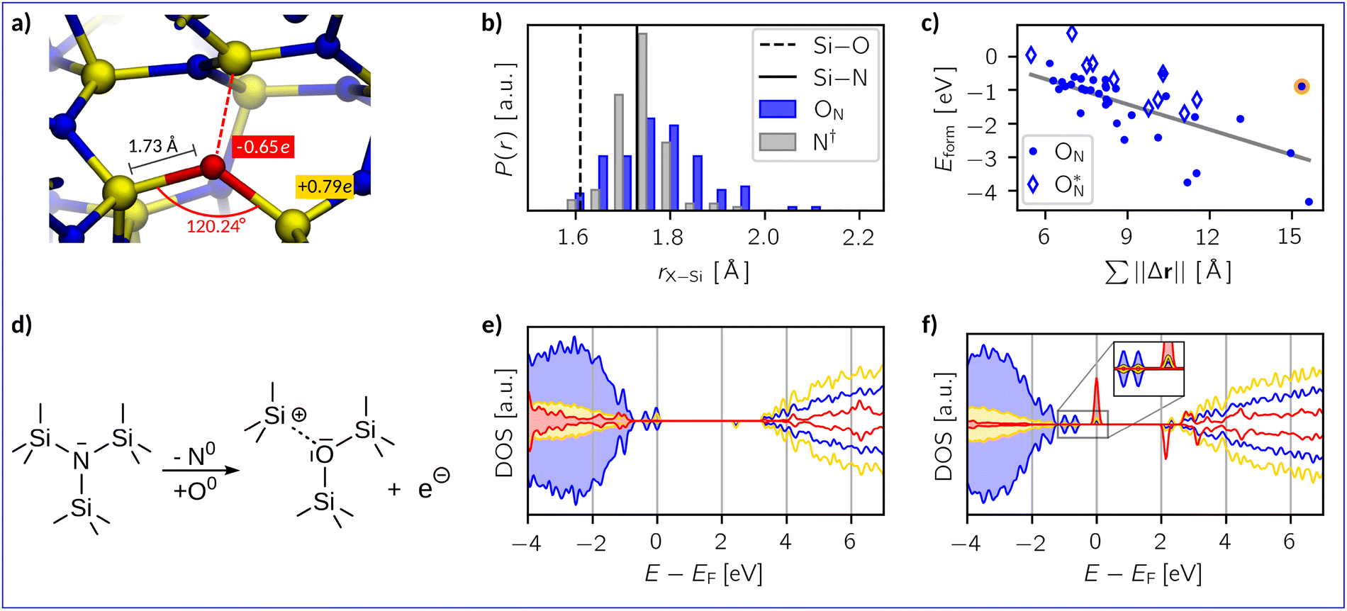 | ||
Fig. 4 (a) A representative example structure of an ON defect in a-Si3N4. Averaged values for Si–O bond lengths, Si–ON–Si-bond angles and Mulliken charges associated with Si and O atoms are indicated. (b) Distribution of X–Si bond lengths r of the substitution site before (N†, grey) and after oxygen incorporation (ON, blue). For comparison, the Si–O bond length in α-quartz88 (black-dashed line) and the Si–N bond length in β-Si3N489 (black-solid line) shown. (c) Eform as function of the cumulative displacement of atoms 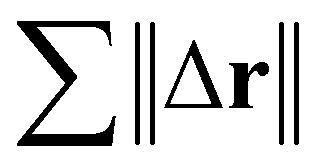 caused by the oxygen substitution. Hollow diamonds represent structures where oxygen contributes to mid-gap states and the orange-labelled data point marks an outlier. (d) Schematic representation of the oxygen substitution. (e) and (f) The projected electronic density of states (DOS) relative to the Fermi level EF of Si (yellow), N (blue), and O (red). The O-projected DOS is amplified by a factor of 50 for visibility. caused by the oxygen substitution. Hollow diamonds represent structures where oxygen contributes to mid-gap states and the orange-labelled data point marks an outlier. (d) Schematic representation of the oxygen substitution. (e) and (f) The projected electronic density of states (DOS) relative to the Fermi level EF of Si (yellow), N (blue), and O (red). The O-projected DOS is amplified by a factor of 50 for visibility. | ||
The second important aspect in the context of electronic devices is the impact of oxygen on the electronic structure. As schematically depicted in Fig. 4d, the introduction of a neutral ON defect adds one excess electron and creates a dangling Si bond, which can be understood as 1/3 of a nitrogen vacancy (1/3VN, see Fig. 4a). This structural motif is reminiscent of the K-centres, that are attributed to electron trapping in a-Si3N4. However, a detailed analysis of spin moments reveals that in 80% of the samples the excess electron still localises on the native electron trap in a-Si3N4 (see SI, Fig. S4b). The zero spin moment on the SiN3 unit within the 1/3VN indicates that the coulombic interaction of the nearby ON defect stabilises the (formal) Si4+ state, preventing it from taking up the excess electron and therefore it does not act as a new K-centre. Thus, oxygen does not contribute to the electronic states close to the VBM or CBM, as further illustrated by the density of states in Fig. 4e. Similar to what is observed for hydrogen defects,70 the charge transition levels and associated electronic properties remain dictated by the pristine a-Si3N4.
In the remaining 20% of the samples, the SiN3 relaxes in such a way that allows trapping an electron on the new K-centre, resulting in a N3Si–SiNx∈{3,4}-dumbbell type electron trap50,95 with participation of ON in the electronic state in the band gap (Fig. 4f). The associated formation energies, denoted as  in Fig. 4c are notably lower with −0.68 eV on average, hinting towards the increased presence of shallow traps in SiNxOy due to the presence of oxygen as reported in literature.
3.3 Isolated nitrogen interstitials (Ni)
The complete oxidation reaction (see eqn (1)) requires removing nitrogen from the amorphous network of a-Si3N4. As shown in Section 3.1, the insertion of oxygen atoms as interstitial defects creates a nitrogen interstitials, which remain firmly bound to the a-Si3N4 network. In this section, we analyse in detail whether this behaviour differs for isolated nitrogen interstitials (Ni) that are not in the vicinity of Oi.
Fig. 5 illustrates the two principal incorporation patterns of Ni in a-Si3N4. In both cases, the Ni atom inserts into an Si–N bond, forming a Si2N–NiSi2 structure. Henceforth, these configurations will be referred to as nitrogen insertions (Nins). The key distinction between them is whether Nins shares a silicon atom with its neighbouring nitrogen. That results in either a C3-like coordination environment similar to that of native N atoms (46%, Fig. 5a) or in a Nins–N–Si triangular-shaped arrangement (38%, Fig. 5b). The remaining 16% (labelled as  in Fig. 5d) follow the same patterns but lack a third Si neighbour for the Nins atom. As shown in Fig. 5c, with an average of 1.79 Å the Nins–Si bond lengths are not particularly unusual—only slightly elongated over the equilibrium Si–N bond. In contrast, the Nins–N bond spans 1.33 Å to 1.67 Å, which is notably longer than the N
![[triple bond, length as m-dash]](https://www.rsc.org/images/entities/char_e002.gif) N bond found in molecular N2 (1.11 Å with HSE) and is instead comparable to N–N single bonds found in weakly polar, covalent species like N2H496 and exotic transition metal nitrides like PtN2 and CrN2.97–99 Accordingly, the polarisation on both of the Nins atom and its adjacent N neighbour is reduced (to −0.25e and −0.31e, respectively) compared with that of non-involved N atoms (−0.54e), see SI.
N bond found in molecular N2 (1.11 Å with HSE) and is instead comparable to N–N single bonds found in weakly polar, covalent species like N2H496 and exotic transition metal nitrides like PtN2 and CrN2.97–99 Accordingly, the polarisation on both of the Nins atom and its adjacent N neighbour is reduced (to −0.25e and −0.31e, respectively) compared with that of non-involved N atoms (−0.54e), see SI.
 | ||
Fig. 5 Examples for nitrogen interstitial configurations inserting in a Si–N bond (Nins) in a-Si3N4 with (a) Nains exhibiting a broken C3 environment and (b) Nbins sharing a neighbouring Si with its adjacent N atom. For both types, the mean Nins–N and Nins–Si bond lengths are provided. (c) Distribution of the bond lengths rNins−X of Nins to its nearest neighbours. (d) Distribution of formation energies Eform for the different Nins defects, with results for Nains and Nbins shown in blue and orange, respectively. The red bars are other Nins-type defects  that are discussed in more detail in the text. The upper and lower x-axes use 1/2N2(g) and N0(g) as a reference for Eform, respectively. that are discussed in more detail in the text. The upper and lower x-axes use 1/2N2(g) and N0(g) as a reference for Eform, respectively. | ||
This unusual structural arrangement is reflected in the wide spread of formation energies (Fig. 5d). When referencing against ½N2(g), Eform is positive for all Nins sites, ranging from 0.53 eV to 6.44 eV with an average of 3.07 eV. In other words, nitrogen molecules are thermodynamically highly favoured over Nins defects, which is not surprising as the NN bond is inherently stable. Nevertheless, the necessity of breaking multiple Si–N bonds does not allow for the spontaneous formation of N2, as such a process is not observed in any of the samples. When referencing Eform against the chemical potential of a neutral N atom in vacuum the abscissa in Fig. 5d shifts by half the binding energy of N2(g) (4.42 eV in our HSE06 calculations, in good agreement with comparable literature values100). This renders Eform negative for most of the Nins configurations, making them favoured over unbound nitrogen atoms. Despite the peculiar insertion patterns, Nins strongly binds to the amorphous network, precluding it from diffusing away from the insertion site. Therefore, converting nitrogen into a mobile species, which is capable of moving freely through a-Si3N4 to ultimately leave it in gaseous form, is essential to complete the total oxidation reaction.
3.4 Reaction pathways for oxygen substitution in a-Si3N4
To study complete pathways of oxygen incorporation into a-Si3N4, we combine and connect the different defect configurations discussed above. Starting from Oi or ONOSii defects as reactant states, we calculate minimum energy paths (MEP) for them to transition to ON, thereby gradually displacing N and provoking Ni formation, see eqn (3). As discussed in Section 3.3, interstitial nitrogen binds strongly to the amorphous network, i.e. it is not chemically intuitive how the Ni atoms can be “mobilized” (eqn (4) and (5)). The following three reaction pathways for the removal of Ni are studied:(a) The direct formation of molecular N2(g) from Ni and a neighbouring N atom resulting in the formation of a nitrogen vacancy (VN ≙ 3Si˙).
(b) The formation of N2(g)via the concerted substitution of two Oi in close proximity.
(c) The formation of NO(g) with a (second) Oi defect adjacent to the emerging Ni atom.
The steps for the ON formation and the removal of Ni are visualised in Fig. 6a–c, respectively. Metastable intermediates occurring due to the rugged PES of the amorphous phase are omitted to focus the presentation on the decisive elementary steps. For each reaction pathway, a minimum of five different defects forming the reaction sites were examined. The reaction sites were selected such that
 | ||
| Fig. 6 Ball-and-stick model together with the respective energy profiles of the oxidation via an oxygen interstitial (Oi) forming (a) O2 and a nitrogen-vacancy (VN), (b) N2 with a second Oi, and (c) NO with an adjacent second Oi. There is one outlier in path (c) labelled with a cyan diamond; further discussion is provided in the text. Silicon is coloured in yellow, nitrogen in blue, and oxygen in red. N atoms that are involved in the reactions are highlighted in teal. Atoms in the amorphous network that are not involved in the reaction are omitted to focus the view. (d)–(f) The projected density of states (DOS) relative to the Fermi level (EF) for the product states of the reaction paths a, b, and c, respectively. The colour code is the same as for the atoms, and the O-projected DOS amplified by a factor of 10 in each panel. | ||
(i) all types of oxygen interstitials are included in the sampling,
(ii) too densely packed regions are avoided, since these paths hinder the formation of N2(g) due to the lack of space to separate N2 from the emerging vacancy,
(iii) direct involvement with native electron and hole traps is avoided to suppress spurious charge transfer at the intermediate configurations along the MEP.
In the following, we discuss averages and standard deviations for the barrier heights (ΔE‡) and reaction energies (ΔrE) of the selected paths. By doing so, we reveal their dependence on the local structure in the a-Si3N4 amorphous network.
With only a single Oi on the reactant side, path (a) appears to be the most straight-forward to form N2(g) with Ni and a neighbouring N atom. The average barrier for the first step is modest with 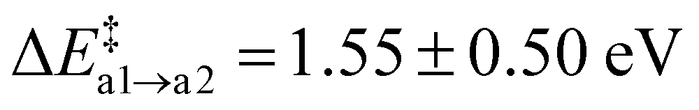 . The resulting Ni configuration is slightly favoured over the initial Oi configuration with a reaction energy ΔrEa2 = −0.7 ± 1.09 eV, yet the gain in energy is marginal. In contrast to that, the formation of an N2 dimer from Ni and a close by N from the amorphous network comes with a substantial barrier of
  because of the concerted breaking of four Si–N bonds. The resulting nitrogen vacancy in the final state also results in a high reaction energy (ΔrEa3 = 2.62 ± 1.54 eV), which is not compensated by the energy gained from the inherently stable N2 moiety. Compared to the transition state, the N–N bond shortens from 1.50 Å to 1.12 Å on average (Fig. 6a, 2 → 3), which is in good agreement with NN in the gas phase.101 Furthermore, the Mulliken charges on the N atoms are reduced to qmul = 0.02e. Both findings suggest that the N2 moiety does not interact with the a-Si3N4 surroundings, thus justifying calling it N2(g). The VN site undergoes geometric relaxation such that two vacant binding sites form an Si–Si bond with a length of ≈2.4 Å. However, this occurs to varying degrees due to the aforementioned rigidity of the amorphous network, causing a significant standard deviation for ΔrE. Formally, the N atoms are oxidised according to 2N3− → N02 so that six electrons have to be redistributed within a-Si3N4:O. The oxygen atom takes up two electrons according to O0i → ON2−, analogous to what has previously been observed for isolated ON defects. The four remaining electrons are distributed then over the VN site. There, they occupy the empty states of the emerging K-centres, which consequently relax to Si–Si dumbbell configurations as described by Gritsenko et al.,102 while the native electron traps remain unoccupied (see Fig. 6d). The average Si–Si bond length of these dumbbell configurations is 2.38 Å, which is similar to the values found for pure silicon (2.35 Å).101
With a second Oi atom present adjacent to the substitution site, N2(g) forms via a similar mechanism (path b). Starting from an Ni defect, the average barrier height  is similar to the corresponding one of path (a)
 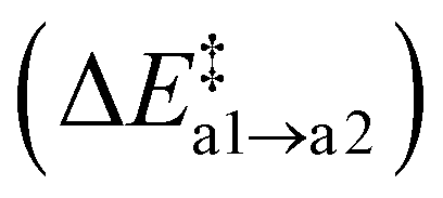 , confirming that this step is governed by the breaking of the Si–N bond. However, the resulting Ni configurations show a notable shift towards lower energies, i.e., ΔrEb2 = −1.22 ± 1.05 eV. Likewise, the barrier for the release of N2 is significantly reduced to
  . Both findings suggest that the nearby Oi atom helps to stabilise the system along the MEP by occupying the emerging nitrogen vacancy. This happens to varying degrees depending on how strongly the second Oi initially binds to a-Si3N4 and how much structural rearrangement is required, resulting in notable standard deviations for both ΔrEb2 and
  . In the most extreme case, the second O atom can already fully form the Si–O–Si configuration in the first step (see lowest energy path “outlier” in Fig. 6b coloured in gray). However, this remains an exception as it requires the amorphous network to spontaneously incorporate oxygen, which is rarely the case as discussed in Section 3.1. The final product state is again similar to that of path a with a N2(g) molecule in the local cavity. Not surprisingly, in all six cases, ΔrEb3 = −1.86 ± 0.45 eV is much lower compared to path (a), since the second Oi fills up the vacancy forming a second ON defect. This time, only two electrons have to be redistributed to the amorphous network as four are already taken up by the two ON atoms. Without VN, no Si–Si bonds are formed and the only potential recipients are the native traps or the new K-centre adjacent to ON. As already discussed in Section 3.2, it is solely their relative energetic level that determines which site is occupied, i.e., the DOS shown in Fig. 6e is characteristic for new K-centres forming a bipolaron while the native trap remains empty.
Path (b) requires the second Oi to be in the rear of the reaction site to occupy the emerging vacancy. If it is situated in the same cavity as the Ni defect, Oi can instead act as a scavenger for the N atom forming NO(g) (path c). This occurs in a single step without the formation of the Ni-intermediate. Both the average barrier height 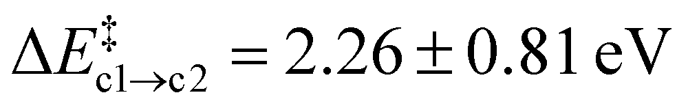 and the reaction energy ΔrEc2 = −0.89 ± 0.74 eV are rather modest.
  is similar to
 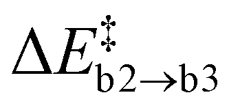 , suggesting that it is determined by the number of simultaneously broken Si–N bonds. The product state is approximately 1 eV higher in energy than the final state of path (b). This can be rationalised by N2(g) being thermodynamically favoured over NO(g) and only one of the two O atoms being bound in a favourable ON configuration. There is one outlier among the NO configurations (labelled as a hollow circle in Fig. 6c). It is caused by the geometric relaxation triggering the irreversible opening of strained rings in the vicinity of the reaction site. This leads to the formation of an Si–Si bond associated with
  . The electronic ground state of NO(g) is characterised by an unpaired electron and a small HOMO–LUMO gap, which can facilitate charge transfer to and from the molecule103–105 and could thus affect states at the VBM or CBM, respectively. Formally, the nitrogen atom is oxidised from N3− to N2+ in NO, thus one extra electron remains within a-Si3N4 (2O0 + 5e− → 2O2− + 1e−). The Mulliken charges of −0.16e and −0.01e on the O and N atom, respectively, suggest that this excess electron occupies the π*-orbital of the NO molecule. Energetically, the π* state lies 0.94 eV above the VBM of a-Si3N4, placing it between the hole and electron traps. As a result, the VBM and CBM remain unaffected (Fig. 6f), and the NO molecule continues to weakly interact with the positively polarised Si atoms in the amorphous network. Testing several configurations showed that there is little energetic difference between NO interacting with different nearby Si atoms. Hence, it is primarily a non-site-specific electrostatic interaction.
4 Discussion
We first return to the isolated oxygen defects and discuss their role in the electronic properties of a-Si3N4 in comparison to the most common crystalline phase of silicon nitride (β-Si3N4). We qualitatively confirm the findings by Grillo48 by repeating their calculations for ON defects in β-Si3N4 within our computational setup (see Section S3 in the SI): the excess electron localises on the emerging dangling Si-bond, forming a state within the band gap 2.97 eV above the valence band minimum. This state is the precursor for adding or removing electrons from the system, i.e., oxygen defects dictate charge trapping phenomena in β-Si3N4. For a-Si3N4 on the other hand, a different picture emerges. Here, the excess electron typically localises on the intrinsic trap, while the ON states are buried deep in the valence band. The instances in which the electron localises at the defect site occur solely when the newly formed dangling Si-bond is unable to be stabilised through coulombic interaction with the oxygen atom. This coincides with noticeable structural rearrangement of the amorphous network, i.e., the Si atom rearranges itself such that an electron can be trapped despite the vicinity of the highly negatively polarised O atom. Consequently, ON defects add K-centres to the already existing ones, and it is solely their relative energy levels in the band gap that determine where the trapping of electrons occurs. In both scenarios, the trapping remains governed by a dangling Si bond, while the oxygen states lie deep in the valence band and remain electronically idle. Hence, charge trapping remains a feature of the a-Si3N4 network topology and, in the dilute limit, is affected by oxygen only to the extent that it alters the local structure. Since such competition between trap sites and structural rearrangement are not possible in β-Si3N4, the defect site is the only precursor for charge trapping. The comparison to the amorphous phase suggests, that it is rather a feature of the point defect in the crystal lattice than of the oxygen itself. This interpretation also ties in with the observation by Bermudez,49 who reported electron trapping at the β-Si3N4 (0001) surface with subsurface ON defects. In this scenario, there is a surface state 2.5 eV above the VBM and therefore the surface provides a lower-lying trap state compared to the 1/3VN site.This phenomenon has also been observed for hydrogen and lithium defects:70,85,106 also these dopants primarily act as a source of electrons and inflict structural modification while not necessarily altering the mid-gap states. Thus charge trapping and charge transition levels remain dictated by pristine a-Si3N4. As long as dopants do not affect the electronic states near the band edges through structural modification, the dopant atom type does not play a role beyond being an electron donor or acceptor. In the context of application in memory devices, that means that in the dilute limit, the effect of oxygen defects on the properties of a-Si3N4 is limited, i.e., only a few outliers induce new mid-gap states, and a widening of the band gap is not observed in the concentrations considered here. However, this picture likely changes for higher defect concentrations, especially when the number of ON defects that create new trap sites increases, posing a worthwhile question for future research.
We now come back to the mechanism for the initial incorporation of oxygen into the amorphous network of a-Si3N4. Although Si–O bonds are energetically much more stable than Si–N bonds, the substitution does not occur in a straightforward fashion. Starting from Oi defects, there is a clear driving force to form Si–O–Si sites, but non-inserted Oi defects are energetically unfavourable. This phenomenon is attributed to the high density and rigidity of a-Si3N4 due to the threefold coordinated nitrogen atoms preventing the required structural relaxation. Likewise, replacing a nitrogen atom creates an interstitial that binds very strongly to the amorphous network. Ni diffusion rates are thus very likely too low at relevant temperatures, thus requiring the formation of gaseous molecular species (which are hardly bound to a-Si3N4) in additional steps. Among these, the direct formation of N2 is the least favourable due to the concomitant creation of a nitrogen vacancy, which comes at a notably higher barrier than alternative reaction pathways involving more than a single Oi (oxygen excess). However, a-Si3N4 is known as a material with very low oxygen diffusivity, which likely restricts the feasibility of those alternative pathways. Measured activation energies range from 3 eV to 5 eV,51,64,107i.e., they are higher than the barriers in the rate-controlling steps of the more favourable oxygen excess pathways. Still, without knowing inward diffusion barriers for Oi and outward diffusion barriers for gaseous products, this does not rule out any of the reaction pathways we have considered here. Mass spectrometry experiments found an NO2(g):NO(g) ratio of approximately 8:1 during oxidation of a-Si3N469—which cannot be explained by comparing the Gibbs free energy changes associated with the exclusive formation of either of these two products.108 Taking the decomposition 2NO → N2 + O2 at the elevated temperatures in these oxidation experiments into account, the amount of NO might even be underestimated by this ratio. This aligns well with the similar reaction energies and (rate-controlling) barriers in both of our oxygen excess pathways, where N2(g) or NO(g) are being formed.
Finally, we contextualise our findings within the Deal–Grove mechanism. It is reasonable to assume that at least at a gas–surface interface oxygen diffusion is not a limitation. If the amorphous network is not severely modified by the surface topology, our oxygen excess reaction pathways could thus rationalise the observed rapid onset of the oxidation. This would provide an atomic-scale indication why the Deal–Grove mechanism fails to describe this initial regime of the oxidation of a-Si3N4. That said, we emphasise that we cannot make any clear statements about the diffusion-limited regime at a later stage when a thick oxide layer has already been formed, but we note that the diffusion of gaseous reaction products has been discussed in previous work.62,64–66 Our findings tie into the mixed model proposed by Luthra,109 according to which the reaction is both controlled by diffusion and the interface reaction. If limited diffusion and the low permeability of a-Si3N4 do indeed prevent oxygen from accumulating at reaction sites as discussed above, the nitrogen vacancy pathway may well be unavoidable and hence not negligible for the macroscopic process. In that case, describing the effective oxidation rate would require a mixed model where the interface reaction and diffusion barriers are comparably large.
5 Conclusions
In summary, virtually all oxygen substitutional defects exhibit negative formation energies confirming a-Si3N4 predisposition towards oxidation. Even in the dilute limit of our samples, this has a marked impact on the electronic structure, as each oxygen substitution creates a dangling Si bond. The resulting K-centre remains positively charged and is stabilised by the nearby oxygen via Coulomb interaction. However, if further structural relaxation occurs and this stabilising effect is lost, the K-centre begins to compete with native electron traps present in pristine a-Si3N4. These traps are shallow in nature, thereby explaining the experimentally observed increase in charge carrier mobility in SiNxOy. Likewise, this suggests that the changes in material properties described in Section 1 are primarily caused by structural modifications and local stoichiometric imbalance, not directly by the electronic levels of oxygen.Spontaneous oxygen incorporation, however, is observed only in rare cases where two Si atoms with pre-strained Si–N bonds are already aligned, enabling direct oxygen insertion. These interstitials partially insert into Si–N bonds and eventually form Si–O–Si bridges, resembling a silica-like structure. However, substituted nitrogen atoms remain bound to the amorphous network as nitrogen interstitials, which cannot easily diffuse away from the reaction site and needs to be transformed into a gaseous molecule. Forming N2(g) comes with a formidable energetic barrier associated with the concerted breaking of several Si–N bonds and energetically unfavourable product states owing the formation of nitrogen vacancies. Alternative routes via the concerted substitution of two nitrogen atoms lower the barriers and the energy of the product states considerably. In the process the VN is avoided, resulting in either N2(g) or NO(g) by intercepting the emerging Ni. This rationalises the formidable oxidation resistance of a-Si3N4 as well as the experimentally detected NO2(g):NO(g) ratio with an unexpectedly high abundance of NO(g).
Author contributions
LH: conceptualization, data curation, formal analysis, investigation, methodology, software, validation, visualisation, writing – original draft. RS: investigation. FB: investigation. JC: conceptualization, project administration, supervision, validation, writing – review & editing. JM: conceptualization, funding acquisition, resources, supervision, validation, writing – review & editing.Conflicts of interest
There are no conflicts to declare.Data availability
All structures generated in this study are available via zenodo.org at https://doi.org/10.5281/zenodo.15206130, together with input parameters and specifications for the compilation of the CP2K package.Supplementary information (SI): ensemble subset selection for HSE06 calculations; additional characterisation of defects; oxygen defects in crystalline silicon nitride. See DOI: https://doi.org/10.1039/d5tc03484a.
Acknowledgements
This research is co-financed by Holland High Tech through a public–private partnership in research and development within the Dutch top sector of High-Tech Systems and Materials (HTSM). The use of the national computer facilities in this research was subsidised by NWO Domain Science (grant no. 2024.029) and supported by the SURF Cooperative (grant no. EINF-6913 and EINF-9872).References
- M. Vila, D. Cáceres and C. Prieto, J. Appl. Phys., 2003, 94, 7868 CrossRef CAS.
- X. Dong, J. Wu, H. Yu, Q. Zhou, W. Wang, X. Zhang, L. Zhang, L. Li and R. He, Int. J. Appl. Ceram. Technol., 2022, 19, 2929–2949 CrossRef CAS.
- J. Barta, M. Manela and R. Fischer, Mater. Sci. Eng., 1985, 71, 265–272 CrossRef CAS.
- J. V. Dalton and J. Drobek, J. Electrochem. Soc., 1968, 115, 865 CrossRef CAS.
- F. L. Riley, J. Am. Ceram. Soc., 2000, 83, 245–265 CrossRef CAS.
- X. Li, X. Yin, L. Zhang, L. Cheng and Y. Qi, Mater. Sci. Eng., A, 2009, 500, 63–69 CrossRef.
- H. Du, Y. Li and C. Cao, J. Alloys Compd., 2010, 503, L9–L13 CrossRef CAS.
- J. Resende, D. Fuard, D. Le Cunff, J.-H. Tortai and B. Pelissier, Mater. Chem. Phys., 2021, 259, 124000 CrossRef CAS.
- S. M. Hu, D. R. Kerr and L. V. Gregor, Appl. Phys. Lett., 1967, 10, 97–99 CrossRef CAS.
- T. L. Chu, J. R. Szedon and C. H. Lee, Solid-State Electron., 1967, 10, 897–905 CrossRef CAS.
- H.-W. Liu, H.-P. Su, W.-K. Lai and H.-C. Cheng, J. Electrochem. Soc., 1997, 144, 3288 CrossRef CAS.
- S. J. Wrazien, Y. Zhao, J. D. Krayer and M. H. White, Solid-State Electron., 2003, 47, 885–891 CrossRef CAS.
- J. S. Meena, S. M. Sze, U. Chand and T.-Y. Tseng, Nanoscale Res. Lett., 2014, 9, 526 CrossRef.
- L. Wang, C.-H. Yang and J. Wen, Electron. Mater. Lett., 2015, 11, 505–543 CrossRef CAS.
- K.-R. Nam, J.-k Jeong, J.-Y. Sung and G.-W. Lee, Trans. Electr. Electron. Mater., 2021, 22, 372–377 CrossRef.
- J. Robertson and M. J. Powell, Appl. Phys. Lett., 1984, 44, 415–417 CrossRef CAS.
- W. L. Warren, P. M. Lenahan and S. E. Curry, Phys. Rev. Lett., 1990, 65, 207–210 CrossRef CAS PubMed.
- J. Robertson, Philos. Mag., B, 1991, 63, 47–77 CAS.
- W. L. Warren, J. Kanicki, J. Robertson, E. H. Poindexter and P. J. McWhorter, J. Appl. Phys., 1993, 74, 4034–4046 CrossRef CAS.
- D. T. Krick, P. M. Lenahan and J. Kanicki, J. Appl. Phys., 1988, 64, 3558–3563 CrossRef CAS.
- E. Vianello, L. Perniola, P. Blaise, G. Molas, J. P. Colonna, F. Driussi, P. Palestri, D. Esseni, L. Selmi, N. Rochat, C. Licitra, D. Lafond, R. Kies, G. Reimbold, B. de Salvo and F. Boulanger, 2009 IEEE International Electron Devices Meeting (IEDM), 2009, pp. 1–4.
- C. Di Valentin, G. Palma and G. Pacchioni, J. Phys. Chem. C, 2011, 115, 561–569 CrossRef CAS.
- G. Kang, D. Lee, K. Lee, J. Kim and S. Han, Phys. Rev. Appl., 2018, 10, 064052 CrossRef CAS.
- C. Wilhelmer, D. Waldhoer, L. Cvitkovich, D. Milardovich, M. Waltl and T. Grasser, Nanomaterials, 2023, 13, 2286 CrossRef CAS.
- W. I. Choi, W.-J. Son, R. Dronskowski, Y. Oh, S.-Y. Yang, U. Kwon and D. S. Kim, Adv. Mater., 2024, 36, 2308054 CrossRef CAS.
- M. Boero, K. Shiraishi, T. Nagahashi, F. Nanataki and A. Oshiyama, Phys. Rev. Mater., 2025, 9, 084601 CrossRef CAS.
- M. Herrmann and A. Schenk, J. Appl. Phys., 1995, 77, 4522–4540 CrossRef CAS.
- A. Arreghini, F. Driussi, E. Vianello, D. Esseni, M. J. van Duuren, D. S. Golubovic, N. Akil and R. van Schaijk, IEEE Trans. Electron Devices, 2008, 55, 1211–1219 CAS.
- C.-Y. Lu, J. Nanosci. Nanotechnol., 2012, 12, 7604–7618 CrossRef CAS PubMed.
- S. Choi, Y. Lim, S. Kim, S. Park, B. Ku, H. Kim, J. Yang, B. Kim, Y. Son, H. Choi and C. Choi, Adv. Electron. Mater., 2025, 11, e00960 CrossRef CAS.
- I. Lee, J. W. Na, K. Kwak, J. B. An and H. J. Kim, Appl. Surf. Sci. Adv., 2025, 29, 100839 CrossRef.
- T. V. Perevalov, V. A. Volodin, G. N. Kamaev, A. A. Gismatulin, S. G. Cherkova, I. P. Prosvirin, K. N. Astankova and V. A. Gritsenko, J. Non-Cryst. Solids, 2022, 598, 121925 CrossRef CAS.
- Y. N. Novikov, G. N. Kamaev, I. P. Prosvirin and V. A. Gritsenko, Appl. Phys. Lett., 2023, 122, 232903 CrossRef CAS.
- K. Ermak, G. Kamaev and V. Volodin, 2025 IEEE 26th International Conference of Young Professionals in Electron Devices and Materials (EDM), 2025, pp. 70–73.
- V. J. Kapoor, R. S. Bailey and S. R. Smith, J. Vac. Sci. Technol., 1981, 18, 305–308 CrossRef CAS.
- D. Xu and V. J. Kapoor, J. Appl. Phys., 1991, 70, 1570–1574 CrossRef CAS.
- J.-l Yeh and S.-C. Lee, J. Appl. Phys., 1996, 79, 656–663 CrossRef CAS.
- V. A. Gritsenko, H. Wong, J. B. Xu, R. M. Kwok, I. P. Petrenko, B. A. Zaitsev, Y. N. Morokov and Y. N. Novikov, J. Appl. Phys., 1999, 86, 3234–3240 CrossRef CAS.
- P. Karakolis, P. Normand, P. Dimitrakis, L. Sygelou, V. Ntinas, I. A. Fyrigos, I. Karafyllidis and G. C. Sirakoulis, 2019 IEEE/ACM International Symposium on Nanoscale Architectures (NANOARCH), 2019, pp. 1–2.
- N. Vasileiadis, P. Karakolis, P. Mandylas, V. Ioannou-Sougleridis, P. Normand, M. Perego, P. Komninou, V. Ntinas, I.-A. Fyrigos, I. Karafyllidis, G. C. Sirakoulis and P. Dimitrakis, IEEE Trans. Nanotechnol., 2021, 20, 356–364 CAS.
- C.-M. Mo, L. Zhang, C. Xie and T. Wang, J. Appl. Phys., 1993, 73, 5185–5188 CrossRef CAS.
- Y. Liu, Y. Zhou, W. Shi, L. Zhao, B. Sun and T. Ye, Mater. Lett., 2004, 58, 2397–2400 CrossRef CAS.
- P. D. Nguyen, D. M. Kepaptsoglou, Q. M. Ramasse, M. F. Sunding, L. O. Vestland, T. G. Finstad and A. Olsen, J. Appl. Phys., 2012, 112, 073514 CrossRef.
- J.-Y. Sung, J.-k Jeong, K.-R. Nam and G.-W. Lee, Trans. Electr. Electron. Mater., 2021, 22, 432–438 CrossRef.
- C. Sandhya, A. B. Oak, N. Chattar, A. S. Joshi, U. Ganguly, C. Olsen, S. M. Seutter, L. Date, R. Hung, J. Vasi and S. Mahapatra, IEEE Trans. Electron Devices, 2009, 56, 3123–3132 CAS.
- J. H. You, H. W. Kim, D. H. Kim, T. W. Kim and K. W. Lee, 2011 International Conference on Simulation of Semiconductor Processes and Devices, 2011, pp. 199–202.
- D. Chen, S. Huang and L. He, J. Semicond., 2017, 38, 043002 CrossRef.
- M. E. Grillo, S. D. Elliott, J. Rodríguez, R. Añez, D. S. Coll, A. Suhane, L. Breuil, A. Arreghini, R. Degraeve, A. Shariq, V. Beyer and M. Czernohorsky, Comput. Mater. Sci., 2014, 81, 178–183 CrossRef CAS.
- V. M. Bermudez, Surf. Sci., 2020, 691, 121511 CrossRef CAS.
- L. Hückmann, J. Cottom and J. Meyer, Adv. Phys. Res., 2024, 3, 2300109 CrossRef.
- W. C. Tripp and H. C. Graham, J. Am. Ceram. Soc., 1976, 59, 399–403 CrossRef CAS.
- F. Porz and F. Thmmler, J. Mater. Sci., 1984, 19, 1283–1295 CrossRef CAS.
- I. I. López-López, A. Contreras, R. Morales-Estrella and J. Lemus-Ruiz, Silicon, 2023, 15, 3181–3192 CrossRef.
- S. I. Raider, R. Flitsch, J. A. Aboaf and W. A. Pliskin, J. Electrochem. Soc., 1976, 123, 560–565 CrossRef CAS.
- N. Banerji, J. Serra, P. González, S. Chiussi, E. Parada, B. León and M. Pérez-Amor, Thin Solid Films, 1998, 317, 214–218 CrossRef CAS.
- W.-S. Liao, C.-H. Lin and S.-C. Lee, Appl. Phys. Lett., 1994, 65, 2229–2231 CrossRef CAS.
- D. Z. Gao, A.-M. El-Sayed and A. L. Shluger, Nanotechnology, 2016, 27, 505207 CrossRef PubMed.
- K. Kakishita, A. Otani, E. Ohta and M. Sakata, Jpn. J. Appl. Phys., 1989, 28, 1147 CrossRef CAS.
- L. U. T. Ogbuji and D. T. Jayne, J. Electrochem. Soc., 1993, 140, 759–766 CrossRef CAS.
- M. Lisiansky, A. Heiman, M. Kovler, A. Fenigstein, Y. Roizin, I. Levin, A. Gladkikh, M. Oksman, R. Edrei, A. Hoffman, Y. Shnieder and T. Claasen, Appl. Phys. Lett., 2006, 89, 153506 CrossRef.
- M. Chang, Y. Ju, J. Lee, S. Jung, H. Choi, M. Jo, S. Jeon and H. Hwang, Appl. Phys. Lett., 2008, 93, 022101 CrossRef.
- A. E. T. Kuiper, M. F. C. Willemsen, J. M. L. Mulder, J. B. O. Elferink, F. H. P. M. Habraken and W. F. van der Weg, J. Vac. Sci. Technol., B, 1989, 7, 455–465 CrossRef CAS.
- B. E. Deal and A. S. Grove, J. Appl. Phys., 1965, 36, 3770–3778 CrossRef CAS.
- H. Du, R. E. Tressler, K. E. Spear and C. G. Pantano, J. Electrochem. Soc., 1989, 136, 1527–1536 CrossRef CAS.
- A. Kuiper, M. Willemsen, J. Bax and F. Habraken, Appl. Surf. Sci., 1988, 33–34, 757–764 CrossRef.
- F. Habraken and A. Kuiper, Mater. Sci. Eng., R, 1994, 12, 123–175 CrossRef.
- D. P. Butt, D. Albert and T. N. Taylor, J. Am. Ceram. Soc., 1996, 79, 2809–2814 CrossRef CAS.
- L. U. J. T. Ogbuji, J. Am. Ceram. Soc., 1995, 78, 1279–1284 CrossRef CAS.
- R. Wang, C. Zhang, D. Li, Z. Xie, Y. Zhang and X. Lu, Ceram. Int., 2021, 47, 33078–33088 CrossRef CAS.
- J. Cottom, L. Hückmann, E. Olsson and J. Meyer, J. Phys. Chem. Lett., 2024, 15, 840–848 CrossRef CAS PubMed.
- T. D. Kühne, M. Iannuzzi, M. Del Ben, V. V. Rybkin, P. Seewald, F. Stein, T. Laino, R. Z. Khaliullin, O. Schütt, F. Schiffmann, D. Golze, J. Wilhelm, S. Chulkov, M. H. Bani-Hashemian, V. Weber, U. Borštnik, M. Taillefumier, A. S. Jakobovits, A. Lazzaro, H. Pabst, T. Müller, R. Schade, M. Guidon, S. Andermatt, N. Holmberg, G. K. Schenter, A. Hehn, A. Bussy, F. Belleflamme, G. Tabacchi, A. Glöβ, M. Lass, I. Bethune, C. J. Mundy, C. Plessl, M. Watkins, J. VandeVondele, M. Krack and J. Hutter, J. Chem. Phys., 2020, 152, 194103 CrossRef PubMed.
- J. van de Vondele and J. Hutter, J. Chem. Phys., 2007, 127, 114105 CrossRef.
- S. Goedecker, M. Teter and J. Hutter, Phys. Rev. B: Condens. Matter Mater. Phys., 1996, 54, 1703–1710 CrossRef CAS PubMed.
- C. Hartwigsen, S. Goedecker and J. Hutter, Phys. Rev. B: Condens. Matter Mater. Phys., 1998, 58, 3641–3662 CrossRef CAS.
- C. G. Broyden, IMA J. Appl. Math., 1970, 6, 222–231 CrossRef.
- R. Fletcher, Comput. J., 1970, 13, 317–322 CrossRef.
- D. Goldfarb, Math. Comput., 1970, 24, 23–26 CrossRef.
- D. F. Shanno, Math. Comput., 1970, 24, 647–656 CrossRef.
- J. P. Perdew, K. Burke and M. Ernzerhof, Phys. Rev. Lett., 1996, 77, 3865–3868 CrossRef CAS PubMed.
- J. P. Perdew, K. Burke and M. Ernzerhof, Phys. Rev. Lett., 1997, 78, 1396 CrossRef CAS.
- J. Heyd, G. E. Scuseria and M. Ernzerhof, J. Chem. Phys., 2003, 118, 8207–8215 CrossRef CAS.
- J. Heyd, G. E. Scuseria and M. Ernzerhof, J. Chem. Phys., 2006, 124, 219906 CrossRef.
- R. S. Mulliken, J. Chem. Phys., 1955, 23, 1833–1840 CrossRef CAS.
- C. M. Marian, M. Gastreich and J. D. Gale, Phys. Rev. B: Condens. Matter Mater. Phys., 2000, 62, 3117–3124 CrossRef CAS.
- J. Cottom, L. Hückmann, J. Meyer and E. Olsson, J. Mater. Chem. A, 2025, 13, 34260–34272 RSC.
- L. Hückmann, J. Cottom and J. Meyer, Intrinsic Charge Trapping and Reversible Charge Induced Structural Modifications in a-Si3N4, 2023 DOI:10.5281/zenodo.8239086.
- S. B. Zhang and J. E. Northrup, Phys. Rev. Lett., 1991, 67, 2339–2342 CrossRef CAS.
- W. H. Baur, Z. Kristallogr. - Cryst. Mater., 2009, 224, 580–592 CrossRef CAS.
- D. du Boulay, N. Ishizawa, T. Atake, V. Streltsov, K. Furuya and F. Munakata, Acta Crystallogr., Sect. B, 2004, 60, 388–405 CrossRef CAS PubMed.
- H. Jónsson, G. Mills and K. W. Jacobson, Classical and Quantum Dynamics in Condensed Phase Simulations, 1998, pp. 385–404 Search PubMed.
- G. Henkelman, B. P. Uberuaga and H. Jónsson, J. Chem. Phys., 2000, 113, 9901–9904 CrossRef CAS.
- G. Henkelman and H. Jónsson, J. Chem. Phys., 2000, 113, 9978–9985 CrossRef CAS.
- K. Kajihara, T. Miura, H. Kamioka, A. Aiba, M. Uramoto, Y. Morimoto, M. Hirano, L. Skuja and H. Hosono, J. Non-Cryst. Solids, 2008, 354, 224–232 CrossRef CAS.
- W. J. Malfait, W. E. Halter and R. Verel, Chem. Geol., 2008, 256, 269–277 CrossRef CAS.
- V. A. Gritsenko, S. S. Nekrashevich, V. V. Vasilev and A. V. Shaposhnikov, Microelectron. Eng., 2009, 86, 1866–1869 CrossRef CAS.
- R. D. Harcourt, J. Mol. Struct., 1990, 206, 253–264 CrossRef.
- A. F. Young, J. A. Montoya, C. Sanloup, M. Lazzeri, E. Gregoryanz and S. Scandolo, Phys. Rev. B: Condens. Matter Mater. Phys., 2006, 73, 153102 CrossRef.
- K. Niwa, T. Yamamoto, T. Sasaki and M. Hasegawa, Phys. Rev. Mater., 2019, 3, 053601 CrossRef CAS.
- B. Bhattacharjee and E. Olsson, Phys. Chem. Chem. Phys., 2025, 27, 22610–22620 RSC.
- J. Paier, R. Hirschl, M. Marsman and G. Kresse, J. Chem. Phys., 2005, 122, 234102 CrossRef PubMed.
- E. Wiberg, N. Wiberg and A. F. Holleman, Anorganische Chemie, De Gruyter, Berlin and Boston, 103rd edn, 2017 Search PubMed.
- V. A. Gritsenko, T. V. Perevalov, O. M. Orlov and G. Y. Krasnikov, Appl. Phys. Lett., 2016, 109, 062904 CrossRef.
- W. Kaim, Angew. Chem., Int. Ed., 2011, 50, 10498–10500 CrossRef CAS PubMed.
- J. E. M. N. Klein, B. Miehlich, M. S. Holzwarth, M. Bauer, M. Milek, M. M. Khusniyarov, G. Knizia, H.-J. Werner and B. Plietker, Angew. Chem. Int. Ed., 2014, 53, 1790–1794 CrossRef CAS PubMed.
- W. Kaim, A. Das, J. Fiedler, S. Záliš and B. Sarkar, Coord. Chem. Rev., 2020, 404, 213114 CrossRef CAS.
- C. Wilhelmer, D. Waldhör, L. Cvitkovich, D. Milardovich, M. Waltl and T. Grasser, Phys. Rev. B, 2024, 110, 045201 CrossRef CAS.
- T. Hirai, K. Niihara and T. Goto, J. Am. Ceram. Soc., 1980, 63, 419–424 CrossRef CAS.
- M. A. Frisch and J. L. Margrave, J. Phys. Chem., 1965, 69, 3863–3866 CrossRef CAS.
- K. L. Luthra, J. Electrochem. Soc., 1991, 138, 3001 CrossRef CAS.
| This journal is © The Royal Society of Chemistry 2026 |