
 Open Access Article
 This Open Access Article is licensed under a Creative Commons Attribution-Non Commercial 3.0 Unported Licence
Preferentially oriented SrTiO3 thin films grown on lanthanide-assisted Si(001) via pulsed laser deposition
Hannes
Rijckaert†
 *a,
Giovanna
Latronico†
b,
Davy
Deduytsche‡
c,
Eduardo
Solano
d,
Petriina
Paturi
e and
Paolo
Mele
f
*a,
Giovanna
Latronico†
b,
Davy
Deduytsche‡
c,
Eduardo
Solano
d,
Petriina
Paturi
e and
Paolo
Mele
f
aSCRiPTS, Department of Chemistry, Ghent University, Krijgslaan 281-S3, 9000 Ghent, Belgium. E-mail: Hannes.Rijckaert@UGent.be
bShibaura Research Laboratories, Shibaura Institute of Technology, Omiya Campus, 307 Fukasaku, Minuma-ku, Saitama City, Saitama 337-8570, Japan
cCoCooN Group, Department of Solid State Sciences, Ghent University, Krijgslaan 281-S1, 9000 Ghent, Belgium
dNCD-SWEET beamline, ALBA Synchrotron Light Source, Carrer de la Llum 2-26, 08290 Cerdanyola del Vallès, Spain
eWihuri Physical Laboratory, Department of Physics and Astronomy, University of Turku, Vesilinnantie 5, 20014, Turku, Finland
fCollege of Engineering, Shibaura Institute of Technology, Omiya Campus, 307 Fukasaku, Minuma-ku, Saitama City, Saitama 337-8570, Japan
First published on 10th December 2025
Abstract
The integration of high-quality SrTiO3 thin films on silicon substrates is crucial for various applications. This work investigates the use of an out-of-plane, self-oriented La2O2CO3 seed layer prepared via the chemical solution deposition (CSD) method as a template for SrTiO3 growth by pulsed laser deposition (PLD). The growth window of the SrTiO3 thin film was determined by in situ X-ray diffraction and by studying the thermal stability of the La2O2CO3 film. This study resulted in crack-free films with preferential but not exclusive (001) out-of-plane orientation when using one-step PLD deposition at 750 °C. Further in-depth X-ray diffraction analysis revealed that the SrTiO3 film exhibited multiple preferential orientations rather than a continuous fibre texture. Transmission electron microscopy confirmed a uniform SrTiO3 film without interfacial reactions and a homogeneous composition. These findings highlight the key role of deposition conditions in controlling crystallinity and orientation, enabling the integration of high-quality perovskite oxide on silicon.
Introduction
Recently, strontium titanate (SrTiO3) thin films have emerged as a promising lead-free material due to their functional and practical advantages. In terms of functional properties, SrTiO3 exhibits a large dielectric constant, high breakdown strength, and tunable electrical conductivity via doping. These properties make it attractive for applications in energy storage and non-volatile memory devices.1,2 Additionally, SrTiO3 is identified as an ideal candidate for cryogenic applications due to its low Curie temperature, enabling the exploration of piezo-electric and electro-optic effects at cryogenic temperatures.3 Room-temperature ferroelectric properties, such as the electrocaloric effect, have also been reported when epitaxial strain is achieved via strain engineering due to the lattice mismatch with appropriate substrates.4,5In fact, beyond their potential use with functionality in several applications, these SrTiO3 thin films can serve effectively as buffer template layers for the monolithic integration of Ge, III–V heterostructures, or other perovskite oxide materials such as BaTiO3, SrRuO3 and Pb(Zr, Ti)O3 (PZT) on Si(001) wafers.6–8 Therefore, the direct heteroepitaxy of SrTiO3 on Si wafers is an important step toward enabling the integration of multifunctional perovskite oxides onto large-scale wafers. Several deposition techniques have been introduced to grow SrTiO3 thin films as a buffer layer on Si wafers, with molecular-beam epitaxy (MBE) and pulsed laser deposition (PLD) being two of the most commonly used methods.9
MBE is suitable for epitaxial growth due to its slow growth rate and precise control of atomic growth. However, the low oxygen partial pressure, typically limited to a maximum of 10−5 mbar, promotes the formation of oxygen vacancies in the SrTiO3 thin film, which significantly influences functional properties.10 To eliminate these oxygen vacancies, post-annealing at high temperatures, especially under high oxygen pressure, is introduced, resulting in generally strong interfacial reactions with Si substrates.10 Compared to the MBE technique, PLD can reach a higher oxygen pressure of above 10−2 mbar and offers better control over oxygen vacancies. Nevertheless, the direct epitaxy of oxides on the Si wafer by PLD is still a challenge due to the higher O2 pressure, which results in amorphous SiO2 interface formation and a lack of atomic control. This shows the difficulty of growing various multifunctional perovskite oxide materials on Si wafers due to the presence of the interfacial SiO2 layer, which prevents direct oriented growth. Prior to the direct deposition onto Si wafers, this interfacial oxide needs to be properly addressed.
Several approaches reported in the literature have been proposed to overcome this issue. A commonly used method involves introducing a SrO buffer layer,11 although this often leads to SrTiO3 thin-film growth in the (110) orientation, which may not be desirable for all applications. Another strategy is the thermal treatment of the Si wafer by heating it to approximately 980 °C in an ultra-high vacuum to remove the native oxide.12–14 Alternatively, chemical etching with a 1% HF solution can be used to produce a hydrogen-terminated Si surface,11 which is preferred for pure oxide growth. A two-step deposition method has also been reported, where a thin SrTiO3 layer is first deposited at low temperature between 150 and 300 °C in a vacuum to initiate nucleation, followed by a final deposition step at 650 °C to enhance crystallinity and film quality.11,15 The group at the University of Twente16,17 has introduced inorganic 2D Ca2Nb3O10 nanosheets as a growth template layer on the Si wafer to grow artificial heteroepitaxial SrTiO3 thin films with (001) orientation.
Building on all these methods and addressing the challenges of large-area, wafer-scale deposition with high-throughput via PLD and MBE,18 we present a promising, high-throughput chemical solution deposition (CSD) process that uses a self-oriented La2O2CO3 template film, based on the work of Picavet et al.,19 to grow well-oriented SrTiO3 thin films on Si wafers using the PLD technique. The resulting highly textured film exhibits a preferential out-of-plane orientation and can serve as an integration tool for the growth of multifunctional perovskite oxide materials on Si-based platforms where full epitaxy is not required. Thus, the key factor is achieving a crystalline, textured, and preferentially oriented film that exhibits the desired ferroelectric and dielectric properties.
Experimental section
STO thin films were deposited on both La2O2CO3-templated and pristine Si(001) substrates using PLD. The Si substrates were cleaned by ultrasonic treatment in isopropanol (Kanto Chemical, >99.7%) for 5 minutes, followed by heating on a hotplate at 150 °C under ambient conditions to remove any solvent residues. The formulation of the precursor solution and the CSD method for growing the La2O2CO3 template film have been reported in previous works.19,20 A polyvinylpyrrolidone (PVP)-based solution was prepared by dissolving 0.05 g of a 40 wt% PVP solution (Alfa Aesar, 8000 g mol−1) in H2O into 40 mL of n-propanol (Chem-Lab, 99.8+%). The La2O2CO3 solution was prepared by dissolving La(NO3)3·6H2O (Merck, ≥99.99%) in n-propanol with a concentration of 0.06 mol L−1. The PVP solution was spin-coated onto treated 10 × 10 mm2 Si substrates at a spin rate of 2600 rpm for 30 seconds using the Kyowariken K-359S1 spin coater to enhance the wetting behavior at the surface interface. Directly after this spin-coating, the La2O2CO3 solution was spin-coated onto the PVP-modified Si substrate using the same spin-coating parameters. Subsequently, the coated substrates underwent a pyrolysis step at 200 °C for 5 minutes in ambient air, followed by an annealing step in dry static air with a heating rate of 12.5 °C min−1 to a final temperature of 485 °C, and were held for a dwelling time of 20 minutes. A stoichiometric SrTiO3 target (Toshima, purity 99.99%) was used for PLD growth with a Nd:YAG laser (YG-PLAD-241, LOTIS-TII, Minsk, Belarus) at a wavelength of 266 nm (fourth harmonic). The optimized laser parameters for high-quality SrTiO3 thin films were a repetition rate of 10 Hz and a laser fluence of 4 J cm−2. The distance between the target and the substrate was maintained at 35 mm.For determining deposition and growth windows, thermogravimetric analysis (TGA) and differential thermal analysis (DTA) were used with a NETZSCH (Selb, Germany) Model STA 449F3 Jupiter system at a heating rate of 10 °C min−1 under air atmosphere to understand the thermal decomposition of the La2O2CO3 precursor as a function of temperature. In situ X-ray diffraction (XRD) scans were carried out on a Bruker D8 Discover diffractometer equipped with a home-built annealing chamber (Ghent University) and a linear detector. Cu Kα radiation (λ = 1.5406 Å) was employed, and the sample was annealed in ambient air at a heating rate of 5 °C min−1 up to 750 °C, with data collected in the 2θ range of 20° to 50° and an integration time of 15 s. Before and after the annealing, ex situ XRD scans from 15° to 60° with a step size of 0.05° and an integration time of 1 s were taken. Atomic force microscopy measurements was carried out using a Bruker ICON Dimension microscope operated on tapping mode in air with Bruker TESPA-V2 cantilevers.
All the thin films were analyzed via ex situ XRD after the PLD depositions. Data acquisition was performed using a Bragg–Brentano powder diffractometer (Smart Lab Rigaku Corporation, Japan) with Cu Kα radiation (λ = 1.5406 Å) over an angular range of 15°-55° with an angular step of 0.01° (power settings: 50 mA, 40 kV). The grazing-incidence wide-angle X-ray scattering (GIWAXS) data were collected at the NCD-SWEET beamline of the ALBA Synchrotron Radiation Facility (Spain). The incident X-ray beam energy was set to 12.4 keV (λ = 0.9998 Å) using a channel-cut Si(111) monochromator. A stack of Be compound refractive lenses was employed to collimate the beam, resulting in a beam size of 50 × 150 µm2 (V × H) at the sample position. The angle of incidence (αi) was screened between 0° and 1°, and finally set to 0.325° to ensure surface sensitivity. An exposure time of 10 s was used. The scattering patterns were recorded using a Rayonix LX255-HS area detector, which consists of 1920 × 5760 pixels (H × V) with a pixel size of 44.27 × 44.27 µm2. The scattering vector q was calibrated using Cr2O3 as a standard, resulting in a sample-to-detector distance of 201.65 mm. The pole figures were measured using a Panalytical Empyrean diffractometer with a 5-axis goniometer, a Bragg-BrentanoHD collimator and a PIXCel3D detector using Cu Kα radiation. The pole figures were measured at constant 2θ/ω angles by varying the tilt angle (χ) and rotation angle (ϕ) and using the receiving slit mode with 0.25° width.
The topographical properties were characterized using scanning electron microscopy (SEM) with an FEI Nova 600 Nanolab Dual Beam system. Transmission electron microscopy (TEM) was used to study the microstructural properties of SrTiO3 films with a bright field (BF) detector and operated at a JEOL JEM-2200FS of the UGent TEM core facility with a working voltage of 200 kV. The composition was determined via energy-dispersive X-ray (EDX) spectroscopy and high-angle annular dark-field (HAADF) imaging in scanning TEM (STEM). For TEM investigations, a cross-sectional lamella was prepared by focused ion beam, utilizing an FEI Nova 600 dual beam system, following the procedure described in this technical note.21
Results and discussion
The out-of-plane self-oriented La2O2CO3 seed layer has been extensively described in the work of Picavet et al.,19 demonstrating its potential as a general integration tool for various ferroelectric films deposited via the CSD approach. This La2O2CO3 film exhibits a monoclinic structure (Type 1a) and has an in-plane lattice spacing (a) of 4.076 Å. Seed layers are required to act as a texture template for growth; their effectiveness is limited by the lattice spacing and the occupation of sites within the crystal lattice. Therefore, the lattice mismatch between the seed and the functional layer should be minimized as much as possible to grow a high-quality layer. Cubic SrTiO3 (space group: Pm![[3 with combining macron]](https://www.rsc.org/images/entities/char_0033_0304.gif) m, 221, PDF: 00-035-0734), with a bulk in-plane lattice spacing (a) of 3.905 Å, results in a theoretical tensile lattice mismatch of +4.2%, indicating the possibility of forming a tensile-strained SrTiO3 film. Therefore, La2O2CO3 film appears to be a promising candidate for growing SrTiO3 film. However, further investigation is required to evaluate the growth windows of La2O2CO3 and SrTiO3 films.
m, 221, PDF: 00-035-0734), with a bulk in-plane lattice spacing (a) of 3.905 Å, results in a theoretical tensile lattice mismatch of +4.2%, indicating the possibility of forming a tensile-strained SrTiO3 film. Therefore, La2O2CO3 film appears to be a promising candidate for growing SrTiO3 film. However, further investigation is required to evaluate the growth windows of La2O2CO3 and SrTiO3 films.
Each material system has its own growth windows, which define the limited range of thin film deposition. Since the thermal decomposition of the metal–organic precursor is one of the critical steps in CSD-based thin-film growth, TGA and DTA were introduced to provide detailed insights into the temperature dependence of the decomposition of La2O2CO3 solution (Fig. 1). The TGA curve shows three different mass loss stages in the temperature ranges of 100–260 °C, 260–450 °C, and 700–800 °C. In the first stage, the initial melting and dehydration, together with solvent evaporation, start around 100 °C with a mass loss of 25%. In the second stage, mass loss starts around 260 °C and is attributed to nitrate-containing compounds.22 This leads to a 35% weight reduction and a strong exothermic effect at 398 °C, as shown in the DTA curve (Fig. 1A, dashed line). After 450 °C, the La2O2CO3 phase remains stable (orange marking in Fig. 1A), and CO2 begins to release at 700 °C, causing a 5% mass loss. This leads to a phase transformation to La2O3, confirmed by an endothermic effect at 803 °C in the DTA curve. The formation of La2O3 phase is undesirable, as it can crystalize in two phases:23,24 cubic-La2O3 and hexagonal-La2O3, which can exhibit a large mismatch with the SrTiO3 thin film. La2O2CO3 films, prepared by the CSD method, require loading into the PLD chamber and heating to a specified substrate temperature prior to SrTiO3 deposition. Therefore, their thermal stability under vacuum conditions was evaluated. As-grown La2O2CO3 films were heated to 800 °C and held for 30 minutes in the PLD chamber under vacuum, followed by XRD analysis. The XRD patterns in Fig. 1B reveal a slight reduction in crystallinity, evidenced by peak broadening and a decrease in intensity. No formation of La2O3 phase peaks was observed, indicating phase stability under these conditions. However, the surface roughness for the as-grown La2O2CO3 films increases slightly after heating to 800 °C (RMS = 2.01) compared to the unheated films (RSM = 1.13). Therefore, when using the La2O2CO3 films as a seed layer for PLD deposition, exposure to high temperatures should be minimized as much as possible.
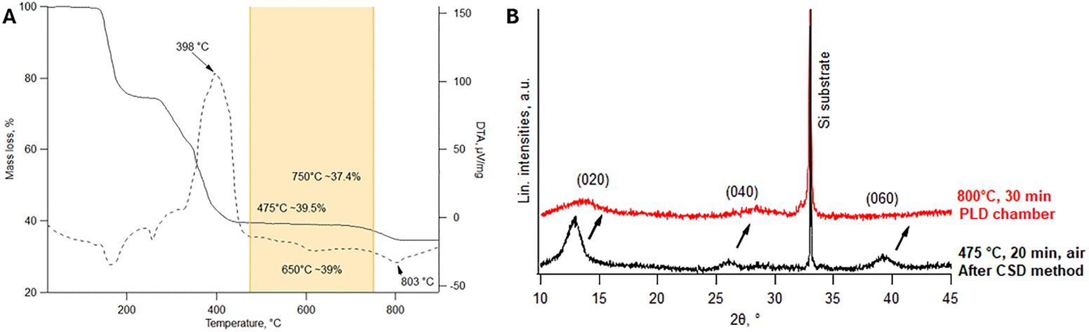 | ||
| Fig. 1 (A) TGA-DTA record of the La2O2CO3 solution with a heating ramp of 10 °C min−1 under an air atmosphere. (B) Laboratory (Cu Kα wavelength) XRD patterns of La2O2CO3-templated Si substrate before (black) and after (red) heating up in the PLD chamber. | ||
To determine the appropriate deposition and growth window for the SrTiO3 thin film, the substrate temperature during PLD deposition was set to 300 °C to form an amorphous film on the La2O2CO3-templated Si(001) substrate, using an SrTiO3 target as described in the Experimental section. The amorphous thin films were deposited at the lowest chamber pressure of around 2.1 × 10⁻⁵ mbar for 5 min and subsequently naturally cooled to room temperature under the same pressure before being removed from the PLD chamber. The SrTiO3 film is amorphous after the deposition, as no peaks of STO are observed on the ex situ XRD patterns (Fig. 2A, red line). The crystallization step is necessary to induce the formation of a crystalline SrTiO3 film. Real-time evolution of the crystallization step from the amorphous phase into polycrystalline SrTiO3 films is observed by in situ XRD (Fig. 2B) scans. At 300 °C, the films are completely amorphous with no identifiable crystalline phases. When heated to 430 °C, several diffraction peaks of the SrTiO3 cubic phase begin to appear – 2θ = 22.783° (001), 32.424° (110), 39.985° (111), and 46.485° (002). These observations indicate that polycrystalline SrTiO3 thin films start to grow from approximately 430 °C under an ambient atmosphere. Further heating to the desired temperature and under a controlled atmosphere will result in a more crystalline SrTiO3 film with a preferential orientation.
 | ||
| Fig. 2 (A) Ex situ XRD laboratory XRD patterns (Cu Kα wavelength) of the SrTiO3 thin film before (red) and after (black) heating experiments. (B) In situ XRD scan of the SrTiO3 film, measured from room temperature to 750 °C. The color scale depicts the intensity of the signal in counts. | ||
Since the SrTiO3 deposition window should lie between 475 °C and 750 °C, due to the thermal stability of the La2O2CO3 film within this temperature range, we have selected two deposition temperatures of 650 °C and 750 °C. The SrTiO3 film was deposited using either a one-step method (deposition at the target temperature for 10 min at a specific O2 pressure of 0.13 mbar) or a two-step method (initial deposition at 300 °C for 1 min at the lowest pressure of 2.1 × 10⁻⁵ mbar, followed by a second deposition at the target temperature for 10 min at a specific O2 pressure of 0.13 mbar). The XRD patterns in Fig. 3A show that the SrTiO3 film deposited via the two-step method did not crystallize or exhibited poor crystallinity, along with cracks in the film as observed in the planar-view SEM image (Fig. 3C). These cracks indicate that the initial 20 nm thick SrTiO3 film resulted in high internal stress during crystallization due to volumetric shrinkage and lattice mismatch with the substrate. Reducing the thickness of the amorphous layer could eliminate this crack formation and should be further investigated in a follow-up study. In contrast, the one-step method resulted in good crystallinity, confirmed by diffraction peaks corresponding to (001), (110), and (200) peaks of SrTiO3, and a crack-free surface as observed in the planar-view SEM image (Fig. 3B). This indicates that the SrTiO3 film starts to grow along two orientations simultaneously. At 650 °C, the (110) orientation dominates during deposition, as (110)-oriented grains tend to nucleate first due to an unavoidable mismatch (See Fig. 3A, inset). However, this preferential orientation can be suppressed by increasing the substrate temperature to 750 °C. This behavior is attributed to differences in diffusion energy and the relaxation of internal residual strain along different orientations. A higher substrate temperature promotes the diffusion and relaxation of residual strain within (200)-oriented SrTiO3 grains, thereby gradually reducing the preferential growth of (110)-oriented grains.25 However, when the SrTiO3 film is deposited directly on the Si substrate without the La2O2CO3 film, (110)-oriented grains are formed, as shown in Fig. 3A (control experiment), due to the larger lattice mismatch and interfacial reactions between the SrTiO3 film and the Si substrate. Therefore, the La2O2CO3 film serves as an effective buffer and seed layer, promoting the desired orientation and preventing detrimental interfacial reactions.
 | ||
| Fig. 3 Laboratory (Cu Kα wavelength) XRD scans of the SrTiO3 films grown on a La2O2CO3-templated Si(100) substrate, deposited at (A) the substrate temperatures of 650 °C and 750 °C via the one- or two-step methods. Inset: XRD patterns of the (110) peak are shifted to lower 2θ positions for better visualisation of the differences between the intensities. Planar-view SEM images of the SrTiO3 film deposited via (B) one-step and (C) two-step methods. (D) XRD scans of the SrTiO3 films deposited via a one-step method at 750 °C at different oxygen pressures. | ||
As oxygen pressure plays a crucial role in SrTiO3 film growth, the films in this study exhibited a bluish color after PLD deposition, which is typically associated with oxygen-deficient SrTiO3.26 Such oxygen-deficient films are expected to form under low oxygen pressure conditions, as this is generally unavoidable.27 Therefore, different oxygen pressures (1.3, 0.13, and 2.1 × 10⁻⁵ mbar) were introduced to investigate the relative fraction of (110)-oriented grains compared to the (001)-oriented grains. Preferential orientation was evaluated based on the intensities of the (001), (110), (111), and (002) peaks from the XRD patterns (Fig. 3D) using texture coefficients TC (hkl), as defined by the Harris formula.28 The TC(hkl) values of the films grown under 0.13 mbar and 2.1 × 10⁻⁵ mbar oxygen pressure exceeded 1 for the (001) and (002) planes, indicating preferential growth along the (001) direction. In contrast, at a higher oxygen pressure of 1.3 mbar, only TC(110) was greater than 1, suggesting that higher oxygen pressure promotes growth along the (110) orientation. These results highlight the strong influence of oxygen pressure on the preferential orientation of SrTiO3 films during deposition. This effect is further supported by the Lotgering factor (LF), which quantifies the degree of preferred orientation in polycrystalline materials, with higher values indicating stronger texture.29 SrTiO3 film deposited at an oxygen pressure of 0.13 mbar exhibited an LF of 74.96%, indicating a good texture but not complete alignment along the desired orientation. In contrast, deposition under high vacuum conditions (2.1 × 10⁻⁵ mbar) resulted in an even stronger texture, with an LF of 81.22%. This difference in texture can also be explained by the influence of oxygen pressure on the ablated species during PLD, as collisions between the ablated species and oxygen molecules slow down the plume expansion. In high vacuum conditions (2.1 × 10⁻⁵ mbar), the plume expands freely, resulting in higher kinetic energy whereas higher oxygen pressure (1.3 mbar) leads to lower kinetic energy and less crystalline films.30
The θ–2θ XRD scans reveal that the SrTiO3 film exhibits a preferential out-of-plane orientation along (h00) planes. Conversely, synchrotron GIWAXS measurements, performed at shallow incident angles, probe planes that are in the Bragg condition at off-normal orientations. As a result, the 2D GIWAXS patterns for the SrTiO3 film are shown in Fig. 4A after remapping of the GIWAXS pattern (missing wedge now shown for clarity). Diffraction spots appear at specific χ angles (with 0° as the normal surface direction, i.e. out-of-plane and 90° the in-plane direction) for the different planes, proving the preferential orientation of the system. Moreover, the absence of vertical streaks from 0° to 90° confirms that the SrTiO3 film does not contain a significant fraction of randomly oriented grains. To assess the in-plane orientation, a pole figure was recorded for the (110) reflection of the SrTiO3 film at 2θ = 32.44° [Cu Kα wavelength] (Fig. 4B). The presence of a broad and arc-like intensity distribution (partial ring) at χ = 45° suggests a degree of alignment. Although this non-uniform ring might initially suggest that there are some preferred in-plane orientations, these features indicate multiple preferential orientations rather than a continuous fibre texture. This suggests that the SrTiO3 film shows some degree of ordering, which differs from the expected fibre texture of the La2O2CO3 template film. In conclusion, these observations collectively confirm a preferential out-of-plane orientation along the (00l) planes with some preferential in-plane orientation.
 | ||
| Fig. 4 SrTiO3 film deposited at 750 °C: (A) the 2D GIWAXS data and (B) the pole figure measurement of the SrTiO3 (110) plane measured with a laboratory Cu Kα source. The color scale depicts the intensity of the signal in counts per second. | ||
The structural quality of the SrTiO3 film and its interface with La2O2CO3-templated Si substrate were examined by high-resolution transmission electron microscopy (HRTEM), as shown in Fig. 5A. The cross-sectional HRTEM images reveal the crystalline SrTiO3 film grown on La2O2CO3-templated Si substrate. The presence of large interference patterns in the HRTEM image (Fig. 5B) corresponds to Moiré fringes.31 The TEM image at high magnification shows a preferential out-of-plane orientation of the SrTiO3 film, which is further confirmed by fast Fourier transform (FFT) analysis (not shown). The variation in the chemical composition across the SrTiO3 film was examined using EDX mapping in STEM mode with a high-angle annular dark-field detector. The EDX elemental maps and line profile (Fig. 5C and D) revealed a homogeneous distribution of Sr K and Ti K elements throughout the film, indicating a uniform elemental composition across the SrTiO3 film. No interfacial reaction was observed, indicating that the La2O2CO3 film is also preserved as a barrier layer to prevent the out diffusion of silicon atoms from the substrate to the SrTiO3 film at high temperature. This observation also confirms that the La2O2CO3 film does not decompose under the high kinetic energy of the ablated species during PLD.32 The SrTiO3 film thickness is approximately 42 nm after 2 minutes of PLD deposition, corresponding to a growth rate of 0.35 nm per second or 0.035 nm per pulse. Given the SrTiO3 lattice parameter of 0.3905 nm, this results in an average growth rate of 0.896 monolayer per second.
 | ||
| Fig. 5 (A) Cross-sectional HRTEM image, showing the interface between the SrTiO3 film, La2O2CO3 template layer, and the Si substrate. (B) Close-up of the SrTiO3 film. (C) EDX elemental maps and (D) the cross-sectional cumulated and normalized EDX line profile of the entire stacked layers. | ||
To demonstrate that the SrTiO3 film can serve as a texture template or transfer layer for growing a functional perovskite film, a solution-derived BaTiO3 film was deposited via the chemical solution deposition (CSD) method following the procedure in ref. 33. This resulted in a crystalline BaTiO3 film with preferential (001) orientation, as shown in the XRD patterns (Fig. 6), confirming the effectiveness of the PLD-grown SrTiO3 film as a template. However, for further implementation in targeted applications where orientation control and crystalline quality are crucial, these templates and functional films should be further investigated in follow-up studies. Such studies should include time-resolved data during the PLD deposition to monitor SrTiO3 film growth via in situ reflection high-energy electron diffraction (RHEED) and explore various PLD parameters.30,34 This combination of solution-based deposition with PLD can reduce fabrication costs and enhance high-throughput processing efficiency compared to vacuum-based techniques such as MBE. This highlights its suitability for large-area and wafer-scale fabrication and scalable integration on Si-based platforms.
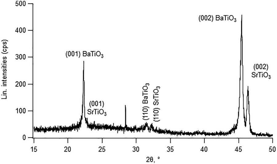 | ||
| Fig. 6 XRD patterns of the solution-derived BaTiO3 film deposited on a PLD-grown SrTiO3 film on the La2O2CO3-coated Si substrate. | ||
In summary, this work demonstrates that the La2O2CO3 film can serve as both a seed and barrier layer, providing an effective template for the integration of high-quality and textured SrTiO3 thin films on silicon substrates. Analysis of the growth windows of both materials is essential before PLD, as the stability of the solution-derived buffer layer plays a critical role. Careful control of PLD parameters, especially substrate temperature and oxygen pressure, is required to achieve preferential but not exclusive (001) out-of-plane orientation of crystalline SrTiO3 thin films. One-step PLD at 750 °C under low oxygen or vacuum pressure produced crack-free films with excellent crystallinity and uniform composition, confirmed via XRD and TEM. This confirms the potential of La2O2CO3-assisted growth strategies for integrating functional perovskite oxide films on silicon-based platforms.
Conflicts of interest
There are no conflicts to declare.Data availability
The data underlying this study is available in Zenodo at https://doi.org/10.5281/zenodo.12759437, and can be accessed freely.Acknowledgements
H. R. acknowledges support and funding as a postdoctoral fellow for fundamental research from the Research Foundation-Flanders (FWO) under grant number 1273621N. GIWAXS patterns were measured at the ALBA synchrotron facility with the collaboration of the ALBA staff.References
- E. Mikheev, B. D. Hoskins, D. B. Strukov and S. Stemmer, Resistive switching and its suppression in Pt/Nb: SrTiO3 junctions, Nat. Commun., 2014, 5, 3990, DOI:10.1038/ncomms4990.
- K. S. Randhawa, Advanced ceramics in energy storage applications: Batteries to hydrogen energy, J. Energy Storage, 2024, 98, 113122, DOI:10.1016/j.est.2024.113122.
- A. Ulrich, K. Brahim, A. Boelen, M. Debaets, A. Khalil, C. Sun, Y. Huang, S. S. Saseendran, M. Baryshnikova, P. Favia, T. Nuytten, S. Sergeant, K. Van Gasse, B. Kuyken, K. De Greve, C. Merckling and C. Haffner, Engineering high Pockels coefficients in thin-film strontium titanate for cryogenic quantum electro-optic applications, Science, 2025, 390(6771), 390–393, DOI:10.1126/science.adx3741.
- J. Haeni, P. Irvin, W. Chang, R. Uecker, P. Reiche, Y. Li, S. Choudhury, W. Tian, M. Hawley and B. Craigo, Room-temperature ferroelectricity in strained SrTiO3, Nature, 2004, 430, 758–761, DOI:10.1038/nature02773.
- S. Zhang, J. Deliyore-Ramírez, S. Deng, B. Nair, D. Pesquera, Q. Jing, M. E. Vickers, S. Crossley, M. Ghidini and G. G. Guzmán-Verri, et al., Highly reversible extrinsic electrocaloric effects over a wide temperature range in epitaxially strained SrTiO3 films, Nat. Mater., 2024, 23, 639–647, DOI:10.1038/s41563-024-01831-1.
- G. Niu, S. Yin, G. Saint-Girons, B. Gautier, P. Lecoeur, V. Pillard, G. Hollinger and B. Vilquin, Epitaxy of BaTiO3 thin film on Si (001) using a SrTiO3 buffer layer for non-volatile memory application, Microelectron. Eng., 2011, 88, 1232–1235, DOI:10.1016/j.mee.2011.03.028.
- Z. Wang, H. P. Nair, G. C. Correa, J. Jeong, K. Lee, E. S. Kim, C. S. Lee, H. J. Lim, D. A. Muller and D. G. Schlom, Epitaxial integration and properties of SrRuO3 on silicon, APL Mater., 2018, 6, 086101, DOI:10.1063/1.5041940.
- O. Nakagawara, M. Kobayashi, Y. Yoshino, Y. Katayama, H. Tabata and T. Kawai, Effects of buffer layers in epitaxial growth of SrTiO3 thin film on Si (100), J. Appl. Phys., 1995, 78, 7226–7230, DOI:10.1063/1.360433.
- M. Spreitzer, D. Klement, T. Parkelj Potočnik, U. Trstenjak, Z. Jovanović, M. D. Nguyen, H. Yuan, J. E. ten Elshof, E. Houwman and G. Koster, et al., Epitaxial ferroelectric oxides on silicon with perspectives for future device applications, APL Mater., 2021, 9, 040701, DOI:10.1063/5.0039161.
- G. Delhaye, C. Merckling, M. El-Kazzi, G. Saint-Girons, M. Gendry, Y. Robach, G. Hollinger, L. Largeau and G. Patriarche, Structural properties of epitaxial SrTiO3 thin films grown by molecular beam epitaxy on Si (001), J. Appl. Phys., 2006, 100, 124109, DOI:10.1063/1.2407273.
- M. Spreitzer, R. Egoavil, J. Verbeeck, D. H. Blank and G. Rijnders, Pulsed laser deposition of SrTiO3 on a H-terminated Si substrate, J. Mater. Chem. C, 2013, 1, 5216–5222, 10.1039/C3TC30913D.
- V. Vaithyanathan, J. Lettieri, W. Tian, A. Sharan, A. Vasudevarao, Y. Li, A. Kochhar, H. Ma, J. Levy and P. Zschack, c-axis oriented epitaxial BaTiO3 films on (001) Si, J. Appl. Phys., 2006, 100, 024108, DOI:10.1063/1.2203208.
- L. Goncharova, D. Starodub, E. Garfunkel, T. Gustafsson, V. Vaithyanathan, J. Lettieri and D. Schlom, Interface structure and thermal stability of epitaxial SrTiO3 thin films on Si (001, J. Appl. Phys., 2006, 100, 014912, DOI:10.1063/1.2206710.
- Z. Wang, B. Goodge, D. Baek, M. Zachman, X. Huang, X. Bai, C. Brooks, H. Paik, A. Mei and J. Brock, Epitaxial SrTiO3 film on silicon with narrow rocking curve despite huge defect density, Phys. Rev. Mater., 2019, 3, 073403, DOI:10.1103/PhysRevMaterials.3.073403.
- P. Dinari, C. Chandra, J. Suwardy, S. Mustofa and Y. Darma, SrTiO3 Thin Films Deposition Using Pulsed Laser Deposition Technique, Adv. Mater. Res., 2013, 789, 72–75, DOI:10.4028/www.scientific.net/AMR.789.72.
- M. D. Nguyen, H. Yuan, E. P. Houwman, M. Dekkers, G. Koster, J. E. Ten Elshof and G. Rijnders, Highly oriented growth of piezoelectric thin films on silicon using two-dimensional nanosheets as growth template layer, ACS Appl. Mater. Interfaces, 2016, 8, 31120–31127, DOI:10.1021/acsami.6b09470.
- M. Nijland, S. Thomas, M. A. Smithers, N. Banerjee, D. H. Blank, G. Rijnders, J. Xia, G. Koster and J. E. ten Elshof, Epitaxy on demand, Adv. Funct. Mater., 2015, 25, 5140–5148, DOI:10.1002/adfm.201501483.
- D. H. Blank, M. Dekkers and G. Rijnders, Pulsed laser deposition in Twente: from research tool towards industrial deposition, J. Phys. D: Appl. Phys., 2013, 47, 034006, DOI:10.1088/0022-3727/47/3/034006.
- E. Picavet, H. Rijckaert, E. Solano, O. Bikondoa, E. G. Fernandez, P. Paturi, L. Van Bossele, H. Vrielinck, J. Beeckman and K. De Buysser, The self out-of-plane oriented La2O2CO3 film: an integration tool for fiber textured ferroelectric thin films, J. Mater. Chem. C, 2023, 11, 7705–7713, 10.1039/D3TC01046E.
- J. George, P. Smet, J. Botterman, V. Bliznuk, W. Woestenborghs, D. Van Thourhout, K. Neyts and J. Beeckman, Lanthanide-assisted Deposition of Strongly Electro-optic PZT Thin Films on Silicon: Toward Integrated Active Nanophotonic Devices, ACS Appl. Mater. Interfaces, 2015, 7, 13350–13359, DOI:10.1021/acsami.5b01781.
- H. Rijckaert, Preparation of the S/TEM Lamella of Commercial REBa2Cu3O7−x Coated Conductors by FIB, IEEE Trans. Appl. Supercond., 2024, 34(7) DOI:10.1109/TASC.2024.3438690.
- H. Guerreiro, P. Melnikov, I. Arkhangelsky, L. de Oliveira, G. Wandekoken and V. do Nascimento, Thermal decomposition of lanthanum nitrate hexahydrate La(NO3)3·6H2O, Int. J. Dev. Res., 2021, 11, 43318–43321, DOI:10.37118/ijdr.20799.01.2021.
- C. Yang, H. Fan, Y. Xi, S. Qiu and Y. Fu, Anomalous phase formation during annealing of La2O3 thin films deposited by ion beam assisted electron beam evaporation, Thin Solid Films, 2009, 517, 1677–1680, DOI:10.1016/j.tsf.2008.09.069.
- A. Yadav, A. Lokhande, R. Pujari, J. Kim and C. Lokhande, The synthesis of multifunctional porous honey comb-like La2O3 thin film for supercapacitor and gas sensor applications, J. Colloid Interface Sci., 2016, 484, 51–59, DOI:10.1016/j.jcis.2016.08.056.
- J. Ye, S. Mou, R. Zhu, L. Liu and Y. Li, Orientation competition growth and mechanism of SrTiO3 film on CeO2 layer, Vacuum, 2021, 194, 110626, DOI:10.1016/j.vacuum.2021.110626.
- C. W. Schneider, M. Döbeli, C. Richter and T. Lippert, Oxygen diffusion in oxide thin films grown on SrTiO3, Phys. Rev. Mater., 2019, 3, 123401, DOI:10.1103/PhysRevMaterials.3.123401.
- H. N. Lee, S. S. Ambrose Seo, W. S. Choi and C. M. Rouleau, Growth control of oxygen stoichiometry in homoepitaxial SrTiO3 films by pulsed laser epitaxy in high vacuum, Sci. Rep., 2016, 6, 19941, DOI:10.1038/srep19941.
- M. Bannur, K. Maddani, S. Mathad and P. Patil, Structural and Optical Properties of (110) Plane Textured SnO2:Zn Thin Films, Int. J. Self-Propag. High-Temp. Synth., 2019, 28, 34–38, DOI:10.3103/S1061386219010035.
- J. L. Jones, E. B. Slamovich and K. J. Bowman, Critical evaluation of the Lotgering degree of orientation texture indicator, J. Mater. Res., 2004, 19, 3414–3422, DOI:10.1557/JMR.2004.0440.
- N. A. Shepelin, Z. P. Tehrani, N. Ohannessian, C. W. Schneider, D. Pergolesi and T. Lippert, A practical guide to pulsed laser deposition, Chem. Soc. Rev., 2023, 52, 2294–2321, 10.1039/D2CS00938B.
- X. Ke, M. Zhang, K. Zhao and D. Su, Moiré fringe method via scanning transmission electron microscopy, Small Methods, 2022, 6, 2101040, DOI:10.1002/smtd.202101040.
- M. J. Aziz, Film growth mechanisms in pulsed laser deposition, Appl. Phys. A: Mater. Sci. Process., 2008, 93, 579–587, DOI:10.1007/s00339-008-4696-7.
- E. Picavet, E. Lievens, K. De Geest, H. Rijckaert, E. G. Fernandez, O. Bikondoa, E. Solano, P. Paturi, N. Singh and T. Pannier, Integration Of Solution-Processed BaTiO3 Thin Films with High Pockels Coefficient on Photonic Platforms, Adv. Funct. Mater., 2024, 34, 2470214, DOI:10.1002/adfm.202403024.
- M. M. Aye, E. Rivasto, M. Z. Khan, H. Rijckaert, E. Salojärvi, C. Haalisto, E. Mäkilä, H. Palonen, H. Huhtinen and I. Van Driessche, Control of the nanosized defect network in superconducting thin films by target grain size, Sci. Rep., 2021, 11, 6010, DOI:10.1038/s41598-021-85304-4.
Footnotes |
| † These authors contributed equally to this work. |
| ‡ Present address: Institute of Condensed Matter Chemistry and Technologies for Energy, National Research Council of Italy (ICMATE-CNR), Via Gaetano Previati 1/E, 23900 Lecco, Italy. |
| This journal is © The Royal Society of Chemistry 2026 |