
 Open Access Article
 This Open Access Article is licensed under a Creative Commons Attribution-Non Commercial 3.0 Unported Licence
Bypassing sulfides: comparing the morphology and performance of solution processed Cu(In,Ga)Se2 films prepared via two selenide molecular precursor routes
Robert
Spilker
 a,
Daniel C.
Hayes
a,
Shubhanshu
Agarwal
a,
Kim
Kisslinger
b and
Rakesh
Agrawal
*a
a,
Daniel C.
Hayes
a,
Shubhanshu
Agarwal
a,
Kim
Kisslinger
b and
Rakesh
Agrawal
*a
aDavidson School of Chemical Engineering, Purdue University, West Lafayette, IN 47907, USA. E-mail: agrawalr@purdue.edu
bCenter for Functional Nanomaterials, Brookhaven National Laboratory, Upton, NY 11973, USA
First published on 24th November 2025
Abstract
Solution-processing of thin-film photovoltaics offers an alternative to vacuum-deposition based approaches. The amine–thiol reactive solvent system has become a focal point for the solution-processing of chalcogenide species, owing to the convenience of precursor preparation and comparatively high performance of prepared devices. Selenide species prepared via the amine–thiol route typically progress through a sulfide intermediate phase, and as such are commonly afflicted with sulfur and carbon impurities along- side the presence of a carbonaceous fine-grained layer. Here, two routes of preparing films directly to a selenide phase are examined; first by the co-dissolution of selenium in an amine–thiol solution and second via the novel use of reactive alkylammonium polyselenides. Lamella are cut from these selenide precursor films and final devices, and STEM-EDX and TEM are used to characterize film morphology and secondary phases. A champion device efficiency of 11.2% is reported for the novel polyselenide route, and clear paths of improvement are identified.
Introduction
Among solution-processed thin-film photovoltaic fabrication routes, hydrazine-based solvation stands at the forefront in terms of final device performance, absorber layer morphology, and impurity content.1 However, its use is limited due to its toxicity and portent for violent reaction. Organic solvent systems dial back the toxicity and reactivity, while generally avoiding the detrimental oxide formation that is a pitfall of the most benign routes.2,3 The amine–thiol solvent system, often labeled an alkahest for its versatility, has been extensively studied and used to produce devices reaching 16.48% conversion efficiency.4–9 This is a record among solution-processed non-hydrazine routes, yet solution processing as whole still lags behind the record setting 23.64% device recently reported via vacuum-based deposition.10 However, the reaction mechanism on which this system is based produces metal-thiolate precursors carrying alkyl groups (M–S–R), which are difficult to remove during film processing.11,12 These persistent anionic functional groups contribute sulfur and carbon impurities that the notorious fine-grained-layer is typically ascribed to. Co-dissolution of selenium has been shown to reduce or eliminate the fine-grained-layer by displacing the metal–sulfur bonds during film coating and annealing.13 Even so, thiolates are still carried through to the coated film, resulting in trace sulfur and carbon that can affect post selenization morphology and final device performance.For sulfide precursor films produced from metal-thiolate precursors, Cu(In,Ga)Se2 grain coarsening is typically nucleated at either film interface before spreading through the rest of the film.13 As this coarsened front proceeds across the depth of the film, residual carbon and other impurities are rejected from the crystal lattice, accumulating and causing the formation of the fine-grained layer.13–15 This fine-grained layer, which is nigh ubiquitous among amine–thiol processing routes, is believed to contribute to higher carrier recombination and lower performance in CIGSSe thin-film photovoltaic devices.16,17 The fine-grained layer also limits the growth of large grains, leading to a smaller average grain size and more instances of grain boundaries which are reported to act as charge transport barriers and recombination centers.18,19 An ideal absorber layer morphology would see densely packed grains that are fully coarsened from the top to bottom interfaces with a smooth top interface for the deposition of subsequent layers.
In addition to metals and metal-chalcogenides, the amine–thiol reactive solvent system is capable of dissolving elemental chalcogenides, sulfur, selenium, and tellurium. Recent investigation into these reactions revealed the formation of several polychalcogenides where the exact composition depended on both the type of amine used and the thiol to selenium ratio.20 Notably, when selenium is dissolved in a monoamine–monothiol solution, it forms a sulfur- and carbon-free polyselenide anion complexed with an alkylammonium cation. When precipitated and redissolved in select solvents, this alkylammonium polyselenide (AAPSe) is capable of facilitating reactive dissolutions of late transition metals and metal chalcogenides, having been used to prepare a CuInSe2 film and device with no sulfide intermediates, boasting an improved performance over selenide precursor films prepared by selenium co-dissolution.21,22 In this work, Cu(In,Ga)Se2 nanocrystalline films were coated directly from inks via two distinct molecular precursor routes – using amine–thiol based precursors with co-dissolved selenium and using precursor inks derived from alkylammonium polyselenides. The composition, morphology, and optoelectronic performance of films and devices prepared by these two distinct routes are then compared.
Experimental
Materials
Copper(I) selenide (Cu2Se; 99.95%), selenium powder (100 mesh, 99.99%), toluene (anhydrous, 99.8%), butylamine (BA; 99.5%), hexylamine (HA; 99%), ethylenediamine (EN; ≥99.5%), 1,2-ethanedithiol (EDT; ≥ 98%), N,N-dimethyl-formamide (DMF; 99.8%), thiourea (>99%), and gallium(III) acetylacetonate (Ga-acac; 99.99%) were purchased from Sigma-Aldrich. Indium powder (99.999%) was purchased from Strem Chemicals. Gallium pellets (99.99999%) were purchased from Alfa Aesar. 1-Ethanethiol (ET; >99%), indium(III) selenide (In2Se3; 99.99%), cadmium sulfate hydrate (CdSO4; 99.996%), and ammonium hydroxide solution in water (NH4OH; 28–30%) were purchased from Fisher Scientific. Molybdenum(IV) oxide pieces (MoO3; 99.95%), nickel pellets (99.995%), and aluminum pellets (99.999%) were purchased from Kurt J. Lesker. Sodium flouride (NaF; 99.9%) was purchased from Stanford Advanced Materials. All materials were used as received. All materials, with the exception of thiourea, cadmium sulfate, ammonium hydroxide, and the nickel and aluminum pellets, were stored in a glovebox under inert atmosphere.Butylammonium polyseleinde preparation and isolation
Butylammonium polyselenides were prepared following a modified procedure from our previous work.9,21 Selenium powder was dissolved at 4 M concentration in butylamine (BA) and ethanethiol (ET) at a BA![[thin space (1/6-em)]](https://www.rsc.org/images/entities/char_2009.gif) :ET volume ratio of 3:1, forming a dark red-to-black solution. The polyselenide was isolated via solvent-antisolvent addition and centrifugation. In a 25 mL polytetrafluoroethylene (PTFE) centrifuge tube, 1 mL of the Se-BA-ET solution was combined with 24 mL of toluene, rapidly forming a solid precipitate. The solution was then centrifuged at 14000 rpm for 10 minutes, resulting in a uniform black pellet and a transparent light brown supernatant. The supernatant was decanted and the pellet was redissolved in 1 mL butylamine. The selenium complex was isolated again via the same procedure and dried under a flow of an inert gas for 30 minutes. The remaining solid was redissolved in 2 mL of BA and used as a butylammonium polyselenide (BAPSe) stock solution with an approximate selenium-basis concentration of 2 M.
:ET volume ratio of 3:1, forming a dark red-to-black solution. The polyselenide was isolated via solvent-antisolvent addition and centrifugation. In a 25 mL polytetrafluoroethylene (PTFE) centrifuge tube, 1 mL of the Se-BA-ET solution was combined with 24 mL of toluene, rapidly forming a solid precipitate. The solution was then centrifuged at 14000 rpm for 10 minutes, resulting in a uniform black pellet and a transparent light brown supernatant. The supernatant was decanted and the pellet was redissolved in 1 mL butylamine. The selenium complex was isolated again via the same procedure and dried under a flow of an inert gas for 30 minutes. The remaining solid was redissolved in 2 mL of BA and used as a butylammonium polyselenide (BAPSe) stock solution with an approximate selenium-basis concentration of 2 M.
Precursor ink preparation
Copper and indium solutions were prepared using the BAPSe stock. In separate round-bottom flasks, Cu2Se and In powders were combined with the BAPSe stock at a metal:Se mol ratio of 1:6. Cu2Se was selected over Cu metal because it dissolved at a higher Cu:Se ratio. In2Se3 did not show appreciable dissolution in BAPSe. These flasks were connected to a Schlenk line with cold-water condensers and allowed to react at 65 °C for 5 days (Fig. S1). A low flow of Argon was used to maintain an inert environment. After 5 days, the flasks were removed from the Schlenk line and the copper-polyselenide (Cu-PSe) and indium-polyselenide (In-PSe) stock solutions were set aside for later use.
Gallium species did not exhibit appreciable solubility in BAPSe and had to be dissolved by a different method. In a round-bottom flask, 1,2-ethanedithiol (EDT) and ethylene diamine (EN) were combined with Ga metal and Se powder in an EDT:Ga:Se mol ratio of 4:1:2 and diluted with EN to target a Ga concentration 0.4 M. This solution was similarly connected to a Schlenk line and allowed to react at 65 °C for 5 days. The dissolved Ga and Se precursor species was isolated similarly via antisolvent precipitation. 2 mL of the Ga solution and 23 mL of toluene were added to a 25 mL centrifuge tube and vortexed, forming two liquid phases – a clear supernatant and a viscous, dark-colored phase containing the dissolved Ga and Se species. The supernatant was decanted, and 1 mL of BA was mixed with the remaining Ga and Se species. The centrifuge tube was again filled to volume with toluene and vortexed, with the Ga and Se species forming a mixed liquid–solid precipitate. This process was repeated until the Ga and Se species formed a solid pellet and the supernatant came out clear, typically requiring five washes. The pellet was then dried under an argon flow to remove any remaining solvent. The Ga and Se species (Ga + Se) was redissolved in BA or HA at a Ga concentration of 0.2 M assuming no losses.
Precursor inks were made by combining the Cu-, In-, and Ga- stock solutions to the target [Cu]/([Ga] + [In]) (CGI) and [Ga]/([Ga] + [In]) (GGI) atomic ratios. These ratios were confirmed via XRF prior to coating. The inks were then concentrated by evaporating the solvent under Ar flow and redissolving at half-volume. Hexylamine was used as the solvent for inks used for devices, and the final metals-basis concentration ([Cu] + [In] + [Ga]) was 0.5–0.6 M. These precursors are abbreviated as CI-PSe and CIG-PSe. Comparative inks were prepared by co-dissolving Cu2Se and In2Se3 in BA-EDT. In Ga-containing inks, the same Ga and Se species as described above were used. Inks were diluted by half with HA, to a final metals-basis concentration of 0.6 M. Because these precursors contain residual thiols and thiolates, they are referred to as sulfoselenides and abbreviated as CISSe and CIGSSe.
Device fabrication
Devices were fabricated following a SLG/Mo/CIGSe/CdS/ZnO/ITO/Ni/Al architecture. Molybdenum was deposited on a 1.8 mm thick soda-lime-glass (SLG) substrate via direct-current-magnetron sputtering to a thickness of 800 nm. Prior to film coating, 5nm of MoO3 was deposited at a rate of 0.03–0.05 Å s−1via thermal evaporation. A thin layer of MoO3 has been reported to restrict grain growth at the Mo-interface, producing a bilayer morphology instead of the commonly observed trilayer.13Cu(In,Ga)Se2 thin films were cast via a blade coating procedure to a thickness of 1.5–2.5 µm, requiring 16–24 total layers. After each layer, the film was annealed at 350 °C for 2 minutes. The film was placed on a thin sheet of graphite which was then transferred to the hot plate to prevent cracking from thermal shock. A bell jar system was used to remove any solvent or selenium vapor generated during annealing.
After coating but prior to selenization, 10 nm of NaF was deposited on select films at a rate of 0.5–1.0 Å s−1via thermal evaporation. Selenization was conducted in a 3-zone tubular furnace under an Ar atmosphere for 20 minutes at 510 °C. Films were placed in a porous graphite box and surrounded by ∼500 mg of crushed Se- pellets. The graphite box assembly was placed in the tube furnace outside of the heating zones and upstream of the vent. The furnace was allowed to reach its set-point, and an Ar flow of 0.05 SCFM was maintained during heat-up to prevent residual selenium in the furnace fittings from evaporating and contacting the films. Once the furnace stabilized within ±2 °C of the setpoint, the Ar flow was cut and the graphite box inserted into the center heating zone of the furnace. 20 minutes after film insertion, the furnace was opened and the films were allowed to cool naturally to 300 °C. A low Ar flow was provided to prevent a backflow of oxygen as the system cooled without displacing the selenium vapor cloud surrounding the graphite box. When the system reached 300 °C, the Ar flow was set to 1.0 SCFM and an external box fan was turned to the highest setting and directed at the furnace to speed up cooling via forced convection.
Following selenization, CdS was deposited via chemical-bath deposition. The films were suspended in a jacketed beaker maintained at 65 °C. A solution containing 150 mL of deionized water, 22 mL of a 0.015 M CdSO4 in water solution, and 28 mL of 30 wt% NH4OH were added and continuously stirred at 100 RPM. After 1 minute, 22 mL of a 0.75 M thiourea in water solution was added and the deposition continued for another 10 minutes. After deposition, films were rinsed with deionized water and dried in air at 125 °C. Next, 50 nm of ZnO and 150 nm of indium tin oxide (ITO) were deposited via radio frequency sputtering. Finally, patterned masks were used to apply 100 nm Ni/1000 nm Al grids via electron-beam vapor deposition. The final devices were mechanically scribed to divide individual cells each with an active area of ∼0.09 cm2.
Characterization
Raman spectroscopy and photoluminescence (PL) spectroscopy were performed using a Horiba/Jobin–Yvon HR800 Raman spectrometer with a 632.8 nm excitation laser wavelength. PL spectra were corrected with a transfer function to account for artifacts from raw data collection. All PL measurements were performed at the same conditions, with the acquisition time being shortened when necessary to avoid saturating the detector. All PL spectra are scaled to an acquisition time of 1 second.X-ray fluorescence (XRF) was performed with a Fisher XAN 250 instrument that utilized a voltage of 50 kV, a silicon drift detector, a primary nickel filter, and helium flowing as a purge gas.
X-ray diffraction (XRD) data were collected using a Rigaku SmartLab diffractometer with a Cu Kα (λ = 1.5406 Å) source operated at 40 kV/44 mA in parallel-beam mode.
Current–density vs. voltage (JV) measurements were done at 25 °C at standard AM1.5 conditions with an Oriel Sol3A solar simulator calibrated using an Oriel 91150 V silicon reference cell.
Lamella for transmission electron microscopy (TEM) were milled using a Ga-focused ion beam (FIB) on an FEI Helios 5 UX Dual Beam FIB-SEM and mounted on Cu or Mo FIB lift-out grids. Prior to the milling procedure, ∼50 nm of Pt metal was deposited onto the samples via sputtering. TEM, high-angle annular dark-field (HAADF), selected area electron diffraction (SAED), and energy dispersive X-ray spectroscopy (EDX) imaging were performed on an FEI Talos F200X scanning/transmission electron microscope (S/TEM).
Results and discussion
Precursor film characteristics
Films were prepared from four different ink formulations, summarized in Table 1. Films and inks derived from polyselenide precursors are abbreviated CI-PSe and CIG-PSe while films and inks derived from precursors dissolved directly in an amine thiol solution are abbreviated CISSe and CIGSSe.| Ink formulation | Abbreviation | CGI | GGI |
|---|---|---|---|
| Cu2Se and In2Se3 in HA-EDT | CISSe | 0.9 | 0 |
| Cu2Se, In2Se3 in HA-EDT and Ga + Se in HA | CIGSSe | 0.9 | 0.1 |
| Cu-PSe and In-PSe in HA | CI-PSe | 0.9 | 0 |
| Cu-PSe, In-PSe, and Ga + Se in HA | CIG-PSe | 0.9 | 0.2 |
n-Alkylammonium polyselenides (AAPSe) have been shown to be able to produce soluble polyselenides from a wide range of transition metals and metal-chalcogenides. Though derived from an amine–thiol solvent system, residual thiols and disulfide species are easily washed away, making the AAPSe's used for dissolution sulfur-free.21 The absence of residual thiolates means that polyselenides are free of the primary source of carbon impurities in typical amine–thiol inks.11 Still, alkylammonium cations must be considered as a potential carbon source. FTIR transmittance spectra show alkyl-carbon (CH) stretching from 3200–2700 cm−1 in thin films of butylammonium polyselenide (BAPSe) and copper polyselenide (CuPSe) dried at 25 °C (Fig. 1), but annealing, 100 °C for BAPSe and 200 °C for CuPSe, was sufficient to remove these species. Alkyl species were absent from an InPSe film following a 150 °C anneal, but the use of gallium acetylacetonate resulted in persistent carbonaceous residue (Fig. S2 and S3). The CuPSe film decomposed into Cu2−xSe following the 150 °C anneal, indicated by the change in the color of the film (Fig. S4). Ink concentration and coating solvent were both shown to affect carbon residue (Fig. 2), thus care had to be taken in developing a coating procedure that minimized carbon while still producing dense, thick films with minimal pinholes.
 | ||
| Fig. 1 FTIR transmission spectra of coated films of (a) BAPSe and (b) BAPSe-derived copper-polyselenide. | ||
 | ||
| Fig. 2 Raman spectra of films of CIG-PSe (a) coated using butylamine (BP: 78 °C), hexylamine (BP: 131 °C) and dimethylformamide (153 °C) and annealed at 225 °C and (b) coated using BA and HA as the solvent at 2× (0.5 M) and 4× (1.0 M) the as-prepared concentration. Films were annealed at 350 °C. | ||
Alkylammonium polyselenides easily dissolved in a wide range of polar organic solvents allowing for flexible coating conditions. Several solvents and ink concentrations were evaluated. Higher boiling point solvents were found to produce a stronger CIGS Raman peak, 172 cm−1, at lower annealing temperatures, 225 °C, possibly owing to a more persistent liquid medium (Fig. 2a). Forming the ternary or quaternary species is essential during film coating because binaries are readily soluble in AAPSe solutions unlike the ternary species, creating an obstacle in producing thick films. Even so, the higher boiling point solvents investigated all produced discontinuous, partially delaminated films. Hexylamine and butylamine were selected as the potential coating solvents, and a higher annealing temperature, 350 °C, was used to ensure CIGS formation. The surfaces of films coated using HA were visually more uniform (Fig. S5).
Polyselenide solutions in HA and BA readily wet molybdenum and glass substrates, but the wetting of the glass coating rod limited the overall film thickness. Increasing the ink concentration enabled the coating of a thicker film, but carbon content and film quality were sensitive to ink concentration and solvent choice (Fig. 2), with carbon peaks emerging in Raman for highly concentrated inks. Under SEM, films coated from HA at 2× concentration had relatively few pinholes and cracks (Fig. S6). The 4× concetrated inks also retained selenium beyond the stoichiometric composition after coating (Table S1). Because of this, the better visual uniformity of HA based inks, and the relatively lower intensity of residual carbon peaks in the Raman spectra (Fig. 2b), HA was selected for the coating solvent with inks concentrated to two times their dissolved concentration. Even at this total metals concentration of 0.5 M ([Cu] + [In] + [Ga]), 20–24 layers were required to reach a thickness of 2 µm. Dropcast samples at a CGI of 0.95 showed detectable CuSe binaries in XRD (Fig. S7), so the CGI was reduced to 0.9 for the coated films. XRD spectra of the sulfoselenide and polyselenide precursor films show that both are crystalline Cu(In,Ga)Se2, with no detectable binary chalcogenide species (Fig. 3).
 | ||
| Fig. 3 XRD of the coated films from sulfoselenide and polyselenide precursor inks. Reference spectra were generated from ICSD#169229 (CuIn0.85Ga0.15Se2). | ||
STEM-EDX analysis
For STEM and EDX analysis, lamella were FIB-milled to electron-transparency from the CIGSSe and CIG-PSe precursor films and devices. These lamellae were compared to cleaved cross sections of the final devices captured via SEM (Fig. S10), confirming that they are representative of the general device morphology. The unselenized CIGSSe (Fig. 4a) film exhibited a striated pattern throughout its depth that correspond to the coated layers of precursor ink. Each striation exhibits a grading of increasing density from the base to the top of an individual layer. Pores are visible throughout the film, with the largest forming at the interface between subsequent layers. No elemental gradation within layers is discernible by EDX mapping, and spectral line scans across a layer interface showed a uniform composition. Spectral analysis reveals a low-intensity peak corresponding to S, with [Se]/[S] ≈ 15.7. The substrate of the amine–thiol precursor film was not milled by the FIBing procedure. TEM revealed clear crystallites in the film, with visible crystalline domains on the order of 10–20 nm (Fig. 5a and b). SAED of the film showed the CIGSe (204) and (312) plane, with the (112) diffraction ring obscured by the beamstop (Fig. 5c). | ||
| Fig. 4 HAADF-STEM images and STEM-EDX elemental maps of the FIB-milled lamella cut from unselenized (a) CIGSSe and (b) CIG-PSe film. | ||
 | ||
| Fig. 5 A TEM image of the mid-region of the unselenized CIGSSe film at (a) x120K and (b) x390K magnification and (c) a selected area electron diffraction (SAED) pattern collected from the same region. Note that the (112) ring is obscured by the beamstop. | ||
The coated CIG-PSe film (Fig. 4b) is of a more uniform density with several large pores visible throughout the film. Individual layers are not distinct as in the sulfoselenide precursor film. STEM-EDX mapping (Fig. 4b) indicates a uniform distribution of elements. The apparent Ga-gradient is an artifact of the FIB-milling procedure, as Ga-ions accumulate with greater depth during lamellar thinning and polishing. A similar gradient is visible in the Mo substrate. Fig. 4b also shows the distribution of sulfur and carbon throughout the coated film. The strong sulfur signal in the molybdenum layer is due to the overlap of sulfur's K-α and molybdenum's L-α peaks. Emission spectra showed a weak carbon peak, but this could be a result of impurity introduction from sample handling. TEM of this film showed randomly oriented crystalline lattices on the order of 10–20 nm in size, with SAED revealing the CIGSe (112), (204), and (312) planes (Fig. 6). Note that the pre-sputtered Pt layer contributes an intense EDS signal, owing to it's larger nucleus, leading to the appearance of a Cu, S, Se, and other elements concentrating at the surface.
 | ||
| Fig. 6 A TEM image of the mid-region of the unselenized CIG-PSe film at (a) x120K and (b) x390K magnification and (c) a selected area electron diffraction (SAED) pattern collected from the same region. | ||
The structures of the selenized films differ greatly depending on the properties of their precursors. The CISSe film (Fig. 7 a) contains a range of grain sizes randomly positioned throughout the film, while the CIGSSe films with and without NaF (Fig. 7b and c) are comprised of a seemingly continuous large-grained upper region resting on isolated pillars of small grains. In the CIGSSe/NaF device, Fig. 8 shows that the small-grained region also contains several layered grains. SAED of this section (Fig. 8) shows partial diffraction bands confirming that these regions are made of CIGSe material that has retained the layered structure of the precursor film. Multiple grain orientations can be observed in Fig. 8c, indicating that these layers are only partially sintered. This is surprising, as Na doping is generally reported to enhance grain growth. A possible explanation is that, because the dopant is introduced at the upper surface, it is causing rapid crystallization of the upper grains. As a result, selenium diffusion into the film is inhibited, thus choking the liquid selenium supply at the back interface and limiting the sintering rate. The large void spaces in these films are likely a result of the low-density regions observed in the sulfoselenide precursor. The densification of precursor films through compression has been reported to improve morphology, with dense films leading to larger grains with fewer post-selenization voids or pinholes.23 Selenization conditions, such as temperature, vapor pressure, or condensation rate, also play a major role in the development of film morphology.24
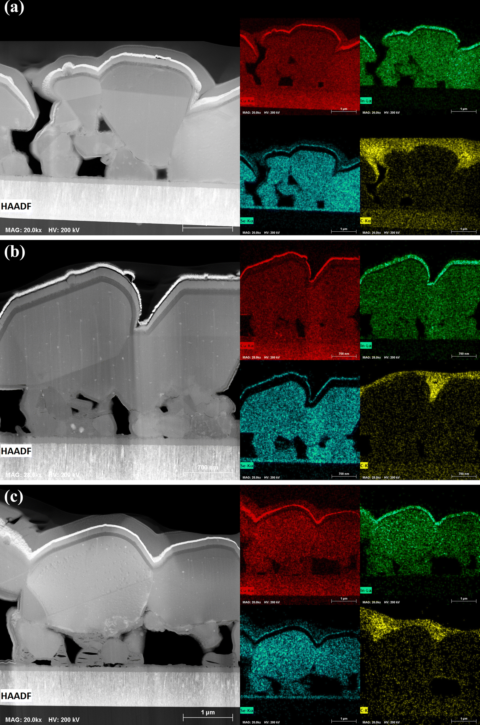 | ||
| Fig. 7 HAADF-STEM images and EDX elemental maps for Cu (red), In (green), Se (cyan), and C (yellow/orange) of FIB-milled lamella cut from the champion cells of devices made from (a) CISSe, (b) CIGSSe, and (c) CIGSSe with 10 nm NaF. | ||
 | ||
| Fig. 8 (a)–(c) TEM of the CIGSSe with NaF device capturing a partially sintered Cu(In,Ga)Se2 grain retaining its layered structure from the coating procedure and (d) SAED of the region visible in (c). | ||
A bulk growth mechanism is typically expected for selenide precursor films.13,25 Considering this, the trilayer structure of polyselenide films (Fig. 9) is an unexpected result. The sulfoselenide and polyselenide precursor films were both nanocrystalline Cu(In,Ga)Se2 with no obvious differences in crystal size or diffraction patterns (Fig. 3, 5 and 6). Bi- and trilayer structures are common in films undergoing a sulfide to selenide conversion as the newly formed selenide phase preferentially nucleates at either the back Mo interface or the front film surface. Selenide precursor films are expected to undergo a bulk growth mechanism in which nuclei formed during film coating sinter and grow.13 This is seen in the sulfoselenide precursors, and these contrasting structures hint at a difference in the precursor films leading to disparate growth mechanisms. The carbon signal observed in the fine grained layer (Fig. 9) indicates that some carbon is introduced by the precursors or the annealing procedure. It's possible that this could be eliminated by further tuning of the ink concentration or annealing conditions.
 | ||
| Fig. 9 HAADF-STEM images and EDX elemental maps for Cu (red), In (green), Se (cyan), and C (yellow/orange) of FIB-milled lamella cut from the champion cells of devices made from (a) CI-PSe, (b) CIG-PSe, and (c) CIG-PSe with 10 nm NaF. | ||
Both film types contained large voids at the rear interface. The CI- and CIG-PSe films all have large Cu2−xSe crystals that have formed in the voids along the rear interface (Fig. 10). To understand how these crystals are formed, the selenization mechanism must be discussed. Typical tube furnace selenizations can be broadly broken down into three stages: heat-up, steady-state, and cool-down. In the cooling stage of selenization, heat transfer is dominated by conduction through the substrate, leading to thermal gradients with the film surface being warmer than the surroundings, thus driving evaporation of remaining liquid selenium.26 Copper has appreciable solubility in liquid selenium, so the Cu2−xSe crystals are most likely formed from the evaporation of a Cu-enriched selenium liquid.27 This means that the polyselenide precursor films, all of which had Cu2−xSe crystals in the voids at the rear interface, likely contained some amorphous copper selenide binaries. This copper dissolution is likely linked to the tri-layer structure observed and may be encouraging interfacial nucleation.
 | ||
| Fig. 10 A (a) HAADF micrograph depicting the large Cu2−xSe crystals formed at the Mo interface from the CI-PSe device, and EDX maps for (b) Cu (red), (c) In (green), and (d) Se (cyan). | ||
Surprisingly, the thermally evaporated MoO3 layer did not inhibit the nucleation of large grained Cu(In,Ga)Se2 at the rear interface as has been seen in sulfide precursor films.13 Perhaps the MoO3 layer is selenized during coating by excess selenium or is somehow ineffective as a nucleation barrier in films already containing Cu(In,Ga)Se2 nuclei.
The fine-grained layer of the polyselenide devices are indium and gallium free, consisting primarily of a Cu2−xSe binary – identified via a fast Fourier transform (FFT) of the TEM lattices (Fig. 11) – and some trace carbon. This lamella was mounted on a molybdenum grid instead of copper so that the background emission would not interfere with measurement. Care was taken to load a TEM holder without any copper or brass components. Quantitative EDX puts the Cu:Se ratio at 3:2, and analysis of a SAED pattern from the fine-grained layer matches the spectra of Cu3Se2 (Fig. 11f). Looking to the Cu–Se binary phase diagram, Cu3Se2 is the phase expected to nucleate from liquid selenium in the range of 350–500 °C.27,28 The presence of Cu3Se2 further suggests that some copper dissolution could be occuring during the selenization of polyselenide films but not the sulfoselenide films. This is especially surprising given the Cu-poor films used in this study.
 | ||
| Fig. 11 (a) A HAADF-STEM image of the selenized CIG-PSe film's fine-grained layer and the corresponding STEM-EDX elemental maps for (b) Cu, (c) In, and (d) Se, (e) a TEM image of the boxed area in (a), and (f) an SAED image collected from the fine-grained layer. | ||
All sulfoselenide films had a CdS layer on the interior grain surfaces, as seen in Fig. 12, that is notably absent in polyselenide devices, indicating a high degree of porosity that allowed a suffusion of CdS during bath deposition. Some Cd emission is observed in the fine grain layer of the CIG-PSe films (Fig. 12e) which indicates some gaps in the upper grains allowing the chemical bath deposition (CBD) solution to reach the more porous fine-grain-layer.
 | ||
| Fig. 12 EDX maps for Cadmium of the (a) CISSe, (b) CIGSSe, and (c) CIGSSe with 10 nm NaF devices, showing Cd coating the exposed grain interiors in all sulfoselenide films. Cd EDX maps for the (d) CI-PSe, (e) CIG-PSe, and (f) CIG-PSe with 10 nm NaF devices, absent of CdS on film interiors. CdS particles are visible on the film surface in subfigures (d) and (e). Some Cd signal is observed in the fine grained layer of the CIG-PSe film. | ||
Particles of CdS were found on the surfaces of all devices and are especially prominent in Fig. 12d and e. CBD of CdS has been widely studied, and similar particles are observed in all reports using this deposition method.29–33 Hariech et al. reported that CdS CBD proceeds via simultaneous ion-by-ion and cluster-by-cluster mechanisms and that these concurrent mechanisms are favored at different temperatures.29 It's clear that there is room to optimize the CBD procedure or introduce a washing step to remove large surface particles prior to TCO deposition.
The rough surface morphology of the CI-PSe films resulted in gaps in the CdS layer that were subsequently filled by sputtered ZnO (Fig. 13). Such gaps will deteriorate the local PN-junction, and are likely sites for shunting as subsequent deposition of transparent conducting oxides (TCOs) may fill the gaps with conductive material. Thus, producing smooth films post selenization is of critical importance for future improvements to this route.
 | ||
| Fig. 13 (a) A HAADF-STEM image of a particularly rough section of the CI-PSe device's upper interface and the corresponding STEM-EDX elemental maps for (b) Cd with a discontinuity in the CdS buffer layer indicated by a red arrow and (c) Zn filling the gap left in the CdS layer. | ||
Further examination of the film interfaces were conducted using STEM-EDX and TEM imaging. Fig. 14a–c captures a continuous, ∼100 nm thick layer between the Mo substrate and CIGSe grains comprised of Mo and Se. This layer is common to all devices regardless of the precursor properties, but it is totally absent prior to selenization. TEM imaging and FFT analysis (Fig. 14d and e) showed clear lattice structures with spacings corresponding to MoSe2 and CIGSe. The formation of MoSe2 is nearly ubiquitous for Cu(In,Ga)Se2 absorbers, and is even reported to form an essential Ohmic contact at the Mo interface.34,35 The MoSe2 layers observed here are much thicker than those seen elsewhere for films selenized at similar temperatures and may be negatively impacting series resistance and device performance.36,37
 | ||
| Fig. 14 (a) A HAADF-STEM image collected at the CIGS-Mo interface from the CIG-PSe champion cell and the corresponding STEM-EDX elemental maps for (b) Mo and (c) Se, (d) a TEM image of the boxed area in (a), and (e) the FFT pattern generated from (d). | ||
Device results
The current density–voltage (JV) plots and photoluminescence (PL) spectra of the champion devices prepared from sulfoselenide films are shown in Fig. 15. The JV measurement results for all sulfoselenide devices are reported in Tables S2–S5. Gallium-free CISSe devices (Fig. 15a) exhibit more shunting behavior than their CIGSSe counterparts (Fig. 15c), including much lower reverse breakdown voltages. The CIGSSe champion device gave an active-area power conversion efficiency (PCE) of 8.6%, while the champion device with NaF is notably worse, giving a PCE of 3.6%. The CISSe device performs worse than its Ga-containing counterpart with a PCE of 5.09%, but this is the only method in which NaF improves performance, boosting the PCE to 5.94%. The starkest difference in these two devices is the effect upon JSC, with NaF improving it from 30.5 to 39.5 mA cm−2. This is an improvement over the previous report using this precursor route, although the overall shape of the JV curves are similar.13 The crossover in the JV curves of these films was not as extreme as in this prior report, with the phenomenon occurring well above the VOC. This may indicate better interfacial properties.38 The primary processing change between this and the prior report is to the selenization procedure. The selenizations share a similar time and duration, but in this case, more selenium was used and it was crushed into a powder and evenly distributed around the films instead of using pellets. The increased contact area between the crushed selenium and the graphite box would cause more vapor formation in the early stages of selenization, leading to greater selenium condensation at the film surface. More work is required to truly optimize the selenization step. | ||
| Fig. 15 (a) and (c) JV and (b) and (d) PL plots collected from the (a) and (b) CISSe champion devices and (c) and (d) CIGSSe champion devices with and without NaF, and (e) the tabulated champion device data. | ||
Under the reported processing conditions, the polyselenide devices outperform their sulfoselenide coun-terparts across the board (Fig. 15 and 16). The JV measurement results for all polyselenide devices are reported in Tables S6–S9. The CIG-PSe champion cells shows active area PCE's of 11.1% and 11.2% with NaF with a similar JSC, VOC, and FF. There is a greater difference between the CI-PSe devices, with PCE's of 7.25% without NaF and 6.17% with NaF. These devices all show reverse bias breakdown at lower breakdown voltages under illumination than in dark. The CIG-PSe device without NaF has the highest reverse bias breakdown voltage of any of the devices within this report.
 | ||
| Fig. 16 (a) and (c) JV and (b) and (d) PL plots collected from the (a) and (b) CI-PSe champion devices and (c) and (d) CIG-PSe champion devices with and without NaF, and (e) the tabulated champion device data. | ||
Sodium doping is typically associated with improved morphology and optoelectronic performance, and the addition of a thin layer of NaF improved the PL performance of all devices except for the CISSe for which it had a negligible effect. Note that some sodium may be supplied from the SLG substrate, so it cannot be claimed that any of these devices are truly sodium-free. Interestingly, the CISSe devices were also the only set of devices for which NaF addition had a net positive effect on PCE, VOC, JSC, and FF. The CISSe devices also had the greatest variability of any set of devices across all measured performance parameters (Fig. S12 and S13). NaF addition exacerbated shunting in all devices measured in this report. This effect is minor in the CIG-PSe devices with a shift in shunt resistance from 859 to 698 Ω cm2 following sodium addition. The other sets of devices experienced a greater deterioration in shunt resistance. This effect on shunting may result from sodium's morphological effect on films. Sodium is known to enhance grain growth in CIGS films, but excessive growth may lead to grain isolation and the formation of shunt pathways. As seen in Fig. 7, NaF had a significant effect on film morphology. Although exacerbated by NaF, all sulfoselenide devices showed shunting behavior under high reverse biases – similarly observed in the prior report on this precursor route.13 Optimizing the coating procedure and selenization process to produce denser, shunt free films will be critical to improving the performance of devices prepared via this precursor route.
A light-induced breakdown is observed under reverse bias in all films except for the NaF-free CIG-PSe device. NaF was shown to lower the breakdown voltage in all cases, which is consistent with the literature.39,40 A previously observed’light-shunting’ phenomenon is seen here in the NaF-doped CIGSSe champion device, however this may just be the result of a particularly intense reverse bias breakdown.13,40 The sodium-free polyselenide devices (Fig. 16a and c) exhibit a positive bias rollover and crossover phenomena just above the VOC. Crossover is also seen in all JV curves except for those of the sodium-doped CIG-PSe device, which does not exhibit either. Crossover, especially when accompanied by rollover, may be caused by minority carrier recombination at the rear interface.38 Intrinsic interfacial MoSe2, as observed in Fig. 14, is an n-type material that can create detrimental band offsets leading to poor majority carrier transport and interfacial recombination of minority carriers ultimately inhibiting device performance.41 This MoSe2 layer was observed in all devices and is a likely cause of the crossover. Several dopants, such as niobium, have been explored to change MoSe2 from n- to p-type and introduce a benevolent back-surface-field.41,42 Rollover also indicates an interfacial transport barrier.43,44 The rollover seen in the gallium-free CI-PSe device (Fig. 16a) is far less pronounced than what's observed in the sodium-free CIG-PSe device, and this phenomenon was relieved by sodium doping. The fact that the rollover was limited to polyselenide devices and is eliminated by sodium doping suggests a root cause other than the MoSe2 layer.
Conclusion
A novel chemical route based on soluble alkylammonium polyselenides is used to fabricate Cu(In,Ga)Se2 devices with minimal exposure to thiol species, thus avoiding intermediate sulfide phases. This route is compared to a previously reported method of selenide precursor preparation that produces sulfoselenide films by the addition of excess selenium to amine–thiol inks. Despite the similarities in the crystallinity and composition of the precursor films, the selenized absorber layers from these two routes had significantly different morphologies. The polyselenide films saw the reemergence of a fine grained layer composed of Cu3Se2. This, coupled with the large crystals of Cu3Se2 formed in the voids at the rear interface, points towards copper dissolution in the selenium liquid phase during selenization. This dissolution indicates an altogether different growth mechanism than the mechanism seen in their sulfoselenide counterparts. By the fabrication methods reported here, champion efficiencies of 11.2% and 8.6% were achieved for the polyselenide and sulfoselenide routes, respectively. Both selenide precursor routes were sensitive to NaF, with its addition having a detrimental effect on shunting across all films. In several cases, NaF was shown to have a deleterious effect on overall device performance despite improvements to the PL response. NaF addition had the starkest morphological effect on the sulfoselenide CIGSSe film, leading to regions of unsintered Cu(In,Ga)Se2 along the Mo interface. The rough surface morphology of some films was found to lead to discontinuities in the CdS buffer layer, and large CdS particles were found across the surface of these films. The sulfoselenide films had Cd coating their interior surfaces, indicating the formation of pores at the film surfaces connected to the subsurface voids. The addition of Ag may be explored as a means to produce denser, smoother films. All films formed a ∼100 nm thick layer of MoSe2 at the rear interface. Suppression of MoSe2 formation via the deposition of a protective layer, or doping of the rear interface to produce MoSe2 with beneficial transport properties must be investigated. Further optimization of the coating procedure to produce uniform, dense films may yield better morphologies and electronic properties. The selenization process must also be optimized in order to control the growth mechanism of these films so that a flat, continuous absorber layer can be produced.Conflicts of interest
There are no conflicts to declare.Data availability
The data supporting this article have been included as part of the supplementary information (SI). Supplementary information containing images of samples and experimental setups, XRF data tables, FTIR spectra, Raman spectra, XRD spectra, XPS spectra, SEM micrographs, and device performance data tables. See DOI: https://doi.org/10.1039/d5tc02433a.Acknowledgements
The authors acknowledge financial support from the U.S. National Science Foundation Division of Materials Research (DMR) with Grant 10001536. This research used the Electron Microscopy facilities of the Center for Functional Nanomaterials (CFN), a U.S. Department of Energy Office of Science User Facility at Brookhaven National Laboratory under Contract No. DE-SC0012704.References
- S. Suresh and A. R. Uhl, Adv. Energy Mater., 2021, 11, 2003743 CrossRef CAS.
- Y. Oh, W. Yang, J. Kim, K. Woo and J. Moon, ACS Appl. Mater. Interfaces, 2015, 7, 22570–22577 CrossRef CAS PubMed.
- J. C. W. Ho, T. Zhang, K. K. Lee, S. K. Batabyal, A. I. Y. Tok and L. H. Wong, ACS Appl. Mater. Interfaces, 2014, 6, 6638–6643 CrossRef CAS.
- J. E. Lee, K.-H. Park, J. C. Kim, T.-U. Wi, A. R. Ha, Y. B. Song, D. Y. Oh, J. Woo, S. H. Kweon, S. J. Yeom, W. Cho, K. Kim, H.-W. Lee, S. K. Kwak and Y. S. Jung, Adv. Mater., 2022, 34, 2200083 CrossRef CAS PubMed.
- K. M. Koskela, M. J. Strumolo and R. L. Brutchey, Trends Chem., 2021, 3, 1061–1073 CrossRef CAS.
- M. Xu, S. Yan, T. Liang, J. Jia, S. Yuan, D. Kou, Z. Zhou, W. Zhou, Y. Qi, Y. Meng, L. Han and S. Wu, J. Energy Chem., 2025, 100, 59–65 CrossRef CAS.
- R. Zhang, S. Cho, D. G. Lim, X. Hu, E. A. Stach, C. A. Handwerker and R. Agrawal, Chem. Commun., 2016, 52, 5007–5010 RSC.
- C. B. Walker and R. Agrawal, Chem. Commun., 2014, 50, 8331–8334 RSC.
- J. W. Turnley and R. Agrawal, Chem. Commun., 2024, 60, 5245–5269 RSC.
- J. Keller, K. Kiselman, O. Donzel-Gargand, N. M. Martin, M. Babucci, O. Lundberg, E. Wallin, L. Stolt and M. Edoff, Nat. Energy, 2024, 9, 467–478 CrossRef CAS.
- X. Zhao, S. D. Deshmukh, D. J. Rokke, G. Zhang, Z. Wu, J. T. Miller and R. Agrawal, Chem. Mater., 2019, 31, 5674–5682 CrossRef CAS.
- T. Todorov, H. W. Hillhouse, S. Aazou, Z. Sekkat, O. Vigil-Galan, S. D. Deshmukh, R. Agrawal, S. Bourdais, M. Valdes, P. Arnou, D. B. Mitzi and P. J. Dale, J. Phys.: Energy, 2020, 2, 012003 CAS.
- S. D. Deshmukh, K. G. Weideman, R. G. Ellis, K. Kisslinger and R. Agrawal, Mater. Adv., 2022, 3, 3293–3302 RSC.
- S. McLeod, E. Alruqobah and R. Agrawal, Solar Energy Mater. Solar Cells, 2019, 195, 12–23 CrossRef CAS.
- A. Javed, M. Jones, S. Campbell, S. Yerci, V. Barrioz and Y. Qu, Adv. Mater. Interfaces, 2024, 11, 2300715, DOI:10.1002/admi.202300715.
- Y. Zhao, S. Yuan, D. Kou, Z. Zhou, X. Wang, H. Xiao, Y. Deng, C. Cui, Q. Chang and S. Wu, ACS Appl. Mater. Interfaces, 2020, 12, 12717–12726 CrossRef CAS.
- J. Luo, L. Tang, S. Wang, H. Yan, W. Wang, Z. Chi, J. Gong, J. Li and X. Xiao, Chem. Eng. J., 2023, 455, 140960 CrossRef CAS.
- F. Greuter and G. Blatter, Semicond. Sci. Technol., 1990, 5, 111 CrossRef CAS.
- J. Quirk, M. Rothmann, W. Li, D. Abou-Ras and K. P. McKenna, Appl. Phys. Rev., 2024, 11, 011308 CAS.
- S. D. Deshmukh, L. F. Easterling, J. M. Manheim, N. J. LiBretto, K. G. Weideman, J. T. Miller, H. I. Kenttamaa and R. Agrawal, Inorg. Chem., 2020, 59, 8240–8250 CrossRef CAS PubMed.
- J. W. Turnley, S. D. Deshmukh, V. M. Boulos, R. Spilker, C. J. Breckner, K. Ng, J. K. Liu, J. T. Miller, H. I. Kenttämaa and R. Agrawal, Inorg. Chem. Front., 2023, 10, 6032–6044 RSC.
- S. D. Deshmukh, Unveiling the Amine–Thiol Molecular Precursor Chemistry for Fabrication of Semi-conducting Materials, PhD thesis, Purdue University Graduate School, 2021.
- G. Chen, B. Pan, L. Jin, G. Jiang, W. Liu and C. Zhu, J. Alloys Compd., 2014, 610, 20–26 CrossRef CAS.
- S. Agarwal, K. Weideman, D. Rokke, K. Catherine Vincent, D. Zemlyanov and R. Agrawal, J. Mater. Chem. C, 2024, 12, 325–336 RSC.
- D. Zhao, Q. Fan, Q. Tian, Z. Zhou, Y. Meng, D. Kou, W. Zhou and S. Wu, J. Mater. Chem. A, 2016, 4, 13476–13481 RSC.
- K. G. Weideman, Development and Characterization of Film Formation Processes Toward the Im- proved Performance of Solution-Processed Semiconducting Thin Films, PhD thesis, Purdue University Graduate School, 2022.
- K. Cohen, J. Rivet and J. Dugue, J. Alloys Compd., 1995, 224, 316–329 CrossRef CAS.
- J. Y. C. Liew, Z. A. Talib, Z. Zainal, M. A. Kamarudin, N. H. Osman and H. K. Lee, Semicond. Sci. Technol., 2019, 34, 125017 CrossRef CAS.
- S. Hariech, M. S. Aida, J. Bougdira, M. Belmahi, G. Medjahdi, D. Geneve, N. Attaf and H. Rinnert, J. Semicond., 2018, 39, 034004 CrossRef.
- M. Kim, S. Lee and S. Sohn, Thin Solid Films, 2011, 519, 1787–1793 CrossRef CAS.
- W. G. C. Kumarage, L. B. D. R. P. Wijesundara, V. A. Seneviratne, C. P. Jayalath and B. S. Dassanayake, Proc. Eng., 2016, 139, 64–68 CrossRef CAS.
- V. D. Moreno-Regino, F. M. Castaneda-de-la-Hoya, C. G. Torres-Castanedo, J. Marquez-Marın, R. Castanedo-Perez, G. Torres-Delgado and O. Zelaya-Angel, Results Phys., 2019, 13, 102238 CrossRef.
- A. S. Najm, H. S. Naeem, H. S. Majdi, S. A. Hasbullah, H. A. Hasan, K. Sopian, B. Bais, H. J. Al- Iessa, H. A. Dhahad, J. M. Ali and A. J. Sultan, Sci. Rep., 2022, 12, 15295 CrossRef CAS PubMed.
- H.-Y. Sun, P.-H. Li, Y.-M. Xue, Z.-X. Qiao and L. Sai, Optoelectron. Lett., 2019, 15, 428–434 CrossRef.
- X. Zhu, Z. Zhou, Y. Wang, L. Zhang, A. Li and F. Huang, Solar Energy Mater. Solar Cells, 2012, 101, 57–61 CrossRef CAS.
- D. Abou-Ras, G. Kostorz, D. Bremaud, M. Kalin, F. V. Kurdesau, A. N. Tiwari and M. Dobeli, Thin Solid Films, 2005, 480–481, 433–438 CrossRef CAS.
- Y.-C. Lin, Y.-T. Hsieh, C.-M. Lai and H.-R. Hsu, J. Alloys Compd., 2016, 661, 168–175 CrossRef CAS.
- R. Scheer and H.-W. Schock, Chalcogenide Photovoltaics: Physics, Technologies, and Thin Film Devices, 1st edn, Wiley, 2011 Search PubMed.
- S. Puttnins, S. Jander, A. Wehrmann, G. Benndorf, M. Stolzel, A. Muller, H. Von Wenckstern, F. Daume, A. Rahm and M. Grundmann, Solar Energy Mater. Solar Cells, 2014, 120, 506–511 CrossRef CAS.
- S. Puttnins; M. Purfurst; M. Hartung; H.-K. Lee; F. Daume; L. Hartmann; A. Rahm; A. Braun and M. Grundmann, 27th European Photovoltaic Solar Energy Conference and Exhibition; 2219-2221 2012, Artwork Size: 3 pages, 6049 kb Medium: application/pdf Publisher: WIP, 3 pages, 6049 kb.
- Y. Song, B. Yao, Y. Li, Z. Ding, H. Sun, Z. Zhang, L. Zhang and H. Zhao, ACS Appl. Mater. Interfaces, 2019, 11, 31851–31859 CrossRef CAS PubMed.
- M. S. Islam, C. Doroody, T. S. Kiong, K. S. Rahman, A. W. M. Zuhdi, B. K. Yap, M. N.-E. Alam and N. Amin, Mater. Sci. Semicond. Process, 2024, 182, 108721 CrossRef CAS.
- X. Li, K. Shen, Q. Li, Y. Deng, P. Zhu and D. Wang, Sol. Energy, 2018, 165, 27–34 CrossRef CAS.
- T. Kato; K. Kitani; K. Tai; R. Kamada; H. Hiroi and H. Sugimoto, 32nd European Photovoltaic Solar Energy Conference and Exhibition; 1085–1088, 2016, 4, 4870.
| This journal is © The Royal Society of Chemistry 2026 |