
An unbalanced load resistor for ideal logic levels and maximum gain in organic electrochemical transistor-based unipolar inverters
Marcos
Luginieski
 *ab,
Bruno Bassi Millan
Torres
a,
Bianca de Andrade
Feitosa
a,
Gerwin
Dijk
c,
Alberto
Salleo
c and
Gregório Couto
Faria
*a
*ab,
Bruno Bassi Millan
Torres
a,
Bianca de Andrade
Feitosa
a,
Gerwin
Dijk
c,
Alberto
Salleo
c and
Gregório Couto
Faria
*a
aSão Carlos Institute of Physics, University of São Paulo, PO Box 369, 13560-970, São Carlos, São Paulo, Brazil. E-mail: mluginieski@ifsc.usp.br; gcfaria@ifsc.usp.br
bInstitute for Microsensors, Actuators and Systems, University of Bremen, 28359, Bremen, Germany
cDepartment of Materials Science and Engineering, Stanford University, Stanford, CA 94305, USA
First published on 10th November 2025
Abstract
Organic electrochemical transistors (OECTs) have garnered significant attention in recent years due to their unique ion-to-electron transduction capability. These devices operate by inducing ionic swelling in the channel, leading to doping/dedoping processes that result in high current density with low operating voltages. Among numerous OECT-based applications, unipolar inverters have gained attention in the last few years due to their useful application in logic structures, mainly as building blocks in neuromorphic computing. Although OECT-based inverters have shown promising gain and voltage-transfer characteristics, guidelines for circuit designs to optimize their performance are missing. Here, we explore the influence of circuit design, operating voltages and load resistance on the output logic levels and maximum gain for two well-known organic semiconductors: PEDOT:PSS and P3HT. Our results demonstrate a non-intuitive relationship between the inverter and OECT voltages caused by the initial channel conductivity. Additionally, the influence of the load resistance on the logic levels and maximum gain is examined, revealing a trade-off between achieving ideal logic levels and maximizing gain. These findings provide an overview of critical design parameters and their impact on the inverter operation, which can guide the engineering of OECT-based complex circuits, such as artificial neurons.
1 Introduction
Since the late 2000s, organic electrochemical transistors (OECTs) have gained significant attention from a diverse scientific community due to their unique ion-to-electron transduction capability.1,2 This process relies on the organic transistor channel that is interfaced by an electrolyte. Upon application of gate voltages, the doping state of the semiconducting material is changed, yielding modulation of the channel current (see Fig. 1(a) and (b)).3,4 Such switching characteristics, coupled with advances in material engineering and an improved understanding of the physical chemistry fundamentals of the device's working mechanism, have enabled their application in a wide range of fields, such as neuromorphic computing, biosensing, and logical computing, to name a few.5–10 Among these, logical computing, for instance, involves circuits ranging from simple to complex arrangements of electrical elements, designed to perform logical operations. One of the most common applications is the amplification of microvolts electrophysiological signals with relatively simple circuits.11–14 Another common use of logical devices is in ionic sensing,15,16 in which incremental changes in ion concentration can be detected and amplified. More sophisticated arrangements of logical circuits were already reported in the technical literature, as integrated circuits17 and, more recently as artificial neuron networks.6,9 | ||
| Fig. 1 (a) OECT basic structure illustration. (b) Transfer curve of a transistor in the semi-log scale. Note that the device is turned on (high current) as VGS increases. (c) The load resistor unipolar inverter with the OECT grounded (top) and with the resistor grounded (bottom). (d) Voltage-transfer characteristics (VTCs) of the inverter. (e) The output characteristics of a transistor where the dashed line represents the inverter operation. The slope is 1/Rld. (f) The inverter gain, following a bell-shaped profile. | ||
Indeed, the fundamental building blocks for data processing and storage in modern computing electronics are inverter devices. They take advantage of the voltage-controlled switching characteristic of transistors to perform binary operations. For instance, inverters are commonly used to achieve a NOT gate that inverts a high/low input into a low/high voltage output. In such a logic gate, the input and output voltages represent logical, binary states that are represented by 0's and 1's. Beyond that, inverter circuits can also be used as voltage amplifiers due to the steep inversion of the input signal.
Two main types of inverter circuits can be distinguished: the unipolar inverter, which consists of a switching transistor and a load element (either a resistor or another transistor), and the complementary inverter, which employs two active elements of opposite polarity.18 Among these, unipolar inverters represent the simplest configuration, offering versatile design and ease of fabrication. To date, numerous p-type OECT-based unipolar inverters have been reported in the literature.17,19–23 The most traditional and straightforward design consists of a transistor connected in series with a single load resistor (see Fig. 1(c)), giving rise to the so-called load-resistor unipolar inverter, also referred to as a common-source amplifier circuit.8,19–21 More sophisticated approaches have also been demonstrated, including ladder-type unipolar inverters based on one OECT and three resistors,17,22 as well as more complex arrangements involving multiple transistors and resistors.23 These advanced circuits allow for improved control over inverter gain and transient response. Finally, unipolar inverters can also be implemented by connecting two transistors of the same polarity in series, where one transistor replaces the load resistor in a feedback-gate configuration.
In terms of performance, all these circuits share common parameters and metrics. While the main characteristics of unipolar inverters will be addressed in detail in the following section, the importance of voltage gain, logic-level stability, and power dissipation is worth highlighting. For the load-resistor unipolar inverter, all these characteristics obviously depend on the chosen load resistance (Rld). Therefore, understanding how Rld affects and tunes circuit behavior is fundamental for effective implementation and optimization. Indeed, the impact of load resistance on output logic levels has been established for a resistor-ladder circuit,23 whereas the simplest load-resistor design remains largely unexplored. Moreover, the relationship between maximum gain, load resistance, and the OECT operation regime has previously been studied only for depletion-mode transistors (initially doped) and for a limited range of Rld.19 As such, the current literature presents incomplete knowledge regarding the simplest load-resistor unipolar inverter design.
In the present study, we aim to fill this gap by exploring the relationship between inverter circuit design and OECT operation, and by demonstrating an optimized strategy to maximize gain while maintaining stable logic levels. Two different organic semiconductors with distinct initial doping levels are explored: poly(3,4-ethylenedioxythiophene)polystyrene sulfonate (PEDOT:PSS, doped) and poly(3-hexylthiophene-2,5-diyl) (P3HT, undoped). First, using OECT- and resistor-grounded circuits with PEDOT:PSS-based OECTs, we investigated the relationship between the circuit configuration and OECT voltages. Our results show that the ground reference can fundamentally change OECT operation within the circuit, potentially leading to misleading interpretations of inverter behavior. This effect is also dependent on the initial semiconductor resistivity.
Subsequently, we studied the influence of load resistance on logic levels and maximum gain for both PEDOT:PSS- and P3HT-based inverters. The results reveal the existence of an optimum load resistance where both logic levels (low and high) approach ideal values. However, this optimal resistance does not correspond to the highest achievable gain. Consequently, there exists a trade-off between selecting a load resistance that favors ideal output levels versus one that maximizes gain. This trade-off must be considered when applying unipolar inverters in high-performance computing applications.
2 Inverter operation mode and main characteristics
Before delving deeper into the gaps addressed by this work, we provide an overview of the operation of load-resistor unipolar inverters and their key characteristics. Inverters are transistor-based circuits that, as the name suggests, convert a high/low input signal into a low/high output signal. This is possible due to the capability of transistors to work as voltage-controlled switches, where the current modulation directly depends on the voltage applied at the gate electrode (VGS) (see Fig. 1(b)). As VGS varies, the device changes from its initial OFF state (low current, high channel resistance) to an ON state (high current, low channel resistance), or vice versa. Therefore, when the transistor is OFF, it works as an open switch in the circuit, not allowing current to flow from the source to the drain electrodes. Conversely, when the channel resistance is low, sufficient current flows through the transistor, which is said to be in its ON state, behaving as a closed switch. In this scenario, the voltage potential drops only across the load resistor. The circuit design of two unipolar inverters is depicted in Fig. 1(c). Note that the difference between them is only the ground reference in the circuit.The inversion characteristics of these circuits are analyzed through the voltage-transfer characteristic (VTC) curve. In this curve, the output voltage (Vout) is plotted versus the input voltage (Vin) for a given supply voltage (Vdd). As depicted in Fig. 1(d), when Vin is small (close to zero), Vout is high and remains constant, known as the high level. As the input voltage increases, the output signal starts to decrease until it reaches a new constant level at low voltages, named the low level. These two levels, referred to as logic levels or logic states, can be translated as the binary operations 1 and 0. For this reason, inverters give rise to the simplest logic gate, the NOT gate, where the input signal is always inverted from 1 to 0 or vice versa.18 The VTC curve has, then, the shape of a step function, where, effects such as power dissipation, charge trapping, and parasitic capacitances, among others, lead to a smoother inversion profile, as depicted in Fig. 1(d). This highlights the main disadvantage of unipolar inverters, as their complementary counterparts exhibit sharper inversion, which translates into better voltage amplification.
The operation of a unipolar inverter can be better understood by analyzing the output characteristics of the transistor. Considering the OECT-grounded circuit design shown in Fig. 1(c), the relationship between output and drain voltages is given by:18
| Vout = VDS = Vdd − RldIDS. | (1) |
One of the most important parameters used to characterize the operation of an inverter is the unit's gain (Gn). This parameter defines the rate variation of Vout with respect to Vin, quantifying the sharpness of the transition between the two logic states. Mathematically, Gn can be expressed as:
 | (2) |
As shown in Fig. 1(f), Gn follows a bell-shaped function, where the width and height indicate how “fast” the inversion occurs. Ideally, Gn displays a high and narrow profile, which is associated with sharp inversion and the inverter's ability to amplify the input signal.
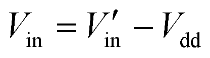
As shown in Fig. 1(b), the transistor's switching characteristics directly depend on the gate voltage, which, in turn, can be seen as a function of the input voltage for inverters. It is important to highlight that depending on the convention used, Vin does not have the same values as VGS. In the top circuit depicted in Fig. 1(c), with the OECT's source electrode connected to the ground, the input voltage is the same as the OECT's gate voltage, i.e., Vin = VGS. However, changing the ground electrode position, following the bottom circuit of Fig. 1(c), leads to a shift of the gate voltage reference, leading to VGS = Vin − Vdd. Thus, the ground position within an inverter circuit is critical for its operation. To make it clear, the next section delves into details regarding the relationship between the inverter characteristics and OECT voltages, especially for depletion-mode OECTs.
3 Results
3.1 Depletion-mode OECT-based inverters: the importance of circuit ground reference
One of the most used materials in OECT applications is the PEDOT:PSS, a p-doped organic semiconductor.1,7,24–29 As a doped material, PEDOT:PSS-based OECTs have a low initial channel resistivity (ρ0), which for the devices from the present study is roughly 10−2 Ω cm. The OECT steady-state characteristics, such as the current versus voltage curve, are shown in Fig. S1 in the SI. Unipolar inverters based on PEDOT:PSS OECTs have already been reported in the literature as voltage amplifiers and transducers.19,20 Typically, the OECT-grounded configuration is used in these works (top circuit in Fig. 1(c)). However, they have not thoroughly explored relationships between the OECT characteristics and the inverter operating voltages and output. For the OECT-grounded configuration, it is true that Vin = VGS, and when Vin ≤ 0 V the OECT acts as a closed switch, leading to Vout ≈ 0 V. As Vin increases to positive values, the channel becomes more resistive and the OECT acts as an open switch, leading to Vout = Vdd. Consequently, this circuit does not work as a true inverter for both positive and negative Vdd – once a low input signal leads to a low output level and, similarly, a high input signal leads to a high output level.To better illustrate it, Fig. 2(a) shows the VTC traces obtained for a PEDOT:PSS-based circuit with a load resistor of 100 kΩ, in the OECT-grounded configuration. Using common operational voltages for PEDOT:PSS-based OECTs, the VTC curve exhibits a similar shape to that of a step function with two distinct logic levels. However, when Vin ≈ 0, Vout remains near zero, and when Vin is high, |Vout| also increases, as expected, not representing an inverter behavior, since low input voltage also leads to a low output voltage.
 | ||
| Fig. 2 Electrical characteristics of a PEDOT:PSS-based unipolar inverter. (a) VTCs (solid lines) and gain (dashed lines) for OECT-grounded configuration. (b) The grounded resistor inverter and the respective VTCs (solid lines) and gain (dashed lines) for the resistor-grounded configuration. (c) VTCs (solid lines) and gain (dashed lines) from the two previous cases at the same reference, where the blue lines come from the OECT-grounded and the red come from the resistor-grounded configurations. For all cases, Rld = 100 kΩ. | ||
Following eqn (1), the initial low channel resistivity of the PEDOT:PSS-based OECTs (at the vicinity of Vin ≈ 0 V), results in a high drain current, making RldIDS ≈ Vdd, and thus Vout ≈ 0. As Vin increases, dedoping of the PEDOT:PSS raises the channel resistivity, reducing IDS and making the second term of eqn (1) negligible, leading to Vout ≈ Vdd. Despite its step-function-like behavior, this PEDOT:PSS-based circuit in the OECT-grounded configuration does not meet the criteria for a true inverter, although it can be employed as a voltage amplifier.19,20
It is, therefore, clear that the initial resistivity of the OECT channel is an important factor when designing and proposing inverter circuits. In fact, it is possible to obtain real inverters using PEDOT:PSS-based OECTs, by simply switching the ground electrode position, i.e., the load resistor becomes grounded, and Vdd is now applied at the OECT source electrode, being in a so-called resistor-grounded configuration.
In this case, the gate voltage can be written as
| VGS = Vin − Vdd, | (3) |
| Vout = −RldIDS. | (4) |
Comparing the inverter output of Fig. 2(a) and (b) (OECT-grounded vs. resistor-grounded), it becomes evident that curves for the OECT-grounded circuit are shifted by Vdd, and are otherwise identical to those for the resistor-grounded configuration. Using eqn (3) and noting that Vin = VGS for the OECT-grounded, one has
 | (5) |
 is the input voltage for the resistor-grounded circuit. Similarly, for the output voltage,
  . Applying this reference shift to the VTCs in Fig. 2(a) results in nearly identical VTCs and gain for both circuits, indicating that the only difference is, indeed, a voltage shift (see Fig. 2(c)). This confirms that both measurement configurations for PEDOT:PSS-based circuits lead to the expected ladder-shape function, however, only the resistor-grounded circuit exhibits the characteristics of a real inverter. Although the OECT-grounded circuit may be unsuitable for logical operations with low initial resistivity materials, it enables their operation as voltage amplifiers, having input voltages aligned with typical OECT measurement conditions.
Looking from the perspective of the initial channel resistivity (ρ0), the OECT-grounded circuit would work for OECTs with an initially dedoped channel, such as P3HT (accumulation-mode OECTs). In this case, the channel has a high initial resistance (roughly 8 MΩ for our devices, see Fig. S2 in the SI) that decreases as ions swell the semiconducting channel. In Fig. 3, the VTCs and the gain of a unipolar inverter based on a P3HT OECT with a 1 MΩ load resistance are shown. In this case, both Vin and Vdd are similar to VGS and VDS used to operate P3HT-based OECTs. Despite both PEDOT:PSS and P3HT being p-type materials, the differences in the inverter circuit design arise from the different initial doped state of these materials (depletion and accumulation mode nature), being one of the key parameters to consider when designing OECT-based inverters. Table 1 depicts a summary of the circuit design and the relationship between OECT and inverter voltages for both p-type materials.
 | ||
| Fig. 3 VTCs (solid lines) and gain (dashed lines) of a P3HT-based unipolar inverter with a Rld = 1 MΩ in the OECT-grounded configuration. | ||
| Channel | ρ 0 | Inverter circuit | Voltage relationship |
|---|---|---|---|
| Initially doped | Low | R ld grounded | V GS = Vin − Vdd |
| V DS = Vout − Vdd | |||
| Initially de-doped | High | OECT grounded | V GS = Vin |
| V DS = Vout |
3.2 Unipolar OECT-based inverters: the load resistance dependency
So far, the discussion has been focused on the circuit design for different channel materials, with no attention given to the choice of load resistance (Rld). The load resistance is an important parameter that directly impacts the inverter's logic levels, gain, and switching speed.19,22,23 From the VTCs depicted in Fig. 2(b) and 3, the logic levels deviate from ideal values. For example, in P3HT-based inverters, when Vin is approximately 0 V, the output voltage should be equal to Vdd, but the VTCs always show lower output signals. The deviation from the expected value also occurs for the low level of PEDOT:PSS-based inverters, as seen in Fig. 2(b). Here, Vout is greater than the expected zero.Therefore, to investigate the effects of the load resistance on the inverter operation and output, VTCs of PEDOT:PSS- and P3HT-based inverters were recorded for Rld ranging from 1 MΩ to 5 kΩ.
For PEDOT:PSS-based inverters, high resistances lead to high level output (Vout,H) close to the desired Vdd voltage, while the low level (Vout,L) deviates from the ideal value of 0 V (see Fig. 4(a)). Such deviation increases with the load resistance and was already previously reported for a PEDOT:PSS-based inverter with a resistor ladder.17,22,23 In contrast, however, for low Rld, Vout,H diverges from Vdd and Vout,L reaches values close to the ideal one.
 | ||
| Fig. 4 (a) VTC, (b) gain and (c) mean logic level curves for different load resistances for PEDOT:PSS-based inverters. (d) VTC, (e) gain and (f) mean logic level curves for different load resistances for P3HT-based inverters. The dashed black line on (c) and (f) indicates the ideal values, while the solid lines are the theoretical fitting. From fitting of (c) Ron = (2.4 ± 0.3) kΩ and Roff = (1.29 ± 0.04) MΩ, while for (f) Ron = (292 ± 26) Ω and Roff = (12.9 ± 0.5) MΩ. For all fittings r2 = 0.9. | ||
In P3HT inverters, the opposite effect is observed: Vout,H deviation increases with Rld, while Vout,L decreases with the load resistance, as shown in Fig. 4(d). Furthermore, the gain is also affected by Rld for both materials, as shown in Fig. 4(b) and (e), and will be addressed in the subsequent discussion.
To analyze the relationship between the logic levels and the load resistance, the mean values of Vout,H and Vout,L were plotted as a function of Rld. The Vout,H and Vout,L × Rld traces for PEDOT:PSS- and P3HT-based inverters are presented in Fig. 4(c) and (f), respectively. The right and left axes of each graph were scaled to keep both expected output values aligned (indicated by the dashed line). In both cases, an exponential-like behavior of both logic levels is observed, however, with opposite concavity. The two logic levels present regions that diverge from the expected Vout,H and Vout,L for specific load resistances. For instance, in PEDOT:PSS-based devices, Vout,H diverges for low Rld, while Vout,L diverges for high Rld. Conversely, for P3HT, the divergence of logic levels occurs opposite to that of PEDOT:PSS-based inverters. These results indicate that in real devices, it is not possible to obtain, for the same load resistance, both low and high ideal logic levels, suggesting the existence of an optimized Rld value that approximates devices to operate close to the nominal theoretical of Vout,H and Vout,L.
The determination of the output levels can be done by defining Vout,H and Vout,L in terms of the load resistances, following a similar approach from Zabihipour et al.22,23 for a resistor ladder inverter. Using eqn (1) and (4), for P3HT- and PEDOT:PSS-based inverters, respectively, and Ohm's and Kirchhoff's laws follow that
 | (6) |
 | (7) |
 | (8) |
 | (9) |
| R ch,0 | R on | R off | R ld,opt | |
|---|---|---|---|---|
| PEDOT:PSS | (1.4 ± 0.2) × 103 | 2.4 ± 0.3 | 1.29 ± 0.04 | 55.6 |
| P3HT | (7.8 ± 1.2) × 106 | 0.29 ± 0.03 | 12.9 ± 0.5 | 61.6 |
| (Ω) | (kΩ) | (MΩ) | (kΩ) |
Analysis of Fig. 4(c) and (f) reveals an intersection point, where both logic levels are simultaneously close to the desired values. This allows for the determination of an optimum load resistance (Rld,opt), where
 | (10) |
So far, the characteristics of the voltage transfer curve have been analyzed in terms of individual logic levels. A complete description of a VTC curve is not trivial, because it requires full characterization of the electric current in the circuit, which in this case can be simply described in terms of the OECT's IDS. One of the first well-established OECT models, the Bernards and Malliaras model,3 lacks explicit equations for the drain current in the saturation regime of OECTs. Since the inverter's operation involves transitions between different modes (linear to saturation), a comprehensive description of both the linear and saturation regimes of the transistor is required. Recently, a new model was proposed based on electrochemical principles to describe transistor modulation through non-ideal Nernstian reactions between ionic species and the channel material.4 Feitosa and co-authors derived the following equation for the drain current of p-type materials, which fully describes the output characteristics of OECTs:
 | (11) |
By considering eqn (11) along with eqn (1) for accumulation-mode devices and eqn (4) for depletion-mode devices, it was possible to describe all VTC and gain curves for each inverter, as depicted in Fig. 5(a) and (d) (details in Section S4 in the SI). For PEDOT:PSS-based inverters, the fitting resulted in σ0 = (0.14 ± 0.01) S cm−1, leading to Roff = 0.6 MΩ. For P3HT-based inverters, σ0 = (1.8 ± 0.2) mS cm−1, corresponding to Roff = 21.7 MΩ. These calculated resistances are in good agreement with those in Table 2.
 | ||
| Fig. 5 VTC, gain and the maximum gain curves from Fig. 4 (dots), for PEDOT:PSS (a)–(c) and for P3HT (e) and (f), respectively. The solid lines on (a) and (d) indicate the fitting. Fitting parameters are available in Table S2 in the SI. The solid lines on (b), (c), (e) and (f) are the back-calculated curves from the fitting of VTC curves. For all fittings r2 = 0.9. | ||
Moreover, from Fig. 5(c) and (f), the maximum gain for both cases follows a similar trend, despite not having the exact same values. Braendlein et al. showed that the maximum gain depends on the channel's transconductance and the load resistance.19 Additionally, it exhibits different behaviors depending on the OECT regime of operation. Zabihipour et al. also demonstrated that, for a resistor ladder-type inverter, the gain scales with the load resistance.22,23 The gain equation is defined as  and can be derived from the total differential of the drain current. The step-by-step development of the gain equation is presented in Section S5 in the SI, and is given by:19
 | (12) |
To reveal the gain behavior in relation to the inverter and the OECT characteristics, it is necessary to expand gm and gd in eqn (12) in terms of applied voltage. This requires revisiting the OECT's drain current equation, as defined in eqn (11). Given that gm and gd are defined in terms of IDS, both can be rewritten using eqn (11), as shown in eqn (S18) and (S19) in the SI. By substituting these equations into eqn (12), the inverter's gain can be written in terms of the OECT characteristics and voltages, allowing the usage of eqn (12) to reconstruct and understand the gain behavior in Fig. 5(b)–(c) and (e)–(f).
From Fig. 5(c), the maximum gain exhibits a clear parabolic dependence on the load resistance. A similar parabolic trend in the maximum gain of a PEDOT:PSS-based inverter was previously reported by Braendlein19 and attributed to the OECT operating in the linear regime. However, their study explored load resistances only up to 10 Rld/Rch,0, without observing a reduction in gain at higher load resistance values. Calculating gm and gd corresponding to the maximum gain in Fig. 5(c), using eqn (S18) and (S19), from the SI, along with the fitted parameters, obtained from Fig. 5(a) and (d), reveals that for Rld < 100 kΩ, the inverter operates near the linear regime of the OECT, with a nonzero conductance. For resistances equal to or greater than 100 kΩ, gd is negligible, indicating that the OECT is operating in the saturation regime. In this case, despite gd → 0, Gn does not increase linearly with Rld as expected from eqn (12). This deviation is due to the high residual conductivity observed in the PEDOT:PSS-based inverter, which limits the steep inversion by reducing the difference between the two logic levels.
As for the P3HT-based inverter, conversely, Fig. 5(f) shows a linear trend in the maximum gain with load resistance. Calculations reveal negligible conductance in this case, indicating operation in the transistor's saturation regime. Moreover, because of the small σ0, due to the P3HT neutral pristine state, this device exhibits a lower divergence between logic levels, which does not negatively impact the gain behavior. These results show that not only the OECT's mode of operation and the load resistance determine the inverter's gain, and must be evaluated when constructing highly efficient OECT-based inverters, but also the OFF resistance of the OECT's active layer is crucial for building inverters with high amplification capability.
The effects of the supply voltage, load resistance, and model parameters on the inverter operation are provided in Section S6 of the SI. Finally, a discussion on static power consumption as a function of load resistance, the OECT mode of operation and maximum gain is provided in Section S7 of the SI.
4 Conclusions
This study examined the fundamental aspects of unipolar inverters based on organic electrochemical transistors (OECTs). It elucidated the circuit design and the relationship between OECTs and inverter voltages concerning the initial channel resistance. For materials with high Rch,0, like P3HT, the inverter's input and output voltages directly correspond to the gate and drain voltages of the OECT. Conversely, for materials with low Rch,0, such as PEDOT:PSS, the OECT voltages are offset from the inverter ones by the inverter supply voltage. These findings lay the groundwork for the correct configuration of inverter circuits using various organic semiconductors. Additionally, we investigated the relationship between load resistance and inverter operation, demonstrating and modeling deviations from ideal output logic levels as Rld varies for both PEDOT:PSS and P3HT inverters. The greater deviation observed in PEDOT:PSS-based inverters is directly linked to the residual conductivity of the channel. An optimal load resistance was modeled based on the ON and OFF resistances of the channel. Furthermore, the results revealed a trade-off between optimum logic levels and maximum gain. In the saturation regime, the expected linear increase of gain with load resistance may be harmed due to the low difference in logic levels, a direct effect of the non-negligible residual conductivity of some devices. Conversely, devices with low σ0 values result in an enhanced maximum gain. Overall, this study contributes to a better understanding of inverter operation, enabling clear and optimal circuit design.5 Experimental
5.1 Materials
An aqueous solution of poly(3,4-ethylenedioxythiophene)-poly(styrenesulfonate) (PEDOT:PSS, Clevios, PH1000) was purchased from Heraeus, Ltd. Poly(3-hexylthiophene-2,5-diyl) (P3HT), ethylene glycol (EG), dodecylbenzene sulfonic acid (DBSA), (3-glycidyloxypropyl)trimethoxysilane (GOPS), 1,2-dichlorobenzene (o-DCB), lithium bis(trifluoromethanesulfonyl)imide (LiTFSI), and potassium chloride (KCl) were purchased from Sigma-Aldrich Co. Ag/AgCl pallets were purchased from ALA Scientific instruments.5.2 Device fabrication
OECTs were fabricated on Si wafers containing a 1 µm thermal SiO2 layer and were based on previously reported protocols that use a dry lift-off process with a sacrificial parylene C layer to pattern the organic semiconductor channel.34 In short, the source and drain contacts were patterned through a resist lift-off process with an LOL2000/SPR3612 bilayer and the deposition of Ti (5 nm) and Au (100 nm). Two parylene C layers (2 µm) were deposited with a spin-coated 2% micro-90 soap anti-adhesion layer in between the layers. After the deposition of 75 nm of Ti, the transistor channels were photolithographically defined with an SPR 3612 photoresist followed by etching the Ti and the parylene C in a metal and oxide etcher, respectively. After rinsing the remaining photoresist in acetone and isopropanol the wafers were diced and ready for the deposition of the organic semiconductor channel. For all devices, W = 2 mm and L = 1 mm.For PEDOT:PSS-based devices, 250 µL of a solution containing Clevios PH1000, 5 vol% EG, 0.1% vol DBSA, and 1 vol% GOPS was spin-coated at 2000 rpm for 30 s. After deposition, the substrate was heated at 100 °C for 1 min, after which the sacrificial parylene C was peeled off. Finally, it was baked at 100 °C for 10 min and immersed in deionized water for 24 h. The film thickness was 61 ± 5 nm (Veeco Dektak 150 profilometer). The electrolyte was 100 mM KCl and the gate electrode was an Ag/AgCl pellet (diameter of 1 mm and height of 4 mm).
For P3HT-based devices, 150 µL of a solution of P3HT in o-DCB at 20 mg mL−1 was dynamically spin-coated at 1000 rpm for 1 minute and at 1500 rpm for 2 minutes in a N2 atmosphere. The substrate was left for 24 hours in a controlled atmosphere for solvent evaporation. Then, it was baked at 75 °C for 5 minutes following the peeling off of the perylene. The film thickness, measured with a Veeco Dektak 150 profilometer, was 131 ± 5 nm. The electrolyte was 100 mM LiTFSI and the gate electrode was an Ag/AgCl pellet (diameter of 1 mm and height of 4 mm).
5.3 Electrical characterization
Steady-state measurements of OECTs (I × V, transfer and output curves) were recorded using a Keithley 4200-SCS current–voltage source meter.Right after device fabrication, before exposure to the electrolyte, the current vs. voltage characteristics of each device were measured, sweeping the voltage from −1 V to 1 V. The initial resistance of the channel was calculated following Ohm's law. Following this, an appropriate electrolyte was placed on top of each transistor, as described in the previous section, and transfer and output curves were measured. The voltage-transfer characteristics of inverters were measured with Keithley 4200-SCS and Keithley 2636 source meters, where first Vin was applied and Vout was measured and then constant Vdd was applied. The sweep delay is adjusted to ensure stationary conditions for all measurements. Initially, VTC curves were recorded with a fixed Rld value for different Vdd values. Sequentially, the supply voltage was kept constant and Rld was ranged. To obtain the mean output levels for each inverter, Vout,H was taken as the mean value of Vout for Vin ranging from 0.0 V to 0.3 V, for PEDOT:PSS and from −0.1 V to −0.2 V, for P3HT. Vout,L was taken from Vin ranging from 1.1 V to 1.4 V, for PEDOT:PSS and from −0.6 V to −0.7 V, for P3HT. The experiments were carried out with three independent samples, all of which exhibited consistent behavior. The data presented here originate from one of the three devices. All fittings were carried out with proper equations using custom Python codes, resulting in r2 ∼ 0.9.
Conflicts of interest
The authors declare no conflicts of interest.Data availability
The data supporting this article have been included as part of the supplementary information (SI). Supplementary information is available. See DOI: https://doi.org/10.1039/d5tc01912e.Acknowledgements
The authors would like to acknowledge financial support from Fundação de Amparo à Pesquisa do Estado de São Paulo (FAPESP) through grants no. 2022/02768-2 and 2023/10737-2; Instituto Nacional de Ciência, Tecnologia e Inovação/Fundação de Amparo à Pesquisa do Estado de São Paulo/Conselho Nacional de Desenvolvimento Científico e Tecnológico – Instituto Nacional de Eletrônica Orgânica (INCT/FAPESP/CNPq – INEO) through grant no. 2014/50869-6; and Conselho Nacional de Desenvolvimento Científico e Tecnológico (CNPq) through grant no. 308985/2025-7.References
- D. Khodagholy, J. Rivnay, M. Sessolo, M. Gurfinkel, P. Leleux, L. H. Jimison, E. Stavrinidou, T. Herve, S. Sanaur, R. M. Owens and G. G. Malliaras, Nat. Commun., 2013, 4, 2133 CrossRef.
- A. Ait Yazza, P. Blondeau and F. J. Andrade, ACS Appl. Electron. Mater., 2021, 3, 1886–1895 CrossRef CAS.
- D. Bernards and G. Malliaras, Adv. Funct. Mater., 2007, 17, 3538–3544 CrossRef CAS.
- B. d A. Feitosa, B. B. M. Torres, M. Luginieski, D. J. Coutinho and G. C. Faria, Mater. Horiz., 2024, 11, 6007–6018 RSC.
- Y. van de Burgt, E. Lubberman, E. J. Fuller, S. T. Keene, G. C. Faria, S. Agarwal, M. J. Marinella, A. Alec Talin and A. Salleo, Nat. Mater., 2017, 16, 414–418 CrossRef CAS.
- G. M. Matrone, E. R. W. van Doremaele, A. Surendran, Z. Laswick, S. Griggs, G. Ye, I. McCulloch, F. Santoro, J. Rivnay and Y. van de Burgt, Nat. Commun., 2024, 15, 2868 CrossRef CAS.
- R. Colucci, D. A. Koutsouras, S. Morsbach, P. Gkoupidenis, P. W. M. Blom and U. Kraft, ACS Appl. Electron. Mater., 2024, 6, 2739–2748 CrossRef CAS.
- K. Hou, S. Chen, A. Moudgil, X. Wu, T. L. D. Tam, W. S. Lew and W. L. Leong, ACS Appl. Electron. Mater., 2023, 5, 2215–2226 CrossRef CAS.
- T. Sarkar, K. Lieberth, A. Pavlou, T. Frank, V. Mailaender, I. McCulloch, P. W. M. Blom, F. Torricelli and P. Gkoupidenis, Nat. Electron., 2022, 5, 774–783 CrossRef.
- H.-Y. Wu, J.-D. Huang, S. Y. Jeong, T. Liu, Z. Wu, T. van der Pol, Q. Wang, M.-A. Stoeckel, Q. Li, M. Fahlman, D. Tu, H. Y. Woo, C.-Y. Yang and S. Fabiano, Mater. Horiz., 2023, 10, 4213–4223 RSC.
- C. Yang, D. Tu, T. Ruoko, J. Y. Gerasimov, H. Wu, P. C. Harikesh, M. Massetti, M. Stoeckel, R. Kroon, C. Müller, M. Berggren and S. Fabiano, Adv. Electron. Mater., 2021, 8, 2100907 CrossRef.
- R. B. Rashid, W. Du, S. Griggs, I. P. Maria, I. McCulloch and J. Rivnay, Sci. Adv., 2021, 7, eabh1055 CrossRef CAS.
- X. Wu, T. L. D. Tam, S. Chen, T. Salim, X. Zhao, Z. Zhou, M. Lin, J. Xu, Y. Loo and W. L. Leong, Adv. Mater., 2022, 34, 2206118 CrossRef CAS.
- Z. Zhou, X. Wu, T. L. D. Tam, C. G. Tang, S. Chen, K. Hou, T. Li, Q. He, J. Sit, J. Xu and W. L. Leong, Adv. Funct. Mater., 2023, 34, 2305780 CrossRef.
- P. Romele, M. Ghittorelli, Z. M. Kovács-Vajna and F. Torricelli, Nat. Commun., 2019, 10, 3044 CrossRef PubMed.
- R. Granelli, I. Alessandri, P. Gkoupidenis, I. Vassalini, Z. M. Kovács-Vajna, P. W. M. Blom and F. Torricelli, Small, 2022, 18, 2108077 CrossRef CAS PubMed.
- P. Andersson Ersman, R. Lassnig, J. Strandberg, D. Tu, V. Keshmiri, R. Forchheimer, S. Fabiano, G. Gustafsson and M. Berggren, Nat. Commun., 2019, 10, 5053 CrossRef CAS.
- A. S. Sedra and K. C. Smith, Microelectronic circuits, Oxford University Press, 5th edn, 2004 Search PubMed.
- M. Braendlein, T. Lonjaret, P. Leleux, J. Badier and G. G. Malliaras, Adv. Sci., 2016, 4, 1600247 CrossRef PubMed.
- J. Rivnay, P. Leleux, M. Sessolo, D. Khodagholy, T. Hervé, M. Fiocchi and G. G. Malliaras, Adv. Mater., 2013, 25, 7010–7014 CrossRef CAS PubMed.
- S. E. Doris, A. Pierre and R. A. Street, Adv. Mater., 2018, 30, 1706757 CrossRef.
- M. Zabihipour, D. Tu, J. Strandberg, M. Berggren, I. Engquist and P. Andersson Ersman, Adv. Mater. Technol., 2021, 6, 2100555 CrossRef CAS.
- M. Zabihipour, D. Tu, R. Forchheimer, J. Strandberg, M. Berggren, I. Engquist and P. Andersson Ersman, Adv. Mater. Technol., 2022, 7, 2101642 CrossRef CAS.
- S. T. Keene, T. P. A. van der Pol, D. Zakhidov, C. H. L. Weijtens, R. A. J. Janssen, A. Salleo and Y. van de Burgt, Adv. Mater., 2020, 32, 2000270 CrossRef CAS.
- J. Fan, S. S. Rezaie, M. Facchini-Rakovich, D. Gudi, C. Montemagno and M. Gupta, Org. Electron., 2019, 66, 148–155 CrossRef CAS.
- S.-M. Kim, C.-H. Kim, Y. Kim, N. Kim, W.-J. Lee, E.-H. Lee, D. Kim, S. Park, K. Lee, J. Rivnay and M.-H. Yoon, Nat. Commun., 2018, 9, 3858 CrossRef PubMed.
- M. Zabihipour, R. Lassnig, J. Strandberg, M. Berggren, S. Fabiano, I. Engquist and P. Andersson Ersman, npj Flexible Electron., 2020, 4, 15 CrossRef CAS.
- J. Rivnay, P. Leleux, M. Ferro, M. Sessolo, A. Williamson, D. A. Koutsouras, D. Khodagholy, M. Ramuz, X. Strakosas, R. M. Owens, C. Benar, J.-M. Badier, C. Bernard and G. G. Malliaras, Sci. Adv., 2015, 1, e1400251 CrossRef PubMed.
- R. Colucci, B. d A. Feitosa and G. C. Faria, Adv. Electron. Mater., 2023, 10, 2300235 CrossRef.
- K. Tang, W. Miao and S. Guo, ACS Appl. Polym. Mater., 2021, 3, 1436–1444 CrossRef CAS.
- M. Luginieski, B. B. M. Torres and G. C. Faria, ACS Appl. Electron. Mater., 2024, 6, 2225–2231 CrossRef CAS.
- E. A. de Moura, M. Luginieski, J. P. M. Serbena and K. F. Seidel, J. Appl. Phys., 2021, 129, 154502 CrossRef CAS.
- D. J. Coutinho, B. de Andrade Feitosa, H. F. de Paula Barbosa, R. Colucci, B. B. M. Torres and G. C. Faria, J. Phys. Chem. C, 2023, 127, 24443–24451 CrossRef CAS.
- G. Dijk, J. Pas, K. Markovic, J. Scancar and R. P. O’Connor, APL Bioeng., 2023, 7, 046117 CrossRef CAS PubMed.
| This journal is © The Royal Society of Chemistry 2026 |