DOI:
10.1039/D6TA00035E
(Paper)
J. Mater. Chem. A, 2026, Advance Article
Highly efficient electron transport layer with weak pinning and low barrier contact for solar cells: monolayer GaN on a 2D lead-free perovskite
Received
3rd January 2026
, Accepted 14th February 2026
First published on 19th February 2026
Abstract
Selecting the appropriate electron transport layer and adjusting the interface performance are common strategies to enhance the charge transfer efficiency of perovskite solar cells. However, such interfaces often suffer from strong Fermi-level pinning (FLP) and high contact barriers, which severely limit device performance. Here, we report a solution through the design of a vdW dual-semiconductor heterojunction (DSH) composed of lead-free Cs3YSr3I12 perovskite and monolayer GaN. The Cs3YSr3I12/GaN structure largely removed interface gap states (IGSs) within the numerical resolution of our DFT calculations, leading to a zero contact barrier and the formation of quasi ohmic contacts. The FLP effect is weakened with a pinning factor of 0.74, approaching the ideal Schottky–Mott limit. The key innovation lies in utilizing the negative electron affinity (NEA) at the Y/GaN (0001) interface to lower the vacuum energy level below the conduction band minimum (CBM), which offsets the unfavorable interface dipole moment and forms a negative work function, thereby enabling spontaneous electron injection at the interface. Consequently, the heterojunction achieves an exceptional tunneling efficiency of 97.1% and a high conductivity of 7.97 × 10³ S cm−1. This work highlights the significant potential of GaN as an electron transport layer for lead-free perovskite applications in high-performance solar cells, photovoltaic devices, and photodetectors.
1. Introduction
Two-dimensional (2D) perovskite semiconductors have attracted tremendous attention in recent years due to their long charge carrier lifetime, remarkable defect tolerance, high carrier mobility and tunable work function properties.1–4 Despite these advantageous characteristics, the practical performance of devices incorporating 2D perovskites is often limited by interfacial issues, particularly at the heterojunction contacts with electron transport layers (ETLs).5,6 A critical factor governing device efficiency is the precise alignment of energy levels at these heterojunctions, which is essential for facilitating efficient charge transfer and suppressing deleterious hole–electron recombination7,8 In addition, the mechanism of negative effects at the contact interface of perovskite dual semiconductors is not yet clear, but chemical reactions at the interface inevitably lead to structural disorder, lattice defects, and discontinuous interfaces.9,10 We speculate that this will result in the generation of interface gap states (IGSs) and Fermi level pinning (FLP). Previous studies have also proved that the main reason for limiting the transmission efficiency between the electron transport layer and perovskite is the FLP at the interface.11–13 FLP severely restricts the modulation of potential barriers, leading to high contact resistance and reduced carrier mobility, which are common drawbacks in conventional perovskite-based devices.14 Therefore, there is an urgent need to develop new effective strategies to create contact interfaces with trap free, low contact resistance, and adjustable carrier polarity to improve device performance.
For traditional semiconductor heterojunctions, IGSs act as a charge trap to “pin” the Fermi level, severely restricting the regulation of the Schottky barrier height and heterojunction band alignment, resulting in increased contact resistance and performance degradation.15–17 IGSs have been well resolved in perovskite semiconductor heterojunctions through doping and other means.18,19 But in a 2D metal–semiconductor heterojunction, the overlapping states generated by strong orbital hybridization between contact elements can generate IGSs and distort the excellent performance of the heterojunction.20 Therefore, dual-semiconductor heterojunctions (DSHs) avoid the more complex contact interfaces of traditional semiconductor heterojunctions.21 In addition to IGSs, interface dipole is another important contributor responsible for the FLP.16 The existence of interface dipoles changes the arrangement of interface bands and limits the efficiency of charge transfer.22,23 Furthermore, the reverse electric field formed by charge depletion is direct evidence of surface charge repulsion which causes DSH orbital rehybridization.24,25 This obvious interface dipole formation induced FLP greatly limits the transport of charge carriers.26,27 Interestingly, the negative electron affinity (NEA) is precisely generated due to the strong interface dipole and has been widely used in wide bandgap semiconductors,28 such as GaN29 and ZnO.30 The formation of NEA enhances charge excitation and spontaneous electron migration.31 This makes NEA possible as an effective method to overcome the adverse effects of an interface dipole. Chen et al.32 reduced the apparent work function of semiconductors (ZnO) and further improved selective electron transfer at the bottom cathode by introducing a dipole interlayer. However, the interface potential barrier generated by the sharp changes in the electronic structure at the heterojunction interface needs to consider whether electrons can undergo tunneling effects to improve carrier migration efficiency.
The interface barrier (Φ) and tunneling barrier height (ΦTB), the energy barrier which must be overcome for charge carrier transport across the interface,16,23 are the important parameters that distinguish the performance of electronic devices. Zero barrier contact does not have such an interface barrier, but tunneling barriers need to be considered. In modern silicon-based microelectronics technology, establishing zero barrier contacts (e.g. ohmic contact) is accomplished through n-type or p-type doping.33 Nonetheless, implementing this approach to enhance the contact efficiency of 2D materials poses a challenge due to their spatial constraints, which make intense doping difficult. Generally speaking, increasing the number of semiconductor layers is an effective method to reduce the Φ. As demonstrated by Shen et al.,23 2D metal and multilayer InSe can achieve van der Waals superposition induced transitions from a Schottky contact to an ohmic contact. However, the complex interface polarization effect of metal–semiconductor junctions and the FLP effect between multilayer semiconductor materials pose a huge challenge. Therefore, it is urgent to find a simple and effective method to improve the device performance of perovskite electron transport layers.
In this work, we propose a novel dual-semiconductor heterojunction (DSH) design to simultaneously address the issues of interface dipoles, Fermi-level pinning, and high contact barriers. Based on density functional theory (DFT) calculations, we integrate a lead-free Cs3YSr3I12 perovskite with GaN nanosheets. This configuration leverages the NEA effect at the Y/GaN (0001) interface to eliminate adverse dipole moments and suppress FLP, allowing electrons to spontaneously migrate. The DSH design avoids the complex dipole polarization effects of traditional metal semiconductor heterojunctions, while the monolayer GaN effectively solves the FLP effect between multi-layer materials. We found that the formation of the heterojunction negative work function causes the interface potential barrier to become zero, resulting in a conductivity of 7.79 × 10³ S cm−1. Calculations show that the performance of Cs3YSr3I12/GaN DSH is optimal when considering both tunneling efficiency and pinning factor simultaneously.
2. Computational methods
2D inorganic perovskite/GaN DSH models were created on the basis of cubic CsPbI3 and GaN structures from the Materials Project Database.34,35 All DFT calculations were performed by using the Vienna Ab initio Simulation Package (VASP).36 The interaction between the valence electrons and the core electrons was treated by the projector augmented wave (PAW)37 method. The kinetic energy cutoff energy of 550 eV was used for plane-wave propagation, and it ensured sufficient computational accuracy.38 For the plate with net dipole moment, dipole correction was considered in all calculations. K-point sampling in the first Brillouin zone was achieved using the Gamma-centric Monkhorst–Pack scheme with 10 × 10 × 1 and 8 × 8 × 1 for the 2D perovskite and vdW DSH, respectively. A vacuum layer of about 25 Å (>20 Å) was introduced along the Z direction to avoid the spurious interactions between the perovskite and GaN. All atomic positions were relaxed until the maximal residual forces per atom were less than 0.01 eV Å−1. For geometric optimization, the convergence criteria for energy and force acting on each atom were set to be 10−6 eV and 10−5 eV Å−1, respectively.
The interface interactions of vdW DSH were described by using the Strongly Constrained and Appropriately Normed (SCAN) functional with vdW correction (DFT-D3).39 The electron exchange-correlation energy was treated by using the meta-generalized-gradient approximation (Meta-GGA)40 of the SCAN functional. Since the Perdew–Burke–Ernzerh (PBE) and spin–orbit-coupling (SOC) functional underestimates the bandgap of semiconductors and the hybrid Heyd–Scuseria–Ernzerhof + SOC (HSE06 + SOC) functional overestimates the bandgap of semiconductors, Meta-GGA was used to calculate the electronic structures of the bulk materials and 2D heterojunctions (Fig. S1, S2 and Table S1).
3. Results and discussion
3.1. Computational screening of perovskite DSHs
The workflow and structural model of screening 2D inorganic perovskite double DSH materials are illustrated in Fig. 1a. To find potential DSH candidates, here we apply three aspects of the selection criteria, namely the surface energy (γs), elastic constant (Cij), impurity level. We first address the surface stability of 2D perovskites, which is crucial for understanding the construction of DSHs. The formula for calculating the surface energy is as follows:29| |
 | (1) |
where Etotal and ECsPbI3 are total energies of 2D Cs3[M1orM2]Pb3I12 nanosheets and CsPbI3 in the cubic bulk, respectively. A is the surface area of nanosheets, nv is the number of CsPbI3 formula units in 2D nanosheets, µ[M1orM2] is the chemical potential of atomic species M1 or M2 (M1 or M2 = Sc, Al, Y, Ln, Tl, La, Bi, Ga), and Δn[M1orM2] is the difference of atom numbers between the given 2D structure and nv bulk CsPbI3.
 |
| | Fig. 1 (a) Workflow and structural model of screening 2D perovskite DSHs. Band structure of (b) 2D Cs3ScPb3I12, (c) 2D Cs3YPb3I12, (d) Cs3YPb3I12/GaN heterojunction and (e) Cs3YSr3I12/GaN heterojunction. Cs, Pb, Sr, I, Y, Ga, N and H atoms are displayed in turquoise, black, yellow, purple, dark blue, sky blue, pink, and white, respectively. | |
By comparing different metal doping methods (Tables 1 and S2), the surface energy of the Cs+ cation is replaced by trivalent cations (M2 = Y) lower (−36.37 meV Å−2) than the divalent doped structure (−32.46 meV Å−2). Nevertheless, not all of the 2D doped perovskites have negative γs, and thus these perovskite structures with positive γs are excluded in the subsequent study. Fig. 1b shows the band structure of the 2D perovskite, which is obtained from cubic CsPbI3 along the (111) direction. However, the band structure of 2D Cs4Pb3I12(111) has impurity energy levels, which is due to the instability of the structure caused by the high surface energy resulting from the surface dangling bond. Among all doped elements (Fig. S3), only Y3+ does not contain impurity energy levels (Fig. 1c). Y element passivation of the perovskite surface has been achieved in experiments.41–43 In addition, we observed the band structure of GaN and used hydrogen atom passivation to form a stable 2D GaN structure (Fig. S4). There is only a small lattice mismatch (∼0.71%) between the (1 × 1) Cs3YPb3I12 and (7 × 7) GaN nanosheets, indicating that the structural stability is not likely to be effectively influenced by the mismatch. Based on the above comparison and consideration of the minimum lattice mismatch rate, we constructed Cs3YPb3I12/GaN DSHs. However, the formation of heterojunctions is accompanied by the reappearance of impurity levels (Fig. 1d). Considering the toxicity of Pb, we adopt the method of equivalency substitution to construct a lead-free perovskite DSH. Interestingly, the substitution of the Sr atom effectively suppresses impurity energy levels (Fig. 1e and Table S3) and forms a more stable Cs3Y[M3]3I12/GaN structure (M3 = Ba, Ca, Mg, Sn, Zn, Sr) (Fig. S5 and S6), which is beneficial for the environment. Some previous studies have also shown that Sr as a substitute element for Pb has almost no effect on the crystal structure.44 The reason why this element substitution can maintain the stability of the perovskite structure is because the radii of Sr and Pb are almost equal. However, the perovskite and GaN generate two contact configurations (Ga-top and N-top), and the Cij and band gap are used to evaluate the stability and electronic properties of perovskite heterojunctions. The Cs3YPb3I12/GaN DSH exhibits triclinic symmetry, resulting in thirty-six independent elastic constants as follows:45
| |
 | (2) |
Table 1 Surface energies (γs) of Cs3[M1 or M2]Pb3I12 (M1 or M2 = Sc, Al, Y, Ln, Tl, La, Bi, Ga)
| M1 |
Sc |
Al |
Y |
Ln |
Tl |
La |
Bi |
Ga |
| γs(meV Å−2) |
−15.72 |
−33.44 |
−41.03 |
−18.42 |
17.53 |
28.56 |
14.59 |
44.32 |
| M2 |
Sc |
Al |
Y |
Ln |
Tl |
La |
Bi |
Ga |
| γs(meV Å−2) |
−22.83 |
−12.94 |
−46.37 |
14.57 |
−28.77 |
29.52 |
36.57 |
21.43 |
Determination of Ga-top as the most stable configuration through detailed data calculation and comparison can be found in Table S4. AIMD simulations with a 2 fs timestep (total 10 ps) show that the system rapidly undergoes thermal equilibration within the first ∼300 fs, after which the temperature stabilizes in the 300–400 K range with only small stochastic oscillations (Fig. S7). The total energy initially exhibits pronounced fluctuations during 0–800 fs due to thermalization, but subsequently converges to a narrow window of −183.5 ± 0.7 eV throughout 1–10 ps. The absence of long-term drift or abrupt energy spikes indicates that no structural degradation or chemical reconstruction occurs during the simulation, confirming the robust thermodynamic and dynamic stability of the Cs3Y3+Sr3I12/GaN interface under finite-temperature conditions. Therefore, the final structure is the Ga-top Cs3YSr3I12/GaN DSH. But the formation of contact interfaces is accompanied by the generation of interface dipoles, which restricts electron transfer.
3.2. Interface dipole and negative electron affinity effect of the Cs3YSr3I12/GaN DSH
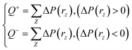
Based on the selected Cs3YSr3I12/GaN DSH, we discuss the influence of interface dipoles on charge transfer. As shown in Fig. 2a, Cs3YSr3I12/GaN DSH is a zero band-gap structure, and its projected band structure shows that the Fermi level moves across the valence band of the perovskite layer (similar to a p-type ohmic contact), which indicates the formation of III-type energy bands. With the appearance of semi-metallic properties, we speculate that the tunneling effect is likely to occur at the interface. Hence, there is no potential barrier to hinder the electron injection from Cs3YSr3I12 to GaN. The partial density of states (PDOS) shows that its CBM is mainly contributed by Y-5p, Ga-4p, I-5p and Sr-5s states, indicating that perovskite is the main contributor to the CBM of the structure. The valence band electronic structure is mainly determined by the hybridization of s-p orbitals between Y and I, and is mainly composed of I-5p and Ga-4p states, which constitutes the overall structural skeleton of the heterojunction and is the core element to form the valence band top and chemical bond. Owing to the nonlocalized nature of s and p orbitals, the large band dispersion of Cs3YSr3I12 contributes to obtaining high carrier mobility. In addition, the 2s electron of N is located at the deep level, which has little effect on the bonding and conductivity of the material, indicating that Ga in the GaN semiconductor plays an important role in adjusting the energy band width and electronic properties of the material. On the other hand, it is found in Fig. 2b that the synergistic effect of charge transfer and redistribution gives rise to the interfacial electrical dipole in the Cs3YSr3I12/GaN DSH. The localized electric field induced by the interfacial dipole not only reaches the interior of GaN to realize the overall band offset, but also the generation of reverse electric fields limits charge transfer. The dipole moment calculated by averaging the dipole charge (Fig. 2b) can be used to describe the limiting effect of the reverse electric field on charge transfer. The average positive and negative dipole charge Q± and average dipole length dz of the interface were analyzed. The formula is as follows:46| |
 | (4) |
where ZBa and Zsurface represent the positions of the Y atom and the H-GaN surface along the Z-axis, respectively. The calculation formula of the dipole moment Pz is:
 |
| | Fig. 2 (a) The projected band structure and PDOS of the Cs3YSr3I12/GaN heterostructure. The purple and red lines in the band structure denote the contribution of GaN and Cs3YSr3I12, respectively. (b) The average dipole charge and local charge density. (c) Charge-density distributions of band-edge states of the Cs3YSr3I12/GaN heterojunction. The charge-density distributions contributed by GaN and Cs3YSr3I12 are colored by purple and red, respectively. The inset indicates the schematic diagram of the dipole model during Y activation on the H-GaN surface. | |
The dipole moment of the perovskite heterojunction is 3.3 e·Å (>2 e·Å). Generally speaking, a large dipole moment will limit electron transfer, but interestingly, the edge charge in Fig. 2c indicates that electrons overflow near GaN. This apparent contradiction is resolved by considering the negative electron affinity (NEA) effect induced by the strong dipole moment.47 NEA originates from the formation of the Cs/GaN interface, and the dipole moment produced by Y element doping enhances the generation of NEA. The electron affinity χ of the heterostructure can be achieved by the following relation:
where
Ec and
Evac are the energies of the CBM and vacuum level, respectively. We compared the
χ of eight different doping elements (Table S5). The calculated
χ of Cs
3YSr
3I
12/GaN is −2.47 eV proving the existence of NEA. By comparing the average electrostatic potential (Fig. S8) and interface electron affinity of different termination planes (Table S6), we found that the Y-terminal interface produces the largest downward vacuum energy level shift (strongest interface dipole), indicating that the NEA of the Cs
3YSr
3I
12/GaN structure originates from specific Y-induced interface dipoles and charge redistribution. The existence of the NEA effect enables electrons to spontaneously migrate, effectively solving the adverse effect of dipole moment on electron transfer.
In order to further investigate adsorbates and defects, we conducted additional tests by introducing a molecule of H2O or O2 on the exposed surface and introducing representative iodine vacancy defects near the surface (Fig. S9). Although these perturbations may alter the local dipole and reduce the magnitude of χ, the interface still retains a negative electron affinity and preserves the key conclusion of spontaneous electron injection/low barrier in the Ga-terminated Y configuration. Therefore, maintaining NEA in experiments would benefit from interface passivation and device encapsulation.
3.3. Negative work function and tunnelling barrier of the Cs3YSr3I12/GaN DSH
The potential barrier is another important reason for limiting charge transfer at heterojunction contact interfaces. Among them, the work function is an important parameter, describing the energy of an electron needed to emit into vacuum. The work function WF can be achieved from the following:48where Evac and Ef are the energies of the vacuum level and Fermi level, respectively. Surprisingly, we observed that the vacuum energy level of Cs3YSr3I12/GaN is below the CBM and the calculated Φ is −1.17 eV, demonstrating the spontaneous migration of electrons (Fig. 3a).
 |
| | Fig. 3 (a) Electrostatic potential distribution and (b) carrier tunneling probability of the 2D Cs3YSr3I12/GaN DSH. The Fermi level, vacuum level and CBM are indicated by blue, red and green lines in electrostatic potential distributions, respectively. | |
The tunnelling barrier is characterized by two parameters: the height (ΦTB) and width (WTB) of the barrier. The ΦTB and WTB of the tunneling barrier can be obtained from the electrostatic potential of the Cs3YSr3I12/GaN DSH (Fig. 3a), where the potential difference between the vdW gap (Φgap) and the potential energy of 2D Cs3YSr3I12 (Φperovskite) is characterized by ΦTB. Compared with other doped perovskites (Fig. S10), the tunneling barrier of the Cs3YSr3I12/GaN DSH is the lowest (0.74 eV). In addition, tunneling barriers can also be evaluated from tunneling probability (PTB), which can be calculated as:49
| |
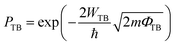 | (9) |
where ℏ is the reduced Planck constant,
m is the mass of a free electron, and
ΦTB and
WTB are the tunneling barrier height and width, respectively. The calculated
ΦTB and
WTB are 2.44 eV and 0.63 Å, respectively. Based on
eqn (9), the
PTB of the Cs
3YSr
3I
12/GaN DSH can be estimated to be 97.1%. Similarly, the
PTB of other DSHs has been predicted to span a broad range from 46.3% to 97.1% (
Fig. 3b). However, the
PTB value of the Cs
3YSr
3I
12/GaN DSH is not the highest, and the application of a DSH in electronic and optoelectronic devices requires it to have both high
PTB and weak FLP, which requires us to find a DSH that balances the influencing factors of the two.
3.4. FLP effect and conductivity of the Cs3YSr3I12/GaN DSH
Under ideal conditions, the Schottky–Mott rule can predict the strength of FLP. But the Schottky–Mott rule often cannot offer a reasonable prediction of semiconductor heterojunctions in an experiment due to strong FLP at the DSH interfaces. The FLP strength for a given semiconductor can be described by the barrier pinning factor S as follows:50,51| |
 | (10) |
where Φ denotes the interface barrier height, and Wperovskite is the work function of the 2D doped perovskite. The S is obtained by calculating the changes in interfacial potential barriers (i.e. the work function difference between the metal and semiconductor) in different metal doped perovskite heterostructures. S = 1 means that the Schottky–Mott limit is achieved, and S = 0 denotes strong FLP at the DSH interface.52 For semiconducting heterojunctions, the absolute S value lies between 0 and 1. The calculated S of the Cs3YSr3I12/GaN DSH is 0.74 (Fig. 4a), which is closer to the Schottky–Mott limit compared to values of 0.27 for Si and 0.07 for GaAs from some typical previous studies,53,54 indicating that FLP is effectively suppressed. On the basis of the calculated PTB and S values (Fig. 4b), the Cs3YSr3I12/GaN DSH satisfies both high PTB and weak FLP and is more suitable for electronic and optoelectronic applications.
 |
| | Fig. 4 (a) Relative Φ of the 2D perovskite/GaN heterostructure versus the work function values of the 2D doped perovskite. S presents the pinning factor. (b) Carrier tunneling probability PTB versus the pinning factor S in Cs3[M2]Sr3I12/GaN (M2 = Sc, Al, Y, Ln, Tl, La, Bi, Ga). (c) Electronic conductivity of the Cs3YSr3I12/GaN DSH. (d) The process of zero barrier contact transformation. | |
In addition to the PTB and FLP strength, the electronic conductivity is also an important parameter to evaluate the charge transport efficiency of DSHs.55 The electronic conductivity calculated through VASPKIT needs to be multiplied with the relaxation time (τ). By utilizing the deformation potential (DP) theory, in combination with the effective mass approximation, the τ can be calculated as:56
| |
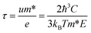 | (11) |
and
where
C is the elastic constant,
e is the deformation potential energy,
m* is the effective mass,
u is the mobility of carriers, including electrons and holes, ℏ is the reduced Planck constant,
T is the temperature,
E is the total energy of the system. Δ
a is the change of the lattice constant, Δ
a/
a0 is the magnitude of the uniaxial stress, and
S0 is the bottom area of the two-dimensional material.
Our measurements revealed a high conductivity of 7.96 × 10³ S cm−1 for the Cs3YSr3I12/GaN DSH (Fig. 4c), significantly surpassing the values reported in previous research.57–59 The Seebeck coefficient, electronic thermal conductivity, and power factor of the Cs3YSr3I12/GaN DSH are shown in Fig. S11. Compared to traditional semiconductors, GaN heterojunctions exhibit small tunneling barriers, weak pinning, zero potential barriers, and high electron transfer efficiency (Fig. 4d). Hence, the 2D Cs3YSr3I12/GaN DSH shows great potential for high performance as an electron transport layer.
4. Conclusions
In summary, guided by DFT calculations, this work systematically investigates the potential barriers and FLP effects in a series of vdW-stacked DSHs composed of monolayer GaN and a lead-free perovskite. The stability and environmental compatibility of the Cs3YSr3I12/GaN DSH are ensured through surface passivation by trivalent elements and isovalent doping of strontium (Sr). We demonstrate that coupling monolayer GaN with a Y-doped two-dimensional perovskite induces a negative work function, leading to a transition to zero barrier height. This contact transition is mainly due to the vdW interaction between the two materials at the interface, which will rearrange the charge distribution in the interface region. This charge rearrangement will change the local electrostatic potential, thereby causing the vacuum energy level to shift downward at the interface. Moreover, the formation of the Y–Ga interface facilitates the NEA effect, which significantly mitigates the adverse impacts of FLP and interface dipole moments on interlayer electron transport. Among all configurations evaluated, the Ga-top Cs3YSr3I12/GaN DSH exhibits superior performance, achieving remarkable tunneling efficiency and high electrical conductivity. This study proposes a novel strategy to overcome electron transport bottlenecks in conventional semiconductor junctions and offers promising avenues for enhancing the performance of next-generation electronic nanodevices.
Conflicts of interest
The authors declare no competing financial interest.
Data availability
The data that support the findings of this study are available from the corresponding author upon reasonable request.
Supplementary information (SI): comparison of different calculation methods, electronic properties of the Cs3[M2]Sr3I12/GaN structure (M2 = Sc, Al, Y, Ln, Tl, La, Bi, Ga), and computational details of the elastic constant. See DOI: https://doi.org/10.1039/d6ta00035e.
Acknowledgements
This research was supported by the Startup Funds for New Faculty at Southeast University (Grant No. 4007022322) and the Big Data Computing Center of Southeast University.
References
- Q. Zhang, M. Li, L. Li, D. Geng, W. Chen and W. Hu, Recent progress in emerging two-dimensional organic–inorganic van der Waals heterojunctions, Chem. Soc. Rev., 2024, 53, 3096–3133 RSC.
- Y. J. Du, J. Yang, Z. Lv, Y. Zhai, Z. Yi, Y. Xie, M. L. Zheng, X. Ma, G. Gong, Y. Wang, Y. Zhou and S. T. Han, Integration of perovskite/low-dimensional material heterostructures for optoelectronics and artificial visual systems, Adv. Funct. Mater., 2025, 2500953 CrossRef CAS.
- H. Wang, S. Li, X. Liu, Z. Shi, X. Fang and J. He, Low-dimensional metal halide perovskite photodetectors, Adv. Mater., 2021, 33, 2003309 CrossRef CAS PubMed.
- H. Dong, C. Ran, W. Gao, M. Li, Y. Xia and W. Huang, Metal halide perovskite for next-generation optoelectronics: progresses and prospects, ELight, 2023, 3, 3 CrossRef.
- J. S. Manser, J. A. Christians and P. V. Kamat, Intriguing optoelectronic properties of metal halide perovskites, Chem. Rev., 2016, 116, 12956–13008 Search PubMed.
- G. Kakavelakis, M. Gedda, A. Panagiotopoulos, E. Kymakis, T. D. Anthopoulos and K. Petridis, Metal halide perovskites for high-energy radiation detection, Adv. Sci., 2020, 7, 2002098 CrossRef CAS PubMed.
- L. Zhang, C. Sun, T. He, Y. Jiang, J. Wei, Y. Huang and M. Yuan, High-performance quasi-2D perovskite light-emitting diodes: from materials to devices, Light:Sci. Appl., 2021, 10, 61 Search PubMed.
- R. Lin, Y. Wang, Q. Lu, B. Tang, J. Li, H. Gao, Y. Gao, H. Li, C. Ding, J. Wen, P. Wu, C. Liu, S. Zhao, K. Xiao, Z. Liu, C. Ma, Y. Deng, L. Li, F. Fan and H. Tan, All-perovskite tandem solar cells with 3D/3D bilayer perovskite heterojunction, Nature, 2023, 620, 1–3 CrossRef PubMed.
- Y. Wang, Y. Zha, C. Bao, F. Hu, Y. Di, C. Liu, F. Xiang, X. Xu, X. Wen, Z. Gan and B. Jia, Monolithic 2D perovskites enabled artificial photonic synapses for neuromorphic vision sensors, Adv. Mater., 2024, 36, 2311524 Search PubMed.
- X. Zhang, Y. Zhang, H. Yu, H. Zhao, Z. Cao, Z. Zhang and Y. Zhang, Van der Waals-interface-dominated all-2D electronics, Adv. Mater., 2023, 35, 2207966 CrossRef CAS PubMed.
- X. Jiang, S. Qin, L. Meng, G. He, J. Zhang, Y. Wang, Y. Zhu, T. Zou, Y. Gong, Z. Chen, G. Sun, M. Liu, M. Li, X. Li, F. Lang and Y. Li, Isomeric diammonium passivation for perovskite-organic tandem solar cells, Nature, 2024, 635, 860–866 Search PubMed.
- Q. Zhou, C. Cai, Q. Xiong, Z. Zhang, J. Xu, L. Liang, S. Wang, W. Sun, Z. Yuan and P. Cao, Surface polarity regulation by relieving fermi-level pinning with naphthalocyanine tetraimides toward efficient perovskite solar cells with improved photostability, Adv. Energy Mater., 2022, 12, 2201243 CrossRef CAS.
- L. Yang, P. Hou, B. Wang, C. Dall'Agnese, Y. Dall'Agnese, G. Chen, Y. Gogotsi, X. Meng and X. F. Wang, Performance improvement of dye-sensitized double perovskite solar cells by adding Ti3C2Tx MXene, Chem.–Eng. J., 2022, 446, 136963 CrossRef CAS.
- J. Shi, Y. Li, Y. Li, H. Wu, Y. Luo, D. Li and Q. Meng, Eliminating the electric field response in a perovskite heterojunction solar cell to improve operational stability, Sci. Bull., 2021, 66, 536–544 CrossRef CAS PubMed.
- X. Liu, M. S. Choi, E. Hwang, W. J. Yoo and J. Sun, Fermi level pinning dependent 2D semiconductor devices: challenges and prospects, Adv. Mater., 2022, 34, 2108425 CrossRef CAS PubMed.
- P. Fu, B. Wang, M. Liu, G. Ge, J. Hou and X. Yang, Weak Fermi level pinning and low barrier interfacial contact: 2D lead-free perovskites on multilayer GaN, J. Mater. Chem. C, 2025, 13, 137–145 RSC.
- A. Z. Chen, M. Shiu, J. H. Ma, M. R. Alpert, D. Zhang, B. J. Foley, D. Smilgies, A. Lee and J. J. Choi, Origin of vertical orientation in two-dimensional metal halide perovskites and its effect on photovoltaic performance, Nat. Commun., 2018, 9, 1336 Search PubMed.
- R. K. Ulaganathan, P. K. Roy, S. M. Mhatre, R. C. Murugesan, W. Chen, M. Lai, A. Subramanian, C. Lin, Y. Chang, A. Canulescu, A. Rozhin, C. Liang and R. Sankar, High-performance photodetector and angular-dependent random lasing from long-chain organic diammonium sandwiched 2D hybrid perovskite non-linear optical single crystal, Adv. Funct. Mater., 2023, 33, 2214078 CrossRef CAS.
- Q. Han, J. Wang, S. Tian, S. Hu, X. Wu, R. Bai, H. Zhao, D. W. Zhang, Q. Sun and Li Ji, Inorganic perovskite-based active multifunctional integrated photonic devices, Nat. Commun., 2024, 15, 1536 Search PubMed.
- Y. Chen, Y. Wang, Z. Wang, Y. Gu, X. Chai, J. Ye, Y. Chen, R. Xie, Y. Zhou, Z. Hu, Q. Li, L. Zhang, F. Wang, P. Wang, J. Miao, J. Wang, X. Chen, W. Lu, P. Zhou and W. Hu, Unipolar barrier photodetectors based on van der Waals heterostructures, Nat. Electron., 2021, 4, 357–363 CrossRef CAS.
- A. Voskoboynikov, S. S. Liu and C. P. Lee, Spin-dependent tunneling in double-barrier semiconductor heterostructures, Phys. Rev. B: Condens. Matter Mater. Phys., 1999, 59, 12514 Search PubMed.
- T. Wang, W. Deng, J. Cao and F. Yan, Recent progress on heterojunction engineering in perovskite solar cells, Adv. Energy Mater., 2023, 13, 2201436 Search PubMed.
- T. Shen, J. C. Ren, X. Liu, S. Li and W. Liu, Van der Waals stacking induced transition from Schottky to Ohmic contacts: 2D metals on multilayer InSe, J. Am. Chem. Soc., 2019, 141, 3110–3115 Search PubMed.
- J. Chen, Y. H. Lou and Z. K. Wang, Characterizing spatial and energetic distributions of trap states toward highly efficient perovskite photovoltaics, Small, 2023, 19, 2305064 Search PubMed.
- Y. Zhang, K. Shinokita, K. Watanabe, T. Taniguchi, M. Goto, D. Kan, Y. Shimakawa, Y. Moritomo, T. Nishihara, Y. Miyauchi and K. Matsuda, Controllable magnetic proximity effect and charge transfer in 2D semiconductor and double-layered perovskite manganese oxide van der Waals heterostructure, Adv. Mater., 2020, 32, 2003501 Search PubMed.
- H. Xiang, J. Zhang, K. Zhao, H. Zhang, F. Ren, Y. Jia and C. Liu, Self-selective passivation of diversely charged SnO2/CsPbI3 heterointerfaces using binary ionic compounds, J. Mater. Chem. A, 2023, 11, 16395–16402 RSC.
- Y. Ma, J. Gong, P. Zeng and M. Liu, Recent progress in interfacial dipole engineering for perovskite solar cells, Nano-Micro Lett., 2023, 15, 173 Search PubMed.
- J. van der Weide, Z. Zhang, P. K. Baumann, M. G. Wensell, J. Bernholc and R. J. Nemanich, Negative-electron-affinity effects on the diamond (100) surface, Phys. Rev. B: Condens. Matter Mater. Phys., 1994, 50, 5803 CrossRef CAS PubMed.
- X. Yang, H. Shu, X. Wang, Y. Shen, N. Shen, B. Wang, J. Wan and G. Wang, Negative electron affinity driven broadband absorption of Cs3+nPbnSb2I9+3n/GaN van der Waals heterostructures, J. Mater. Chem. A, 2019, 7, 22346–22352 Search PubMed.
- X. Wang, Y. Zhang, H. Yu and J. Wu, [GaN[Mg]-Cs]:[O-Cs] model for the negative electron affinity GaN (0001) surface, Optik, 2016, 127, 7611–7624 CrossRef CAS.
- S. Kajal, G. H. Kim, C. W. Myung, Y. S. Shin, J. Kim, J. Jeong, A. Jana, J. Y. Kim and K. S. Kim, A thermally stable, barium-stabilized α-CsPbI3 perovskite for optoelectronic devices, J. Mater. Chem. A, 2019, 7, 21740–21746 RSC.
- Z. Yu, X. Chen, S. P. Harvey, Z. Ni, B. Chen, S. Chen, C. Yao, X. Xiao, S. Xu, G. Yang, Y. Yan and J. J. Berry, Gradient Doping in Sn-Pb perovskites by barium ions for efficient single-junction and tandem solar cells, Adv. Mater., 2022, 34, 2110351 CrossRef CAS PubMed.
- Y. Pan, T. Jian, P. Gu, Y. Song, Q. Wang, B. Han, Y. Ran, Z. Pan, Y. Li, W. Xu, P. Gao, C. Zhang, J. He, X. Xu and Y. Ye, Precise p-type and n-type doping of two-dimensional semiconductors for monolithic integrated circuits, Nat. Commun., 2024, 15, 9631 CrossRef CAS PubMed.
- G. Murtaza and I. Ahmad, First principle study of the structural and optoelectronic properties of cubic perovskites CsPbM3 (M = Cl, Br, I), Phys. B, 2011, 406, 3222–3229 CrossRef CAS.
- S. Saib and N. Bouarissa, Structural phase transformations of GaN and InN under high pressure, Phys. B, 2007, 387, 377–382 CrossRef CAS.
- S. Yu, D. Yoon, Y. Lee, H. Yoon, H. Han, N. Kim, C. J. Kim, K. Ihm, T. S. Oh and J. Son, Metal nanoparticle exsolution on a perovskite stannate support with high electrical conductivity, Nano Lett., 2020, 20, 3538–3544 CrossRef CAS PubMed.
- P. E. Blöchl, Projector augmented-wave method, Phys. Rev. B: Condens. Matter Mater. Phys., 1994, 50, 17953 Search PubMed.
- P. A. Korzhavyi, I. A. Abrikosov and B. Johansson, First-principles calculations of the vacancy formation energy in transition and noble metals, Phys. Rev. B: Condens. Matter Mater. Phys., 1999, 59, 11693 CrossRef CAS.
- J. Hostas and J. Rezac, Accurate DFT-D3 calculations in a small basis set, J. Chem. Theory Comput., 2017, 13, 3575–3585 CrossRef CAS PubMed.
- R. Peverati and D. G. Truhlar, Improving the accuracy of hybrid meta-GGA density functionals by range separation, J. Phys. Chem. Lett., 2011, 2, 2810–2817 CrossRef CAS.
- C. Duan, D. Hook, Y. Chen, J. Tong and R. O'Hayre, Zr and Y co-doped perovskite as a stable, high performance cathode for solid oxide fuel cells operating below 500 °C, Energy Environ. Sci., 2017, 10, 176–182 RSC.
- H. Geng, X. Zou, Y. Min, Y. Bu and Q. Lu, Advances and challenges in perovskite oxide design for high-performance zinc-air batteries: integrating experimental strategies and machine learning, Adv. Funct. Mater., 2025, 2500657 CrossRef CAS.
- R. Wang, J. Zhao, J. Ma, C. Lu, Z. Yu, G. Tu and J. Zhang, Yttrium cation doping and phenylphosphonic acid passivation for pure-red perovskite light-emitting diodes, ACS Energy Lett., 2024, 9, 4699–4707 Search PubMed.
- C. Frasca, P. Alippi, R. Schwiddessen, K. Prashanthan, G. Nasti, S. Zuo, M. O. U. Rehman, M. H. Aldamasy, N. T. P. Hartono, A. Musiienko and A. Abate, Mitigation of self-p-doping and off-centering effect in tin perovskite via strontium doping, ACS Energy Lett., 2024, 10, 526–533 Search PubMed.
- J. Gao, Q. Liu, C. Jiang, D. Fan, M. Zhang, F. Liu and B. Tang, The mechanical stability criterion of 7 large crystal system and its application: taking SiO2 as an example, Chin. J. High Press. Phys., 2022, 36, 051101 Search PubMed.
- Y. Yang, C. Liu, Y. Ding, Z. Arain, S. Wang, X. Liu, T. Hayat, A. Alsaedi and S. Dai, Eliminating charge accumulation via interfacial dipole for efficient and stable perovskite solar cells, ACS Appl. Mater. Interfaces, 2019, 11, 34964–34972 CrossRef CAS PubMed.
- N. Priel, A. Fieguth, C. P. Blakemore, E. Hough, A. Kawasaki, D. Martin, G. Venugopalan and G. Gratta, Dipole moment background measurement and suppression for levitated charge sensors, Sci. Adv., 2022, 8, 2361 CrossRef PubMed.
- M. Eyckeler, W. Mönch, T. U. Kampen, R. Dimitrov, O. Ambacher and M. Stulzmann, Negative electron affinity of cesiated p-GaN [0001] surfaces, J. Vac. Sci. Technol. B, 1998, 16, 2224–2228 Search PubMed.
- H. Qu, S. Guo, W. Zhou, Z. Wu, J. Cao, Z. Li, H. Zeng and S. Zhang, Enhanced interband tunneling in two-dimensional tunneling transistors through anisotropic energy dispersion, Phys. Rev. B, 2022, 105, 075413 CrossRef CAS.
- D. Liu, Z. Liu, J. Zhu and M. Zhang, Hydrogen-bonding enables two-dimensional metal/semiconductor tunable contacts approaching the quantum limit and the modified Schottky–Mott limit simultaneously, Mater. Horiz., 2023, 10, 5621–5632 RSC.
- W. Tan, Y. F. Lang, Y. X. Li, Y. Q. Zhao and Y. S. Ang, Designing the weak Fermi pinning and p-type Ohmic contacts to monolayer halide perovskite Cs3Bi2I9, Appl. Phys. Lett., 2025, 6, 126 Search PubMed.
- K. Murali, M. Dandu, K. Watanabe, T. Taniguchi and K. Majumdar, Accurate extraction of Schottky barrier height and universality of Fermi level de-pinning of van der Waals contacts, Adv. Funct. Mater., 2021, 31, 2010513 Search PubMed.
- S. M. Sze and K. K. Ng, Physics of Semiconductor Devices, Wiley, Hoboken, 2006 Search PubMed.
- W. A. Saidi, Influence of strain and metal thickness on metal-MoS2 contacts, J. Chem. Phys., 2014, 141, 094707 Search PubMed.
- S. Park, T. Schultz, D. Shin, N. Mutz, A. Aljarb, H. S. Kang, C. Lee, L. Li, X. Xu, V. Tung, E. J. W. List-Kratochvil, S. Blumstengel, P. Amsalem and N. Koch, The Schottky–Mott rule expanded for two-dimensional semiconductors: Influence of substrate dielectric screening, ACS Nano, 2021, 15, 14794–14803 Search PubMed.
- N. Chen, D. Luo, P. Chen, S. Li, J. Hu, D. Wang, R. Zhu and Z. Lu, Universal band alignment rule for perovskite/organic heterojunction interfaces, ACS Energy Lett., 2023, 8, 1313–1321 Search PubMed.
- X. Zhang, L. Feng, S. Zhong, Y. Ye, H. Pan, P. Liu, X. Zheng, H. Li, M. Qu and X. Wang, Schottky barrier heights and mechanism of charge transfer at metal–Bi2OS2 interfaces, Sci. China Mater., 2023, 66, 811–818 Search PubMed.
- Y. Teraoka, H. M. Zhang, K. Okamoto and N. Yamazoe, Mixed ionic-electronic conductivity of La1−xSrxCo1−yFeyO3−δ perovskite-type oxides, Mater. Res. Bull., 1988, 23, 51–58 Search PubMed.
- M. Li, H. Niu, J. E. Druce, H. Téllez, T. Ishihara, J. A. Kilner, H. Gasparyan, M. J. Pitcher, w. Xu, J. F. Shin, L. M. Daniels, L. A. H. Jones, V. R. Dhanak, D. Hu, M. Zanella, J. B. Claridge and M. J. Rosseinsky, A CO2-tolerant perovskite oxide with high oxide ion and electronic conductivity, Adv. Mater., 2020, 32, 1905200 Search PubMed.
|
| This journal is © The Royal Society of Chemistry 2026 |
Click here to see how this site uses Cookies. View our privacy policy here. 
 Open Access Article
 This Open Access Article is licensed under a Creative Commons Attribution-Non Commercial 3.0 Unported Licence
 *
*


