
 Open Access Article
 This Open Access Article is licensed under a
 Creative Commons Attribution 3.0 Unported Licence
Performance evolution of CsPbI2Br perovskite solar cells under space-equivalent stressors
Sahil Verma and
Lethy Krishnan Jagadamma*
and
Lethy Krishnan Jagadamma*
Energy Harvesting Research Group, School of Physics & Astronomy, SUPA, University of St Andrews, North Haugh, St Andrews, Fife KY16 9SS, UK. E-mail: lkj2@st-andrews.ac.uk
First published on 11th May 2026
Abstract
This study investigates the suitability of all-inorganic halide perovskites of CsPbI2Br for space applications with an emphasis on their thermal stability under the simulated Low Earth Orbit (LEO) space conditions. The substrate pre-heating is found to play a critical role in obtaining ambient stable CsPbI2Br perovskite solar cells. The in situ photovoltaic properties of the CsPbI2Br solar cells over a broad temperature range (+150 °C to −150 °C) and under combined stressors such as heat, vacuum, and AM0-like illumination were systematically investigated for both glass/ITO and fused silica/ITO substrates. The extent of performance loss and recovery is found to be strongly determined by the choice of substrates, with the fused silica/ITO-based devices showing relatively better performance recovery than the glass/ITO-based devices, after 24 h. Microstructural analysis of partial device heterostructures shows that CsPbI2Br films on fused silica retain their crystalline phase, preferred orientation, and optical absorption even under extreme temperature fluctuations, indicating better thermal compatibility. Overall, this study highlights the significance of substrate engineering in enhancing the durability of CsPbI2Br perovskite solar cells for space applications.
1. Introduction
The growing demand for sustainable and efficient energy sources has driven significant advances in photovoltaic (PV) technologies, both for terrestrial use and increasingly for aerospace applications. The rapid growth of satellite technology, tiny satellites and CubeSats has created a pressing need for lightweight, cost-effective, and highly efficient solar power solutions that can withstand the extreme conditions of space.1,2 While traditional space-grade solar cells based on crystalline silicon and gallium arsenide (GaAs) remain the standard due to their high-power conversion efficiency (PCE) and established durability, these technologies have some limitations: high fabrication costs, rigidity and substantial weight, resulting in a specific power (power to weight ratio) of 0.5–1.0 W g−1.3 These drawbacks increasingly conflict with the developing design priorities of modern space missions, which focus on miniaturisation, cost reduction, and flexible form factors.Thin-film photovoltaic technologies, mainly organic photovoltaics (OPVs), have gained attention in this regard due to their lightweight nature, mechanical flexibility, and low-temperature processing. However, OPVs exhibit poor thermal and photostability when subjected to harsh space environments, which include ultraviolet (UV) radiation, high vacuum, and wide temperature fluctuations. Subsequently, OPVs are currently unsuitable for most space applications.4,5
In this context, metal halide perovskite solar cells (PSCs) have emerged as a promising class of PV devices offering a captivating combination of high PCE, tunable optoelectronic properties, low-cost solution processability, and mechanical flexibility. In addition to their lightweight and low-cost fabrication benefits, PSCs also show an outstanding power-to-weight ratio, a significant parameter for aerospace and satellite technologies. Recent advances in perovskite photovoltaics achieving high power-to-weight benchmarks include ultra-thin perovskite cells with specific power densities of ∼50 W g−1 (ref. 6) and flexible quasi-2D cells with ∼44 W g−1.7
This exceptional power-to-weight performance not only outshines many standard photovoltaic technologies, such as crystalline silicon (∼0.2–0.3 W g−1) and gallium arsenide-based multijunction cells (∼0.5–1.0 W g−1) but also underlines the suitability of perovskites for high-altitude and orbital systems, where payload weight is a limiting factor.3 Such ultra-light, high-efficiency designs make them favourable for integration into flexible, deployable, or curved surfaces commonly used in aerospace engineering.
Among various halide perovskites, all-inorganic compositions such as CsPbI2Br have attracted particular interest for extraterrestrial applications due to their enhanced thermal stability compared to hybrid organic–inorganic perovskites.8,9 In a recent study, Kulback et al. reported that substituting volatile organic cations with inorganic caesium ions significantly improves the material's robustness against thermal degradation and humidity exposure, which are critical factors for operation beyond Earth's atmosphere.10 Furthermore, owing to its wide bandgap, CsPbI2Br is attractive not only for single-junction space photovoltaics but also as a potential top-cell absorber in multi-junction (tandem) solar cell architectures. Such configurations enable improved utilisation of the solar spectrum and higher overall power conversion efficiencies, which are particularly desirable for satellite and space power systems.11
The CsPbI2Br perovskite, with a bandgap of approximately 1.9–2.0 eV, is especially well-suited to the AM0 solar spectrum, which characterises the solar irradiance outside the Earth's atmosphere.12 This wider bandgap enables the effective absorption of high-energy photons, which are predominant in space. The mixed-halide arrangement—combining iodide and bromide—plays a crucial role in stabilising the desired photoactive α-phase of the material, thereby limiting the structural changes typically found in iodide-based materials. In one of the research studies, Zhu et al. demonstrated that bromide incorporation in CsPbI2Br helps stabilise the perovskite in its α-phase, thereby suppressing unwanted phase transitions that occur in pure iodide systems.13 This stabilisation is primarily valued under thermal and illumination stress, allowing CsPbI2Br to hold its optoelectronic properties more effectively than many of its peers. Furthermore, the material's structural and electronic properties facilitate efficient charge transport and long carrier lifetimes, all while allowing scalable and low-temperature fabrication techniques such as spin coating or thermal evaporation. These features jointly position CsPbI2Br-based PSCs as a promising candidate for lightweight, efficient, and durable photovoltaic modules suitable for space deployment.14–16
To assess the feasibility of CsPbI2Br solar cells for space applications, it is essential to understand the specific environmental conditions they will encounter, particularly in the Low Earth Orbit (LEO) regime.17,18 In LEO, solar cells are exposed to high vacuum levels (10−4 to 10−6 mbar), intense AM0 (136.6 mW cm−2) solar illumination, and rapid temperature cycling between +120 °C and −100 °C. In addition, atomic oxygen, UV radiation, and charged particle fluxes can cause surface erosion, chemical degradation, and structural damage. These environmental variables can accelerate material degradation, jeopardising solar cells' long-term operational stability and efficiency.18–21 Although several studies have investigated the stability of perovskites under vacuum and UV exposure, a significant knowledge gap remains regarding the performance and degradation mechanisms of CsPbI2Br solar cells under LEO-like stresses. This is especially true for inorganic perovskite compositions, which offer the most potential for space applications due to their thermal stability, but have received less attention than their organic-inorganic hybrid counterparts.22–24
This study addresses a substantial gap by analysing the structural, thermal, and optoelectronic stability of CsPbI2Br-based perovskite solar cells in simulated LEO-like parameters. Our research focuses on the collective effects of high vacuum, thermal cycling, and AM0-like illumination (Fig. S1), as well as the influence of substrate selection—comparing fused silica (FS/ITO) and soda-lime glass (G/ITO) on device performance under space-grade thermal stressors. FS is selected because of its superior optical properties, thermal stability and better tolerance to harsh environmental conditions in space. Due to its exceptional attributes, FS is utilised in various space applications, including window materials for spacecraft, lenses and prisms for satellite and telescope systems, and optical fibres for high-speed, high-bandwidth data transmission in communications and sensor systems.25 We employ microstructural characterisations to probe crystalline phase evolution and orientation, alongside detailed electrical and device physics to monitor efficiency changes and Current Density–Voltage (J–V) hysteresis behaviour under controlled environmental stress. We incorporate multiple characterisations to understand how CsPbI2Br solar cells fabricated on different substrates respond to space-relevant conditions. Our findings emphasise the critical role of post-deposition thermal annealing in stabilising the CsPbI2Br perovskite phase, as well as the importance of substrate selection in preserving and recovering photovoltaic performance under LEO-like stress conditions. The thermal cycling range of +150 to −150 °C was intentionally chosen to exceed typical LEO conditions (approximately +120 to −100 °C) to provide an accelerated yet conservative assessment of device thermal robustness. According to space qualification standards such as ECSS-E-ST-20-08C, thermal cycling tests are commonly designed to extend beyond expected operational limits to account for temperature overshoots, material property uncertainties, and long-term degradation mechanisms. By applying a wider temperature window, the present study aims to probe failure modes and stability margins relevant to harsh space environments, thereby ensuring the reliability of CsPbI2Br devices under realistic and worst-case mission scenarios.26
2. Results and discussions
To achieve stable and high-quality CsPbI2Br perovskite films under ambient air conditions, we investigated the effect of substrate preheating during the fabrication process. Ambient-air processing was deliberately adopted to measure the feasibility of scalable, low-cost fabrication routes beyond controlled glovebox environments. More details on the device fabrication can be found in the experimental section.As illustrated in Fig. 1a, the films deposited without preheating at 60 °C for 10 min exhibited a weak and sloped absorption onset at 550 nm with a wider estimated bandgap of ∼2.35 eV. The absorption onset, occurring around 540–550 nm, corresponds to the CsPbBr3 perovskite, as reported in previous studies.27 This absorption edge is not as sharp as one would expect for a highly crystalline film. This behaviour indicates poor crystallinity of the non-preheated samples and likely the presence of a sub-stoichiometric or incomplete phase of CsPbI2Br. The corresponding film also displayed a light brown colour, in contrast to the dark brown appearance expected for a stoichiometric CsPbI2Br, and visible non-uniformities, as seen in the optical image inset [Fig. 1a], consistent with suboptimal nucleation and growth dynamics during film formation.
 | ||
| Fig. 1 Optical and structural characterisation of CsPbI2Br perovskite films fabricated under ambient air conditions. (a) UV-vis absorbance spectrum and optical image (inset) of a film deposited without substrate preheating, (b) absorbance spectrum and corresponding optical image of CsPbI2Br film fabricated with substrate preheating, and (c) XRD pattern of the preheated CsPbI2Br film. | ||
A significant improvement in optical and structural characteristics was observed upon introducing a 10-minute substrate preheating step at 60 °C before perovskite deposition. The preheated films (Fig. 1b) exhibited a sharper absorption edge and a reduced optical bandgap of ∼1.89 eV, indicating the formation of the perovskite phase CsPbI2Br, enhanced phase purity, and improved film morphology. The inset optical image shows a visibly smoother, dark-brown film with a sharp absorption onset around 650 nm, indicative of improved crystallisation kinetics. These findings are verified by X-ray diffraction (XRD) analysis (Fig. 1c), which shows that the preheated films at 60 °C exhibit strong and well-defined (100) and (200) diffraction peaks, characteristic of the orthorhombic CsPbI2Br perovskite phase, as reported in previous studies.28 Consistent with literature reports, pure CsPbBr3 exhibits its main perovskite (100) and (200) plane peaks at 15.45° and 29.98° (2θ), whereas CsPbI2Br shows these corresponding peaks at (14.8°, 29.65°). These systematic shifts reflect lattice expansion upon partial substitution of Br− with larger I− ions and support the assignment of the mixed-halide phase.29,30 The presence of these peaks confirms successful crystallisation and preferential orientation in the vertical direction, which is desirable for efficient charge transport. Following CsPbI2Br precursor deposition on a pre-heated substrate, all films were subjected to a two-step post-deposition annealing process at 60 °C and 250 °C for 10 minutes each to promote complete crystallisation and stabilise the photoactive α-phase.
The preheating step facilitates evaporation of solvents like DMSO, leading to better spreading of the precursor and more uniform film coverage. Preheating also accelerates solvent evaporation during spin coating, facilitating faster nucleation, improved grain uniformity, and reduced defects. Without preheating, the films exhibited secondary phases, such as CsPbBr3, indicating incomplete reactions during the early stages of film development. Later, annealing at 60 °C and 250 °C allows iodine from the precursor to diffuse into the film, transforming intermediate phases into the desirable CsPbI2Br. However, this transformation is more favourable when the film has completely nucleated, which preheating helps to guarantee. These findings align with previous studies, which have shown that substrate preheating enhances film quality by increasing crystallinity, reducing defects, and improving phase purity.31–33 Collectively, these results highlight the critical role of substrate preheating in promoting uniform nucleation and enhanced crystallinity, particularly under ambient processing conditions.
After successfully establishing a reproducible protocol for ambient-air synthesis of CsPbI2Br perovskite films, we assessed their photovoltaic performance under standard AM 1.5 G illumination. The devices were fabricated using an n–i–p architecture (Glass/ITO/SnO2/CsPbI2Br/Spiro-OMeTAD/Au), with CsPbI2Br serving as the absorber layer. This baseline characterisation step was essential before subjecting the devices to more demanding space-relevant conditions such as AM0-like spectral irradiance, vacuum, and temperature cycling. Fig. 2a shows the J–V characteristics of the champion device measured in both forward (FW) and reverse (RV) scan directions. The device shows J–V hysteresis, with improved performance in the RV scan direction. Specifically, the PCE increases from 4.92% (FW) to 5.73% (RV), primarily due to an improvement in the fill factor (FF), which rises from 51.92% to 62.15%. The open-circuit voltage (VOC) remains almost constant at 1.22 V in both directions, while the short-circuit current density (JSC) shows minor variation (−7.71 vs. −7.53 mA cm−2). Box plots from Fig. 2b–e support this trend across 31 devices, where RV-scanned devices consistently show enhanced performance in terms of PCE and FF, while VOC remain relatively stable. The relatively higher J–V hysteresis in n–i–p perovskite photovoltaic device architecture incorporating metal oxide (SnO2) and Spiro-OMeTAD as charge transport layers has been previously reported.34–36 This is particularly evident when ion migration is not deliberately suppressed through compositional engineering or interface passivation. The PCE of the CsPbI2Br devices in the present study matches that reported in previous studies where no interface engineering or compositional tuning was carried out.37,38 However, state-of-the-art CsPbX3 perovskite devices with additional fabrication steps, such as interfacial passivation, additive engineering, surface treatments, or optimised electron and hole transport layers, have achieved representative PCEs well above 10%.37,38 Moreover, the higher efficiencies reported for CsPbI2Br devices in the literature are typically achieved under conditions where the entire fabrication and measurement process was carried out inside a glovebox. The CsPbI2Br devices in the present study were fabricated and measured under ambient conditions, without deliberate humidity control or device encapsulation, to achieve structurally stable, highly reproducible devices as a controlled starting point for thermal cycling studies relevant to space applications.
 | ||
| Fig. 2 (a) Champion J–V curves of CsPbI2Br-based perovskite solar cells measured in forward (FW, black) and reverse (RV, red) scan directions under AM1.5 G illumination. (b–e) Statistical box plots from 31 devices showing variation in (b) PCE, (c) FF, (d) VOC, and (e) JSC for FW and RV scans. In these statistical box plots, the width of the box represents the range where 25% to 75% of the data points lie, the middle horizontal line indicates the median (typical) value, and the whiskers show the boundary of typical data. | ||
The thermal resilience of CsPbI2Br solar cells for space applications was tested by exposing them to a complete thermal cycle under AM0-like illumination and a vacuum level of 10−3 mbar, ranging from +150 °C to −150 °C [room temperature (RT) to +150 °C, down to −150 °C, and back to RT]. Fig. 3a shows the evolution of the photovoltaic PCE and the corresponding performance parameters VOC, JSC, and FF in the FW and RV scan directions during the 30 °C min−1 temperature ramp. Additionally, before the AM0 thermal cycling test, device performance was characterised under AM1.5 G illumination, both before and after the cycling exposure, as shown in Fig. S2, to evaluate any baseline changes and verify device stability under standard terrestrial conditions.
 | ||
| Fig. 3 Thermal cycling behaviour of CsPbI2Br-based perovskite solar cells under AM0-like illumination. (a) Evolution of photovoltaic parameters (PCE, VOC, JSC, FF) during stepwise thermal cycling from room temperature (RT) to +150 °C, then down to −150 °C, followed by recovery to RT at a ramp rate of 30 °C min−1. (b) Initial J–V curve of the device before thermal cycling, (c) final J–V characteristics after thermal cycling, showing reduced JSC and FF, indicating partial degradation, (d) EQE spectra and integrated JSC for thermally cycled and control devices, showing loss of photoresponse across the visible spectrum, (e) J–V curves of the thermally cycled device after 24 hours of recovery at RT. | ||
As shown in Fig. 3a, the RV PCE dropped sharply compared to FW PCE during the heating phase, especially as the temperature approached 150 °C. Although some recovery and constant decrease in PCE were observed during the cooling phase, more constant recovery was observed during the deep cooling and warming-up phases. The final efficiency decreased to 16% in FW and 30% lower in the RV compared to the starting value, suggesting a performance loss. The photovoltaic parameters exhibit a non-linear temperature dependence, with distinct regimes characterized by varying rates of decrease in PCE and recovery. The breakdown of the PCE drop to photovoltaic performance parameters shows that this temperature-dependent performance loss is mainly driven by a substantial reduction in FF, especially in the RV scan, which falls considerably during heating and only partially recovers upon cooling. The JSC shows a relatively stable pattern throughout, with a fall during cooling but recovery during warming up. The VOC showed moderate variation, increasing slightly at the cooling phase due to suppressed non-radiative recombination, but not fully compensating for the FF loss. As temperature rises, thermally activated ion migration and interfacial degradation can become significant and can account for the observed non-linear dependence of photovoltaic performance with temperature.39 Fig. 3(b)–(e) summarise the J–V characteristics (AM0) and EQE behaviour of the G/ITO devices before, after thermal cycling, and after 24 h recovery. Fig. 3b shows PCEs of 2.39% (FW) and 5.39% (RV) with VOC = 1.29 and 1.25 V and short-circuit current density of JSC = 6.06 mA cm−2 (FW) and 5.87 mA cm−2 (RV). After the thermal cycling (Fig. 3c), the PCEs decline to 2.0% (FW) and 3.8% (RV). This corresponds to FW and RV PCE retentions of ≈ 80% and 70%, respectively of the initial PCE, i.e., a relative drop of ≈ 20% (FW) and ≈ 30% (RV). VOC is only modestly reduced (from 1.27 V to 1.17 V, ΔVOC = 0.10 V) (FW) and 1.25 V to 1.2 V, ΔVOC = 0.05 V (RV), while JSC decreases from 6.06 to 5.71 mA cm−2 (FW) (ΔJSC = 0.35 mA cm−2) and 5.87 to 5.28 mA cm−2 (RV) (ΔJSC = 0.59 mA cm−2). The EQE spectra (Fig. 3d) show that the devices retain a broad photoresponse across the 300–650 nm range, but the integrated JSC from EQE decreases (Control: 8 mA cm−2 vs. Thermally cycled: 5.7 mA cm−2), consistent with the reduced JSC in the J–V curves. After 24 h of storage in the dark at room temperature (Fig. 3e), the thermally cycled G/ITO devices partially recover to PCEs of 2.01% (FW) and 3.85% (RV), i.e., they still retain 84.0% (FW) and 71.42% (RV) of their initial PCEs. This implies that, after thermal cycling under AM0 illumination and followed by a recovery phase of 24 hours, the G/ITO -based CsPbI2Br-based perovskite solar cells exhibit a permanent performance degradation of approximately 16–30% relative to their initial FW and RV scan PCEs.
After analysing the photovoltaic properties of the G/ITO -based devices, we fabricated CsPbI2Br devices on FS substrates, which offer superior chemical purity and an ultra-low coefficient of thermal expansion (∼0.55 × 10⁻⁶ K−1).40 The FS-based devices were characterised under AM1.5 G illumination, and the photovoltaic parameters for 20 devices are provided in Fig. 4. Notably, the champion FS device [Fig. 4a] achieved a PCE of 6.31% (reverse scan), and 4.99% under FW scan conditions, underscoring the suitability of FS as a stable and efficient substrate for CsPbI2Br solar cells under AM 1.5 G. The results in Fig. 4b–e indicate trends in VOC, JSC, and FF similar to those observed on G/ITO substrates, suggesting that the substrate does not significantly affect the intrinsic device performance under AM1.5 G illumination. Specifically, the FS-based champion device exhibited a VOC of 1.23 V, a JSC of 7.29 mA cm−2, and an FF of 69.94%, resulting in a PCE of 6.31% under RV conditions. Building on this baseline, thermal cycling measurements were performed on FS devices to investigate their stability under temperature variations, as shown in Fig. 5a.
 | ||
| Fig. 4 (a) J–V curves of the champion CsPbI2Br solar cells on FS substrates. Box plots of photovoltaic performance parameters of CsPbI2Br devices fabricated on FS substrate, measured under AM 1.5 G illumination: (b) PCE, (c) FF, (d) VOC, (e) JSC. In these statistical box plots, the width of the box represents the range where 25% to 75% of the data points lie, the middle horizontal line indicates the median (typical) value, and the whiskers show the boundary of typical data. | ||
 | ||
| Fig. 5 Thermal cycling behaviour of CsPbI2Br-based perovskite solar cells fabricated on FS substrates under AM0-like illumination. (a) Evolution of photovoltaic parameters during stepwise thermal cycling from room temperature (RT) to +150 °C, then down to −150 °C, followed by recovery to RT. (b) Initial J–V curve of the device before thermal cycling under AM0, (c) final J–V characteristics after thermal cycling, showing reduced photovoltaic performance parameters indicating partial degradation, (d) EQE spectra and integrated JSC for thermally cycled and control devices, showing relative low loss of photoresponse across the visible spectrum after thermal cycling, (e) J–V curve of the photovoltaic device after 24 hours of recovery at RT. | ||
From Fig. 5a, after the initial room temperature measurement, during the heating up phase, the devices exhibit slightly higher J–V hysteresis, which then gets minimised during the cooling phase, and thereafter the devices maintain a relatively modest but stable J–V hysteresis during the deep cooling and warming up phase. VOC exhibits a small decrease consistent during cooling and stays constant for the subsequent phase, which is attributed to reduced recombination at low temperatures. JSC remains relatively constant across the entire thermal window, while FF—though affected during heating—demonstrates significant recovery during the cooling and warming up phases. The pronounced J–V hysteresis during the heating phase is largely attributable to changes in the FF and JSC. The overall thermal cycling behaviour of the CsPbI2Br devices on FS suggests that devices on FS can better withstand mechanical and electrical stress without drastic irreversible damage.
Fig. 5b and c illustrate the J–V curves of the FS devices before and after thermal cycling, respectively, under AM0-like illumination. Although the PCE decreases during the thermal cycling, it retains 80% of its initial value in the forward scan and 56% in the reverse scan. The PCE shows a moderate reduction from 2.22% (FW) to 1.78% (FW), corresponding to a retention of ≈80%, whereas the PCE (RV) drops from 3.49% to 1.96%, leading to a retention of ≈56%. Also, the corresponding J–V curves of the thermally cycled devices show drastic S-shape behaviour, indicating charge accumulation and nonideal charge extraction at the transport layer interface.41 This behaviour may result from a transient energy level misalignment at the perovskite/transport layer interface, induced by ion accumulation driven by thermal cycling. VOC remains nearly constant, decreasing from 1.16 V (FW) to 0.91 V (FW) (ΔVOC = 0.25 V), while JSC drops from 6.08 mA cm−2 to 5.11 mA cm−2. Specifically, the integrated JSC from EQE [Fig. 5d] declines only marginally from 6.6 mA cm−2 (control) to 6.1 mA cm−2 (thermally cycled), and this drop agrees with the drop in JSC, as shown in Fig. 5(b) and (c). Fig. 5e shows the J–V curves of the thermally cycled FS devices after storage in the dark for 24 hours following the thermal treatment. In this recovery stage, the devices exhibited PCEs of 2.09% (FW) and 3.12% (RV), indicating partial restoration of performance following thermal treatment i.e., they recover 94% (FW) and 89% (RV) of their initial PCEs. This implies that, after thermal cycling under AM0-like illumination and followed by a recovery phase of 24 hours, the FS-based CsPbI2Br-based perovskite solar cells exhibit a permanent performance loss of approximately 13–10% relative to their initial FW and RV scan PCEs. A comparison with the glass-based devices implies a more pronounced recovery in the FS devices. Overall, irrespective of the substrate selection, the CsPbI2Br devices undergo a drastic and permanent loss in photovoltaic performance after thermal cycling, with promising prospects for recovery during the 24-hour dark storage period, especially for the FS-based devices.
To elucidate the temperature-dependent performance of CsPbI2Br devices, the influence of different mechanistic factors, such as the choice of substrates (glass vs. FS)/ITO and functional layer architecture, was considered. Mechanical stress resulting from the mismatched thermal expansion of different functional layers within the device can play a key role in the temperature-dependent photovoltaic performance parameter. Inorganic substrates and charge transport layers such as glass, ITO, and metal oxides typically exhibit low coefficients of thermal expansion (CTE) (see Table 1). Organic layers typically exhibit higher thermal expansion due to their flexible molecular structure. However, the exact expansion rate (CTE) for doped Spiro-OMeTAD is not well-documented, which makes it hard to measure thermal mismatch directly. To address this, the glass transition temperature (Tg) of Spiro-OMeTAD provides valuable insight into its thermomechanical behaviour. Cariello et al.42 reported that doped Spiro-OMeTAD has a Tg of about 117–125 °C. Above this point, it becomes softer and rubberier, with greater molecular movement and thermal expansion. As the device heats up from room temperature to 150 °C, both Spiro-OMeTAD and the CsPbI2Br perovskite expand more than the underlying metal oxide and glass layers. This mismatch can create dissimilar strain at the buried interfaces: a compressive strain at the SnO2/perovskite and a tensile strain at the perovskite/Spiro-MeOTAD interface.43 Thermal cycling can thus induce alternating tensile and compressive stresses that cause interfacial delamination and microcracking, leading to mechanical failures that disrupt charge transport pathways, increase series resistance, and result in FF loss and overall PCE drop.44–47 Once the device cools below Tg, Spiro-OMeTAD becomes rigid and glassy again, losing the ability to relieve built-up stress, which can exacerbate the damage. Although the gold contacts are more flexible, they can still suffer from edge peeling or wrinkling, which can adversely affect charge collection.
To gather evidence of mechanical failures of thermally cycled devices, the morphological characterisation of the top Au electrode has been carried out for the devices fabricated on both the glass and the FS substrates. The corresponding SEM images are shown in Fig. S3 (a)–(d) and (e)–(h). After thermal cycling, the relatively smooth edges of the Au electrode become more granular, with the appearance of clear cracks and less interconnection. Also, the Au electrode's fine uniform granular distribution changes to a non-uniform distribution of different and larger domain sizes. These observations on the Au electrode edges and top are mostly similar for the devices fabricated on glass and FS substrates. However, the domains are more non-uniform and larger in the case of the Au electrode on the FS substrate. This can be due to the larger CTE mismatch in FS, which leads to high elastic strain energy and accelerated grain growth to relieve the strain. These microcracks, domain growth and loss of interconnection of the Au electrodes at the edges of the pixels can cause increased series resistance, reduced shunt resistance, and poor FF, thus accounting for the observed permanent performance loss of the CsPbI2Br films on G/ITO and FS/ITO substrates. Increased series resistance of the thermally cycled devices is evident from Fig. 3(b) and (c) and 5 (b) and (c).
To further assess the substrate-dependent thermal stability of CsPbI2Br-based perovskite solar cells, we investigated the temperature coefficient of photovoltaic parameters (PCE, JSC, VOC, and FF) under heating and cooling stages: RT (≈20 °C) to 150 °C, and RT to −150 °C (Fig. S4). The changes were calculated using.

During heating (RT → 150 °C), both glass and FS-based devices exhibit a reduction in PCE, with comparable negative temperature coefficients (−4 × 10⁻³ °C−1 for glass and −3.4 × 10⁻³ °C−1 for FS), arising from small temperature-dependent variations in VOC, JSC, and FF. In contrast, during the cooling phase (RT → −150 °C), FS-based devices show a very small negative temperature coefficient (−1.1 × 10⁻⁴ °C−1), indicating that the PCE remains nearly constant following its initial reduction during heating [Fig. 5a]. Glass-based devices, however, exhibit a larger negative temperature coefficient (−6.7 × 10⁻³ °C−1), reflecting a stronger temperature dependence and partial recovery of performance at lower temperatures [Fig. 3a]. The relatively large negative temperature coefficient of PCE observed for glass substrates is primarily attributed to contributions from FF (−2.3 × 10⁻³ °C−1), JSC (−1.7 × 10⁻³ °C−1) and VOC (−9.1 × 10⁻⁴ °C−1) as given in Fig. S4.
The thermal cycling data in Fig. 3a and 5a allow a direct distinction between reversible temperature-dependent behaviour and irreversible performance loss. Glass-based devices show a RV PCE drop from 5.39% to 2.47% during heating (RT to 150 °C), followed by a partial recovery toward 3.44% during cooling to RT – (−150 °C). This recovery demonstrates that a significant portion of the heating-induced loss is reversible. However, the fact that the PCE does not fully recover to its initial value indicates that an irreversible performance loss component is also present. In contrast, FS-based devices show a PCE drop from 3.49% to 1.90% during heating (RT to 150 °C) with no recovery during cooling from RT – (−150 °C), indicating that the loss incurred is predominantly irreversible during the thermal cycling. Thus, the very small temperature coefficient of PCE for the FS devices during the cooling phase reflects an absence of recovery rather than an absence of degradation. These observations suggest that while FS substrates may resist deformation due to their lower coefficient of thermal expansion (CTE), the corresponding photovoltaic devices experience a more irreversible loss in performance during thermal cycling, whereas glass-based devices retain some degree of thermally reversible behaviour. This behaviour is also evident from the J–V curves of the corresponding devices immediately after thermal cycling experiments [Fig. 3(c) and 5(c)].
To further investigate the impact of thermal cycling on operational stability, steady state (maximum power point tracking, MPP) PCE were measured under continuous AM0-like illumination (Fig. S5). For devices on glass, thermal cycling decreases the PCE from 2.09% to 1.8%. In contrast, devices on FS substrates showed a significant stability following thermal stress, PCE just dropping from 2.40% to 2.32%.
To gain a deeper understanding of the performance disparity between CsPbI2Br devices on glass and FS substrates under space-grade thermal cycling conditions, partial heterostructures of CsPbI2Br films were fabricated on the respective substrates (G/ITO and FS/ITO), and detailed microstructural characterisations were performed. Fig. 6(a) and (b) display the XRD patterns of CsPbI2Br films deposited on glass and FS substrates, control and thermally cycled (Ramp = 30 °C min−1, AM0, vacuum). For both substrates, the XRD patterns are dominated by the (100) and (200) peaks of the CsPbI2Br perovskite phase, confirming preservation of the crystalline structure after thermal treatment.28
 | ||
| Fig. 6 Structural and optical characterisation of CsPbI2Br perovskite films deposited on different substrates before (control) and after thermal cycling (Ramp = 30 °C min−1) under AM0-like illumination and vacuum. (a) XRD patterns of CsPbI2Br films on G/ITO, (b) XRD patterns of CsPbI2Br films on ITO-coated FS substrate, (c) UV-vis absorbance spectra of glass-based samples, (d) absorbance spectra of FS-based films. Scanning electron microscopy images of the CsPbI2Br films on G/ITO (e) before thermal cycling and (f) after thermal cycling (ramp = 30 °C min−1); (g) CsPbI2Br films on FS/ITO before and (h) after thermal cycling. | ||
However, a noticeable difference is observed in the intensity of the peaks on the G/ITO substrate: the intensity of the (200) peak significantly increased after thermal cycling (red curve), indicating improved crystallinity or a possible preferred orientation along the (200) plane (Fig. 6a). This could result from thermally driven grain reorganisation or partial recrystallisation.53 Quantitatively, the intensity ratio I(200)/I(100) is markedly substrate-dependent: glass samples exhibit a high preferential growth along (200) with a ratio of 2.55 (both control and thermally cycled), whereas FS samples show no such preferred growth orientation, indicated by ratios of 0.81 (control) and 0.82 (thermally cycled). The high and persistent intensity ratio of I(200)/I(100) peaks on glass is essentially unaffected by the applied thermal cycle. By contrast, the low intensity ratio of I(200)/I(100) peaks on FS indicates marginal dominance of the (100) orientation. In short, the FS samples (Fig. 6b) exhibit only a minimal change in peak intensity or width, indicating a higher structural stability of CsPbI2Br films under identical thermal cycling conditions. A shift of the (100) peak from 14.73° to 14.70° is also observed for the thermally cycled CsPbI2Br films on G/ITO substrate compared to the control, indicating minor lattice expansion likely due to strain relaxation or halide reorganisation during thermal cycling, consistent with previous reports on mixed-halide perovskites.54 The (100) and (200) peak positions remained essentially unchanged [29.93° to 29.92° for (200)] for CsPbI2Br films on a FS substrate/ITO, indicating high structural stability, which could be due to the much lower CTE of the FS substrate causing less deformation to the CsPbI2Br films during the thermal cycling process. Overall, the α-phase structure remains intact for CsPbI2Br on both substrates, and no secondary phases are detected. In addition to these main peaks, low-intensity XRD peaks are visible at 29.2° and 30.2°, which also undergo noticeable changes after thermal cycling. For the glass substrate-based CsPbI2Br films, the peak at 29.2° seems to have evolved after thermal cycling, whereas for the CsPbI2Br films on the FS substrate, the peak at 29.2° is very weak for both controlled and thermally cycled samples. Additionally, there is a peak around 30.2° for CsPbI2Br films grown on both substrates, which undergo markedly visible changes, getting slightly broader after thermal cycling. This indicates the possible microstructural evolution of CsPbI2Br films, such as grain growth, strain relaxation and texture changes (discussed further below in the SEM section) introduced during the thermal cycling. The peak assignment at 30.2° is done with caution as ITO has a strong (222) XRD peak around this 2θ value.55
The absorbance spectra of the partial heterostructures (Glass or FS/ITO/CsPbI2Br) are shown in Fig. 6(c) and (d). In the case of glass (Fig. 6c), the thermally cycled film shows a slight reduction in absorbance across the visible spectrum compared to the control structure. This could be associated with surface or bulk degradation, leading to a lower optical density. Meanwhile, the absorbance profile of the FS sample (Fig. 6d) remains virtually unchanged in both shape and intensity, in agreement with the structural stability revealed by the XRD analysis. The bandgap also remains stable (1.89 eV), indicating that the optoelectronic properties are preserved after thermal cycling for the CsPbI2Br films on FS substrates.
The surface morphology of the control and thermally cycled CsPbI2Br films on G/ITO substrates is shown in Fig. 6(e) and (f), with higher-resolution images provided in Fig. S6. The FESEM images reveal relatively uniform perovskite grains in both cases. After thermal cycling, the films exhibit slightly more edge contrast, along with the appearance of some void-like features. However, the overall morphology remains largely unchanged, indicating that the glass-based films retain their microstructural integrity under the applied thermal stress. This behaviour is consistent with the XRD results, where the I(200)/I(100) ratio remains high (2.55), suggesting stable preferred orientation and crystallinity.
In contrast, CsPbI2Br films deposited on fused silica (FS) [Fig. 6(g) and (h)] exhibit a more pronounced morphological evolution upon thermal cycling. The control sample (Fig. 6g) shows relatively compact grains with smoother features, whereas the thermally cycled film (Fig. 6h) develops finer-scale structures and increased surface heterogeneity, along with more noticeable contrast and altered texture. This indicates that, unlike glass, FS-based films undergo microstructural rearrangement under rapid thermal cycling. Despite minimal changes in XRD peak intensity and the nearly constant I(200)/I(100) ratio (0.81–0.82), these SEM observations suggest that structural changes occur at the mesoscale that are not fully captured by bulk crystallographic analysis. This morphological evolution may account for the performance loss (and increased series and shunt resistance) observed in FS-based devices after thermal cycling (Fig. 5c). Such behaviour is consistent with previously reported temperature-dependent studies of CsPbI2Br films and related inorganic perovskites. Thermal annealing is known to induce pronounced morphological evolution, including increased surface roughness and microstructural rearrangement at elevated temperatures, driven by enhanced ionic mobility and thermally activated phase processes.56 In addition, the crystallisation dynamics of CsPbI2Br films are highly temperature-dependent, where variations in grain size and film morphology play a critical role in determining device performance.57
To understand the recombination and charge extraction properties of the photogenerated charge carriers in pristine and thermally cycled samples, light intensity-dependent J–V characteristics were measured for CsPbI2Br devices fabricated on both glass and FS substrates.
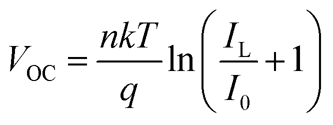
The VOC scales with light intensity [Fig. 7(a and b)] according to 58:
 | (1) |
 | ||
| Fig. 7 Light-intensity-dependent (a and b) VOC, and (c and d) JSC, for CsPbI2Br solar cells fabricated on glass (G) and FS substrates under control, thermally cycled, and recovery conditions. Transient photocurrent decay curves for CsPbI2Br solar cells fabricated on (e) glass and (f) FS substrates under control, thermally cycled, and recovery conditions. Cole–Cole plots from dark impedance measurements are shown in (g) and (h) for the respective devices, providing insight into charge transport and recombination behaviour. | ||
At high light intensity
 | (2) |
 | (3) |
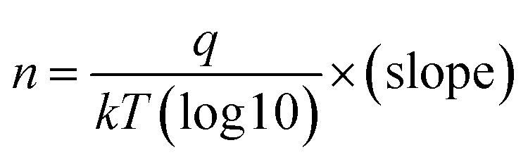
and from the slope, we can extract n,
 | (4) |
![[thin space (1/6-em)]](https://www.rsc.org/images/entities/char_2009.gif) (I) yields n, which reflects the dominant recombination mechanism.
(I) yields n, which reflects the dominant recombination mechanism.
For FS-based devices [Fig. 7(a and b)], the ideality factor, n, is 2.56 for the control, which increases to 2.95 for the thermally cycled samples and reaches 4.33 in the recovery devices. This progressive rise in ideality factor indicates the activation of non-radiative recombination pathways and potential transport limitations induced by combined light and thermal stress.59 In contrast, glass-based devices exhibit relatively stable ideality factors of around 2.2–2.4 across all conditions, which is still higher than the n = 1 for bimolecular recombination, indicating the dominance of monomolecular, trap-assisted recombination processes. In Fig. 7(c and d), the JSC shows a nearly linear dependence on light intensity for both substrates, consistent with a power law relationship JSC ∝ l α, where α–1.56 This linearity indicates minimal charge accumulation due to space charge effects in the devices.
Transient photocurrent (TPC) measurements (as shown in Fig. 7e and f) were carried out on both Glass/ITO -based and FS substrate-based devices, as these measurements can reveal carrier extraction dynamics and the effect of trapping/recombination, especially at the perovskite/transport layer interfaces. Both control and thermally cycled devices on G/ITO substrates exhibit rapid current decay (∼15 µs), indicating relatively rampant charge extraction with minimal trapping. In contrast, the device that went into recovery generates a long-lived tail, characteristic of trap-assisted recombination. This implies that the recovery process, rather than healing, yields additional trap states—likely due to interfacial strain or unfavourable interactions between the perovskite and transport layers or due to the degradation of the photoactive layer over time. These traps can slow down extraction kinetics by transiently capturing carriers and extending their lifetime in the device.
On FS substrates, the picture is flipped. The control device shows lagging extraction with continuous photocurrent tails, contemplating a high density of trap states that impede carrier transport. Thermal cycling and recovery shorten the decay, indicating reduced trapping and more efficient extraction pathways. The recovery-treated FS device exhibits the fastest kinetics, returning to baseline within ∼15 µs, consistent with trap passivation and enhanced carrier mobility. This improvement may arise from better structural relaxation and reduced interfacial defect formation when the perovskite is coupled with FS, which has different thermal expansion and surface chemistry than glass.
To corroborate the experimental observation from the TPC measurements, impedance measurements (under dark conditions) were carried out on the respective devices. Fig. 7g shows the Cole–Cole plots of the impedance spectra of the control, thermally cycled and recovery devices on G/ITO substrates. The Cole–Cole plots were fitted with the equivalent circuit shown in the inset of Fig. 7g. The Rs corresponds to the series resistance, R1 is the electronic resistance (transport resistance), C1 is the geometric capacitance, R2 is the ionic resistance, and CPE is the constant phase element and, in this case, represents the ionic capacitance.60,61
The fit parameters are given in Tables S1 and S2. For the G/ITO based devices, as shown in Table S1, the series resistance of the thermally cycled and ‘recovery stage’ devices has slightly increased compared to the control samples. Even though the geometric capacitance remains almost the same across the devices, the electronic resistance is drastically reduced for the thermally cycled sample (4.9 M Ω) compared to the control devices (7.4 M Ω). In contrast, for the recovery phase devices, the electronic resistance (11 M Ω) is even higher than that of the control devices. The low electronic or transport resistance of the thermally cycled devices can be correlated to the enhanced crystallinity of the perovskite active layer, as shown in Fig. 6a. The high electronic resistance of the recovery phase devices is consistent with the very slow charge extraction observed for the corresponding devices, as shown in the TPC measurements [Fig. 7e]. In addition to the electronic resistance changes, the ionic resistance has also drastically decreased for the thermally cycled and recovery phase devices (from 5 k Ω to 2 k Ω), with a corresponding decrease in ionic capacitance (from 15 nF to 8 nF). The decrease in ionic transport resistance and ionic capacitance implies that for the thermally cycled and recovery phase devices, the transport of ions and vacancies is favoured with a reduction in the interface charge accumulation, supporting the permanent performance degradation observed in these devices after thermal cycling.
The Cole–Cole impedance spectra analysis of the devices on FS substrates is shown in Fig. 7h. Like G/ITO based devices, the FS-based samples also exhibit a reduction in electronic or transport resistance for the thermally cycled sample (8.5 M Ω) compared to the control (24.6 M Ω). In contrast, for the recovery samples, the electronic resistance is closer to that of the control sample (Table S2). The high electronic resistance of the control devices aligns with the relatively longer charge extraction times for the corresponding devices, as revealed in the TPC measurements [Fig. 7f]. The decrease in ionic transport resistance (from 3 k Ω to 1 k Ω) and increase in ionic capacitance (from 1 nF to 50 nF) imply that for the thermally cycled and recovery phase devices, the transport of ions and vacancies is favoured, but with enhanced interface charge accumulation. The higher thermal expansion coefficient mismatch between the substrate and the different functional layers may be causing higher internal stress, damaging the transport and contact layers (as seen from Fig. S3), and hence the possible charge accumulation at the buried interfaces. Considering the relatively stable microstructure of the perovskite active layer on the FS substrate, as discussed above in the microstructural characterisation, this enhanced ionic capacitance may be due to degradation of the transport layers, specifically Spiro-MeOTAD. However, a further detailed cross-sectional layer-by-layer investigation is required to quantify the contribution of each functional layer in the observed performance degradation of G/ITO and FS/ITO-based CsPbI2Br devices due to space-grade thermal cycling process.
3. Conclusion
This study demonstrated that substrate preheating is essential for producing phase-pure, crystalline CsPbI2Br films under ambient processing conditions, enabling promising photovoltaic performance. Furthermore, our results revealed the critical influence of substrate selection on the thermal cycling stability and overall performance of CsPbI2Br perovskite solar cells under simulated space conditions. Although CsPbI2Br solar cells fabricated on both glass and FS substrates exhibit comparable photovoltaic performance under AM0-like illumination, in situ thermal cycling measurements show that, under combined stressors—thermal cycling, AM0 illumination, and vacuum—the extent of performance degradation and recovery strongly depends on the choice of substrate type.Temperature-coefficient analysis of photovoltaic performance parameters during thermal cycling enabled a clear distinction between reversible temperature-dependent behaviour and irreversible performance loss for glass vs. fused silica (FS)-based substrates. During thermal cycling, FS-based devices exhibited greater irreversible photovoltaic performance loss than those on glass, whereas the reversible performance for devices on glass was superior to that on FS substrates. Additionally, the CsPbI2Br films on FS substrates showed altered surface morphology, whereas the films on glass devices exhibited very similar morphological features before and after thermal cycling. However, after a 24 h recovery period, the FS-based devices showed enhanced performance recovery compared to the devices on the glass substrates.
Conflicts of interest
There are no conflicts to declare.Data availability
The research data supporting this publication can be accessed at https://doi.org/10.17630/4f1bba95-841b-4874-b34a-14df9e93e605.Supplementary information (SI) is available. See DOI: https://doi.org/10.1039/d5se01367d.
Acknowledgements
L. K. J. acknowledges funding from UKRI-FLF through MR/T022094/1. Both L. K. J. and S. V. acknowledge the funding from St Leonard's World-Leading PhD Scholarship.References
- Ho-Baillie and W. Y. Anita, et al., Deployment opportunities for space photovoltaics and the prospects for perovskite solar cells, Adv. Mater. Technol., 2022, 7(3), 2101059 CrossRef CAS.
- M. A. Green and Ho-B. Anita, Perovskite solar cells: the birth of a new era in photovoltaics, ACS Energy Lett., 2017, 2(4), 822–830 CrossRef CAS.
- R. Verduci, et al., Solar energy in space applications: review and technology perspectives, Adv. Energy Mater., 2022, 12(29), 2200125 CrossRef CAS.
- P. Cheng and X. Zhan, Stability of organic solar cells: challenges and strategies, Chem. Soc. Rev., 2016, 45(9), 2544–2582 RSC.
- E. K. Solak and E. Irmak, Advances in organic photovoltaic cells: a comprehensive review of materials, technologies, and performance, RSC Adv., 2023, 13(18), 12244–12269 RSC.
- C. Jia, et al., Ultra-thin perovskite solar cells with high specific power density based on colorless polyimide substrates, Nano Energy, 2024, 131, 110259 CrossRef CAS.
- B. Hailegnaw, et al., Flexible quasi-2D perovskite solar cells with high specific power and improved stability for energy-autonomous drones, Nat. Energy, 2024, 9(6), 677–690 CrossRef CAS.
- Z. Wang, et al., Formation and stabilization of inorganic halide perovskites for photovoltaics, Matter, 2021, 4(2), 528–551 CrossRef CAS.
- S. Bello, et al., An introduction to perovskites for solar cells and their characterisation, Energy Rep., 2022, 8, 89–106 CrossRef.
- M. Kulbak, et al., Cesium enhances long-term stability of lead bromide perovskite-based solar cells, J. Phys. Chem. Lett., 2016, 7(1), 167–172 CrossRef CAS PubMed.
- G. W. Yoon, et al., Perovskite tandem solar cells for low Earth orbit satellite power applications, Adv. Energy Mater., 2025, 15(2), 2400204 CrossRef CAS.
- Y. Wang, et al., Cesium lead iodide perovskites: optically active crystal phase stability to surface engineering, Micromachines, 2022, 13(8), 1318 CrossRef PubMed.
- C. Zhu, et al., Understanding the stability origins of ambient stable CsPbI 2 Br inorganic halide perovskites, J. Mater. Chem. A, 2022, 10(24), 13124–13136 RSC.
- Y. Tu, et al., Perovskite solar cells for space applications: progress and challenges, Adv. Mater., 2021, 33(21), 2006545 CrossRef CAS PubMed.
- X. Liu, et al., The progress and efficiency of CsPbI 2 Br perovskite solar cells, J. Mater. Chem. C, 2023, 11(2), 426–455 RSC.
- J. Yang, et al., Potential applications for perovskite solar cells in space, Nano Energy, 2020, 76, 105019 CrossRef CAS.
- G. Sebestyen, et al., Low Earth Orbit Satellite Design, Springer International Publishing, 2018 Search PubMed.
- A. F. Hepp, R. P. Raffaelle, and I. T. Martin. "Space photovoltaics: New technologies, environmental challenges, and missions." Photovoltaics beyond Silicon. Elsevier, 2024. 675–766 Search PubMed.
- A. L. Andrady, et al., Effects of increased solar ultraviolet radiation on materials, J. Photochem. Photobiol., B, 1998, 46(1–3), 96–103 CrossRef CAS PubMed.
- B. A. Banks, et al., Atomic oxygen effects on spacecraft materials, Ninth International Symposium on Materials in a Space Environment, No. NASA/TM-2003-212484, 2003 Search PubMed.
- A. D. Sheikh, et al., Effects of high temperature and thermal cycling on the performance of perovskite solar cells: acceleration of charge recombination and deterioration of charge extraction, ACS Appl. Mater. Interfaces, 2017, 9(40), 35018–35029 CrossRef CAS PubMed.
- R. Guo, et al., Degradation mechanisms of perovskite solar cells under vacuum and one atmosphere of nitrogen, Nat. Energy, 2021, 6(10), 977–986 CrossRef CAS.
- D. Zhang, et al., Degradation pathways in perovskite solar cells and how to meet international standards, Commun. Mater., 2022, 3(1), 58 CrossRef.
- V. Romano, et al., Advances in perovskites for photovoltaic applications in space, ACS Energy Lett., 2022, 7(8), 2490–2514 CrossRef CAS PubMed.
- L. Galuppi and G. Royer-Carfagni, Thermo-optical modelling of transparent multilayer panels for space applications in low Earth orbit, Aero. Sci. Technol., 2025, 110890 Search PubMed.
- Source: https://ecss.nl/standard/ecss-e-st-20-08c-rev-2-photovoltaic-assemblies-and-components-20-april-2023/.
- L. K. Jagadamma, et al., Nanoscale heterogeneity in CsPbBr3 and CsPbBr3: KI perovskite films revealed by cathodoluminescence hyperspectral imaging, ACS Appl. Energy Mater., 2021, 4(3), 2707–2715 CrossRef CAS.
- G. Yin, et al., Precursor engineering for all-inorganic CsPbI2Br perovskite solar cells with 14.78% efficiency, Adv. Funct. Mater., 2018, 28, 1803269 CrossRef.
- H. Chen, et al., Thermal stability of cspbbr3 perovskite quantum dots assembled with sba-15, Coatings, 2021, 11(8), 953 CrossRef CAS.
- C.-Ho Tien, et al., High-quality all-inorganic perovskite CsPbBr3 quantum dots emitter prepared by a simple purified method and applications of light-emitting diodes, Energies, 2019, 12(18), 3507 Search PubMed.
- H. Zhang, et al., Effects of substrate temperature on the crystallization process and properties of mixed-ion perovskite layers, J. Mater. Chem. A, 2019, 7(6), 2804–2811 RSC.
- K. Huang, et al., Highly Efficient Perovskite Solar Cells Processed Under Ambient Conditions Using In Situ Substrate-Heating-Assisted Deposition, Sol. RRL, 2019, 3(3), 1800318 CrossRef.
- G. Wang, et al., Optimizing the substrate pre-heating and post-annealing temperatures for fabricating high-performance carbon-based CsPbIBr2 inorganic perovskite solar cells, Electrochim. Acta, 2020, 349, 136354 CrossRef CAS.
- N. K. Elumalai and A. Uddin, Hysteresis in organic-inorganic hybrid perovskite solar cells, Sol. Energy Mater. Sol. Cells, 2016, 157, 476–509 CrossRef CAS.
- R. T. Prabu, et al., CsPbI3 perovskite solar cell and decoding its skink feature in JV curve, Mater. Sci. Semicond. Process., 2023, 162, 107539 CrossRef CAS.
- A. Bulloch, et al., Hysteresis in hybrid perovskite indoor photovoltaics, Philos. Trans. R. Soc., A, 2022, 380(2221), 20210144 CrossRef CAS PubMed.
- T. Ma, et al., The development of all-inorganic CsPbX3 perovskite solar cells, J. Mater. Sci., 2020, 55(2), 464–479 CrossRef CAS.
- C. Shen, et al., All–inorganic perovskite solar cells: defect regulation and emerging applications in extreme environments, Adv. Mater., 2024, 36(25), 2401498 CrossRef CAS PubMed.
- S. Kim, et al., Relationship between ion migration and interfacial degradation of CH3NH3PbI3 perovskite solar cells under thermal conditions, Sci. Rep., 2017, 7(1), 1200 CrossRef PubMed.
- B. Deng, Y. Shi and F. Yuan, Investigation on the structural origin of low thermal expansion coefficient of fused silica, Materialia, 2020, 12, 100752 CrossRef CAS.
- J. C. Wang, et al., Charge accumulation induced S-shape J–V curves in bilayer heterojunction organic solar cells, Org. Electron., 2011, 12(6), 880–885 CrossRef CAS.
- M. Cariello, et al., Synthesis of SOT-OH and its application as a building block for the synthesis of new dimeric and trimeric Spiro-OMeTAD materials, Mol. Syst. Des. Eng., 2022, 7(8), 899–905 RSC.
- T. Malinauskas, et al., Enhancing thermal stability and lifetime of solid-state dye-sensitized solar cells via molecular engineering of the hole-transporting material spiro-OMeTAD, ACS Appl. Mater. Interfaces, 2015, 7(21), 11107–11116 Search PubMed.
- W. Yang, et al., Toward highly thermal stable perovskite solar cells by rational design of interfacial layer, Iscience, 2019, 22, 534–543 Search PubMed.
- M. M. Tavakoli, et al., Efficient, flexible and mechanically robust perovskite solar cells on inverted nanocone plastic substrates, Nanoscale, 2016, 8(7), 4276–4283 RSC.
- M. E. Bush, et al., Space environment considerations for perovskite solar cell operations: A review, Acta Astronaut., 2025, 235, 235–250 CrossRef CAS.
- Se-Y. Jeong, H.-S. Kim and N.-G. Park, Challenges for thermally stable spiro-MeOTAD toward the market entry of highly efficient perovskite solar cells, ACS Appl. Mater. Interfaces, 2022, 14(30), 34220–34227 CrossRef CAS PubMed.
- J.-M. Lee, et al., Effect of barrier layers on the properties of indium tin oxide thin films on soda lime glass substrates, Thin Solid Films, 2009, 517(14), 4074–4077 CrossRef CAS.
- H.-S. Lee, et al., Analysis of thermo-mechanical behavior of ITO layer on PET substrate, 2011 IEEE 61st Electronic Components and Technology Conference (ECTC), IEEE, 2011 Search PubMed.
- He Zhu, et al., Twin crystal induced near zero thermal expansion in SnO2 nanowires, J. Am. Chem. Soc., 2018, 140(24), 7403–7406 CrossRef CAS PubMed.
- D.-J. Xue, et al., Regulating strain in perovskite thin films through charge-transport layers, Nat. Commun., 2020, 11(1), 1514 CrossRef CAS PubMed.
- A. I. Oliva, et al., Temperature coefficient of resistance and thermal expansion coefficient of 10-nm thick gold films, Thin Solid Films, 2017, 623, 84–89 CrossRef CAS.
- S. Qin, et al., Tuning photoelectric conversion in hybrid perovskites by thermal cycling, J. Mater. Chem. A, 2025, 13(12), 8843–8851 RSC.
- B. Yang, et al., Strain effects on halide perovskite solar cells, Chem. Soc. Rev., 2022, 51(17), 7509–7530 RSC.
- D. Raoufi and A. Taherniya, The effect of substrate temperature on the microstructural, electrical and optical properties of Sn-doped indium oxide thin films, Eur. Phys. J. Appl. Phys., 2015, 70(3), 30302 CrossRef.
- A. Papadopoulou, et al., In situ annealing effect on thermally co-evaporated CsPbI2Br thin films studied via spectroscopic ellipsometry, ACS Appl. Mater. Interfaces, 2024, 16(36), 47889–47901 CrossRef CAS PubMed.
- D. Bai, et al., Temperature-assisted crystallization for inorganic CsPbI2Br perovskite solar cells to attain high stabilized efficiency 14.81%, Nano energy, 2018, 52, 408–415 CrossRef CAS.
- S. Zeiske, et al., Light intensity dependence of the photocurrent in organic photovoltaic devices, Cell Rep. Phys. Sci., 2022, 3, 10 Search PubMed.
- N. Gasparini, et al., The role of the third component in ternary organic solar cells, Nat. Rev. Mater., 2019, 4(4), 229–242 CrossRef.
- A. Guerrero, J. Bisquert and G. Garcia-Belmonte, Impedance spectroscopy of metal halide perovskite solar cells from the perspective of equivalent circuits, Chem. Rev., 2021, 121(23), 14430–14484 CrossRef CAS PubMed.
- E. Von Hauff and D. Klotz, Impedance spectroscopy for perovskite solar cells: characterisation, analysis, and diagnosis, J. Mater. Chem. C, 2022, 10(2), 742–761 RSC.
| This journal is © The Royal Society of Chemistry 2026 |