DOI:
10.1039/D6RA00262E
(Paper)
RSC Adv., 2026,
16, 8985-9011
Performance optimization and machine learning-guided parameter sensitivity analysis of lead-free KGeCl3 perovskite solar cells
Received
10th January 2026
, Accepted 5th February 2026
First published on 13th February 2026
Abstract
This study gives a realistic insight into the effectiveness of lead-free Ge-based perovskite solar cells (PSCs) using KGeCl3 as the absorber layer in combination with four different electron transport layers (ETLs), including WS2, ZnSe, PC60BM, and SnS2, with copper iron tin sulfide (CFTS) serving as the hole transport layer (HTL). Initially, key material parameters such as layer thickness, donor density (ND), acceptor density (NA), defect density (Nt), interface defect densities (IL1 & IL2), series resistance (Rs), shunt resistance (Rsh), operating temperature (K), and back contact work function (eV) are varied using a SCAPS-1D simulator to optimize device performance. Between the four cell configurations, the FTO/CFTS/KGeCl3/WS2/Au structure has achieved the highest performance with a power conversion efficiency (PCE) of 21.39%, short-circuit current density (JSC) of 39.526 mA cm−2, fill factor (FF) of 76.56%, and open-circuit voltage (VOC) of 0.706 V at a simulated temperature of 300 K. Other configurations using ZnSe, PC60BM, and SnS2 as ETLs showed PCE values of 21.38%, 21.05%, and 20.43%, respectively. Furthermore, an integrated machine learning framework with four supervised learning methods, i.e., Random Forest, XGBoost, CatBoost, and Decision Tree, has been utilized to effectively evaluate the importance of material features. Out of the algorithms, CatBoost has the highest performance with R2 and accuracy values of 0.984 and 99.344%, respectively.
1. Introduction
With the global energy requirement and the depletion of fossil fuel reserves, as well as the deep impact of the carbon-based energy environment, research into sustainable, efficient photovoltaic (PV) technologies has become very popular.1 In the present context, perovskite solar cells (PSCs) could be considered as being among the very promising next-generation photovoltaic structures.2,3 Since their first demonstration in 2009, the power conversion efficiency (PCE) of PSCs has increased at an unprecedented rate, rising from 3.8% to over 26.1% within less than ten years, and with reports of even higher performance under optimized laboratory conditions.4 The sides of perovskite cells are evolving quickly; as a result, considerable research has been done on morphology control.5 Such rapid advances are due mostly to the exceptional optoelectronic features of perovskite materials; they can be fine-tuned, have strong absorption coefficients, long charge-carrier diffusion paths, and high electron–hole mobilities.6–9 In addition, PSCs benefit from facile, low-cost manufacture as well as compatibility with flexible substrates, all of which make them a product attractive for industrial production and scale-up.8,10
Perovskite materials have set a landmark to make a gradual improvement in advancing the PCE of PSCs.11 A diverse amount of perovskite has been developed through bandgap engineering over the last few decades.12 ABX3 contains the basic structure of perovskite that includes A, B, and X for organic inorganic cations, metal cation, and halogen ion, respectively.13 Recently, various kinds of these structures with different compositions have been promising for use as a solar absorber. It has been found that through the addition of small cations such as cesium (Cs+), methylammonium (MA+), or formamide (FA+), with halide ions, perovskite structures can be modified and have their bandgaps adjusted towards different light spectra.14–16 At present, however, the industry is faced with a shortage of raw materials and increasing demand for end-use products after so many years of pure research.10 Consequently, there is a growing need that lead-halide perovskite sensitized cells will soon appear on the market.17 But, lead-based perovskite has a major drawback because of its toxic nature for the environment.18 One of the leading candidates for replacement of both lead-free necessity and environmental concerns is germanium (Ge2+).19 Ge2+ has properties that make it much more resistant than tin (Sn2+) to oxidize and also happens to be able to exhibit suitable direct bandgaps with high absorption coefficients (∼105 cm−1) and an elevated static refractive index.20,21 Most importantly, germanium-based compounds are more friendly to the environment than their heavy metal counterparts like lead, and the element has relatively abundant natural reserves.22 Its usage happens frequently in sustainable energy applications; however, it has had a history of low performance because of the compound's migration up into Ge4+, lower defect tolerance, and sensitivity to moisture.23 On top of that, Shockley–Read–Hall (SRH) recombination is sped up and device lifetimes are shortened as a consequence.24 At the moment, potassium germanium chloride (KGeCl3) is making a name for itself as a next-generation lead-free perovskite material because of its superb optoelectronic characteristics with good stability, both thermal and mechanical.25,26 After crystallizing with K+ as the A-site, Ge2+ as the B-site, and Cl− on the third X-site into perovskite-structured ABX3 compounds, KGeCl3 has been found to have excellent thermal resistance, remaining stable and showing no decomposition at over 100 °C.27 Meanwhile, it offers greater tear strength in humid environments than organic cation-based perovskites and shows much less deterioration from UV rays.23 A past report by Roknuzzaman et al. in ref. 28 revealed that CsBX3, where B stands for Sn, Ge, and X for Cl, Br, and I-based perovskite, has more magnificent optoelectronic properties than the Pb-based perovskite for solar cell applications. Its single-junction quasi-bandgap energy is about 1.1 eV, so it lies in the optimal range for solar cells.29 It also has a strong absorption coefficient and will harvest photons efficiently within the visible spectrum. Furthermore, KGeCl3 demonstrates low rates for Auger recombination (<10−8 cm3 s−1) and high charge carrier mobilities of 60–100 cm2 V−1 s−1.30 In other words, quick charge transport with a minimum loss in energy is assured. Together with favorable band alignments with a vast variety of electron and hole transport layers, these intrinsic material properties have already led to simulated device conversion efficiencies (PCEs) of higher than 25% when the assembly of layers is optimized. A recent study by Ur Rehman et al. showed a massive improvement via numerical simulation by FTO/MoO3/KGeCl3/WS2/Au structure with PCE of 29.83% with continuous optimization of every layer.31 This advancement is possible due to selecting the efficient carrier transport layers (CTLs), including the ETL and HTL. Taken together, these attributes make KGeCl3 an environmentally friendly, structurally stable, and high-performance absorber material—a green candidate for next-generation PSCs and sustainable PV technologies.
Due to their unique optoelectronic properties and excellent energy band alignment, inorganic and organic semiconductors have been intended for use in electron transport layers (ETLs) in perovskite solar cells.32 A careful selection of the CTLs can enhance both stability and performance of solar cells. Transition metal dichalcogenides like WS2 offer high electron mobility and strong environmental stability.33 Proper band alignment between the absorber layer is one of the main motives for choosing the CTLs.34 This also ensures minimum parasitic resistance and lower recombination loss.35 With atomically thin layered structures, they provide efficient charge extraction while retaining transparency to sunlight enough for an absorbing layer made up of the perovskite crystal.36 ZnSe is a wide bandgap (≈2.7 eV) semiconductor with high transparency and chemical stability.37 The conduction band alignment with perovskites makes it an environmentally friendly, low-cost, and non-toxic ETL alternative to traditional materials such as TiO2. For this similar reason, fullerene derivatives like PC60BM can be found in many perovskite structures. They are easily processed at low temperatures, passivate the interface traps, and have a strong attraction for electrons. Those phenomena greatly reduce hysteresis and greatly improve device reproducibility.38,39 In addition, metal chalcogenides with layer structures, such as SnS2, share a high electron mobility with a wide bandgap (≈2.2 eV).40 They are nontoxic, environmentally friendly, and durable. As a result, they help ensure long-term device stability through efficient charge transport.34 Compared with conventional TiO2 and SnO2, the ETL materials WS2, ZnSe, SnS2, and PC60BM offer more favorable band alignment with KGeCl3, reduced interfacial recombination, and enhanced electron extraction.41,42 Those phenomena are maintaining high optical transparency, environmental compatibility, and efficient charge transport.43 Approaches with KGeCl3 with distinct carrier transport layers (CTLs) have made PCEs near 30%, and simulated studies showed its potential. For instance, Z. Abbasi et al.29 revealed the layout of CSTO/KGeCl3/nPB achieved 29.30% PCE with other performance parameters (VOC ≈ 0.815 V, JSC ≈ 41.8 mA cm−2, FF ≈ 85.97%), while FTO/SnS2/KGeCl3/Cu2O/C configuration achieved 15.83% PCE (VOC ≈ 0.545 V, JSC ≈ 41.91 mA cm−2, FF ≈ 69.24%) by M. A. F. Siddique et al. in 2024.26 Based on these findings, we are attempting to analyze KGeCl3 as an absorber with four efficient ETLs (WS2, ZnSe, PC60BM, SnS2) and other layers like fluorine-doped tin oxide (FTO) and CFTS. With the addition of artificial intelligence (AI) in solar technology, a new way of performance acceleration is unlocked with different machine learning (ML) approaches.44–46 Recently, Liu et al. in 2026 have proposed a deep learning-guided screening framework that accelerates the discovery of high-efficiency donor–acceptor pairs in organic photovoltaics by accurately capturing structure–property relationships. This technique is named SolarPCE-Net, and the synergistic interactions of the method demonstrate the growing impact of advanced AI architectures in PV materials discovery.47 This category of studies takes into consideration the cell's internal and external parameters for the optimization process. To further enhance device performance, many similar studies have considered the optimization of absorber thickness, doping density like donor density (ND) and acceptor density (NA), defect density (Nt), interface defects (IL1, IL2), active temperature (aided by post-deposition thermal annealing), work-function alignment, and resistive losses (series and shunt) to be examined both theoretically and practically.27,48–50
In our proposed numerical modeling, lead-free KGeCl3 has been utilized as an absorber layer with four different ETLs (ZnSe, WS2, PC60BM, SnS2) and CFTS as an HTL layer. Those materials were selected for their excellent PV performance, high extraction capacity, and lower recombination as per previous studies. The KGeCl3 appears to have thermal and chemical stability, high PCE, proper mobility of electrons and holes, along with tunable bandgaps (1.1 eV), which increases the lifespan of the solar cell.25,26,51 Furthermore, we analyze the impact of different parameters such as thickness, ND, NA, Nt, interface defect density (IL1 & IL2), temperature, work function, series and shunt resistance with the help of solar cell capacitance simulator (SCAPS-1D). Additionally, four supervised machine learning techniques, i.e., random forest (RF), extreme gradient boosting (XGBoost), categorical boosting (CatBoost), and decision tree (DT), are symmetrically employed for the prediction of PCE and find out the important features for the performance enhancement. In a careful look, parameters like thickness, temperature, doping density, and series resistance highly affected their overall performance. The optimization is carefully considered to keep all material parameters in a realistic and practical range for future synthesis mechanisms. Furthermore, the sequentially optimized vital parameters consider high efficiency, low interface, and SRH recombination, and better stability.
2. Materials and methodology
2.1. KGeCl3-based PSC structure
In this study, we have described four different topologies of perovskite solar cells with ZnSe, PC60BM, WS2, and SnS2-based structures. Fig. 1(a) shows a quick visualization of all four structures layer-wise. At each phase of the main development steps, we systematically adjusted our layer structures to guarantee the optimized material parameters to get enhanced device performance. The device configuration has several layers, with each layer contributing to device efficacy. The whole configuration consists of multiple layers, e.g., FTO, ETL, absorber, HTL, and back contact. The structure begins with a glass substrate, followed by an FTO layer. This serves as the transparent conducting electrode. The ETL made of one of the four aforementioned materials is placed at the bottom of the FTO layer. The main absorber of KGeCl3 is capped by the ETL, whereas the HTL is made of CFTS. Additionally, the back contact layer is usually made of gold (Au), which improves charge collection and is used as another electrode for this structure. This architecture from Fig. 1(a) simultaneously shows how the active KGeCl3 layer absorbs photons and forms electron–hole pairs. These charges travel through the ETL and HTL layers, which serve as hole and electron blocking layers at the same time. Overall, the alignment of layers has a critical impact on the ultimate efficiency.
 |
| | Fig. 1 (a) Proposed perovskite structure for device performance simulation. (b) CBM and VBM position allocation of layers. | |
Fig. 1(b) depicts materials' energy levels alignment expressed in electron volts (eV). That contains two of the points, namely the conduction band minimum (CBM) and valence band maximum (VBM). The FTO layer functions as a transparent conducting electrode, has a CBM of −4.0 eV, and a VBM of −7.5 eV. The four CBMs of ETLs: ZnSe (−4.09 eV), PC60BM (−4.20 eV), WS2 (−3.95 eV), and SnS2 (−4.24 eV) have different band alignments with the other layers. Among these, WS2 is well aligned with the absorber layer KGeCl3, which has a CBM of −4.0 eV, eventually allowing for effective electron transmission from the absorber to the transport layer. The HTL, made up of CFTS, allows for hole transport at an energy level of −5.1 eV, while the back contact (Au) has a CBM of −5.1 eV, completing the hole transfer pathway. The improved device structure FTO/WS2/KGeCl3/CFTS/Au achieves a 19.22% initial PCE by slightly increasing the materials' original thermodynamic limits. Many new approaches have been illuminated by prior research; in conjunction with optimization to minimize the absorbent Nt. These improvements were made via a wide number of methods, including changes to each layer's thickness and Nt, as well as the density of donor and acceptor of layers.52,53 Furthermore, the effects of series-shunt resistance and temperature are also accounted for experiencing the consequence in a comparison with practical cells.54 Fig. 1(b) additionally visualizes the initial energy band alignment with electron–hole pairs moving from the absorber layer to the CTLs. The ETL or hole blocking layer and HTL or electron blocking layer serve to remove charge carriers more efficiently with solid evidence.55,56 This efficiency is dependent on the layer's construction quality, which ultimately results in dramatically improved performance compared to earlier iterations.57 Table 1 provides complete initial data on layer parameters. Moreover, Table 2 shows the primary interfacial parameters between the absorber/ETL and HTL/absorber interface. The initial temperature is adjusted to 300 K. AM 1.5G is the fixed sun illumination, and the solar irradiance is 100 mW cm−2. Relative convergence error tolerance and mesh point per layer are set to <10−6 and 200, respectively, for this whole simulation. For the back contact portion, this study is initiated with gold (Au), having the work function of 5.1 eV. No parasitic resistance (series and shunt) is introduced primarily for all configurations. These are the preliminary ingredients for making a successful evaluation of PV performance for all four structures.
Table 1 Materials properties and the corresponding parameters for SCAPS-1D simulation
| Material property |
FTO |
CFTS |
KGeCl3 |
WS2 |
ZnSe |
PC60BM |
SnS2 |
| Thickness (nm) |
200 |
100 |
500 |
100 |
70 |
50 |
50 |
| Bandgap, Eg (eV) |
3.5 |
1.3 |
1.1 |
1.8 |
2.81 |
1.8 |
2.24 |
| Electron affinity, χ (eV) |
4 |
3.3 |
4 |
3.95 |
4.09 |
4.2 |
4.24 |
| Relative dielectric permittivity, εr |
9 |
9 |
23.01 |
13.6 |
8.6 |
4 |
10.0 |
| Conduction band effective density of states, NC (cm−3) |
2.2 × 10¹⁸ |
2.2 × 10¹⁸ |
6.81 × 10¹⁸ |
1 × 10¹⁸ |
2.2 × 10¹⁸ |
1 × 10²¹ |
2.2 × 10¹⁷ |
| Valence band effective density of states, NV (cm−3) |
1.8 × 10¹⁹ |
1.8 × 10¹⁹ |
3.45 × 10¹⁸ |
2.4 × 10¹⁹ |
1.8 × 10¹⁸ |
2 × 10²⁰ |
1.8 × 10¹⁹ |
| Electron thermal velocity (cm s−1) |
107 |
107 |
107 |
107 |
107 |
107 |
107 |
| Hole thermal velocity (cm s−1) |
107 |
107 |
107 |
107 |
107 |
107 |
107 |
| Electron mobility, µn (cm2 V−1 s−1) |
20 |
21.98 |
92.92 |
100 |
400 |
0.1 |
50 |
| Hole mobility, µh (cm2 V−1 s−1) |
10 |
21.98 |
68.59 |
100 |
110 |
0.1 |
50 |
| Donor density, ND (cm−3) |
1018 |
0 |
0 |
1018 |
1018 |
1017 |
1017 |
| Acceptor density, NA (cm−3) |
0 |
1018 |
1015 |
0 |
0 |
0 |
0 |
| Total density, Nt (cm−3) |
1015 |
1015 |
1015 |
1015 |
1015 |
1015 |
1014 |
| References |
31 and 49 |
58 |
26 and 31 |
59 |
49 |
49 |
49 and 60 |
Table 2 Initial parameters of absorber/ETL (IL1) and HTL/absorber (IL2) interface defect layers3,61
| Parameter |
Properties |
| Absorber/ETL (IL1) |
HTL/absorber (IL2) |
| Defect type |
Neutral |
Neutral |
| Electron capture cross section (cm2) |
10−19 |
10−19 |
| Hole capture cross section (cm2) |
10−19 |
10−19 |
| Energetic distribution |
Single |
Single |
| Energy level relative to Ev |
0.600 |
0.600 |
| Total density (cm−2) |
1010 |
1010 |
2.2. Energy band diagram
The conduction band offset (CBO) and valence band offset (VBO) pose essential characteristics in PSCs by consequently influencing charge carrier mobility and interface recombination.43,62 The KGeCl3 perovskite absorber layer (PAL) produces electrons and holes when stimulated in the structures in the SCAPS-1D simulation. Electrons must migrate from the PAL to the ETL, and holes should transfer from the PAL to the HTL. The dynamics of charge carriers are directly influenced by the CBO and VBO factors and the efficiency of charge extraction.50 To optimize and enhance carrier transport, the charge blocking situation between the HTL, PAL, and ETL should be eliminated through promoting seamless carrier transit. This diminishes energy barriers and decreases recombination. Conversely, the VBO at the PAL/HTL interface must be optimized to limit electron mobility and, at the same time facilitating effective hole transport. Correct alignment of the CBO and VBO at the layer interface guarantees optimal charge extraction with the lowest amount of recombination.63
Fig. 2 depicts the band alignment of four distinct ETL materials in company with the absorber and HTL. Among the ETL materials, WS2 exhibits a small positive CBO of 0.05 eV with a shallow spike-type alignment. This type of alignment facilitates efficient electron extraction by effectively suppressing interfacial charge recombination. This moderate barrier is favorable for balancing carrier transport and recombination control at the ETL/absorber interface.
 |
| | Fig. 2 Energy band diagram of KGeCl3-based PSC with CFTS as HTL, and (a) ZnSe, (b) PC60BM, (c) WS2, and (d) SnS2 as ETL. | |
In contrast, ZnSe, PC60BM, and SnS2 demonstrate the negative CBO of −0.09 eV, −0.20 eV, and −0.24 eV, respectively, with the cliff-type band alignments. This negative offset promotes rapid electron transfer from the absorber to the ETL. However, they may also increase the interfacial recombination due to the absence of an energetic barrier. Therefore, appropriate optimization and passivation strategies are essential to mitigate surface recombination losses in these configurations.49,64 Conversely, both SnS2 and ZnSe exhibit larger positive VBOs of 1.80 eV and 1.38 eV, respectively. These values of VBO strongly block hole transport towards the ETL and help to reduce the leakage and recombination. PC60BM presents a moderate VBO of 0.90 eV, offering sufficient hole blocking capability and enhanced electron characteristics. Additionally, these ETLS are chemically stable and comparatively less toxic for sustainable cell making.65 For the choice of HTL, CFTS exhibits a VBO of −0.5 eV for hole transport with negligible recombination in HTL materials. CFTS serves as an efficient electron blocking layer, and, as evident from past surveys, it is an appropriate selection for HTL applications in PSCs.66 The congruence of CBO and VBO values among all layers is essential for reducing the parasitic resistances and enhancing charge carrier efficiency. Meticulous selection and engineering of these materials can yield highly efficient, stable, and durable PSCs (Table 3).
Table 3 Band offset values and types between the perovskite absorber and CTLs
| CTLs |
CBO (eV) |
CBO type |
VBO (eV) |
VBO type |
| WS2 |
0.05 |
Spike |
0.65 |
Spike |
| ZnSe |
−0.09 |
Cliff |
1.80 |
Spike |
| PC60BM |
−0.20 |
Cliff |
0.90 |
Spike |
| SnS2 |
−0.24 |
Cliff |
1.38 |
Spike |
| CFTS |
0.70 |
Electron barrier |
−0.50 |
Cliff |
2.3. SCAPS-1D methodology
The simulation is performed using SCAPS-1D software (version 3.3.12), and it was developed by Professor M. Burgelman at the University of Ghent.67 It is broadly used for simulating different solar cell configurations. In this study, SCAPS-1D software simulates our desired perovskite solar cell structure FTO/ETL/KGeCl3/CFTS/Au. The Poisson equation and continuity equation are the major elementary equations of SCAPS-1D. Poisson's equation derives the relationship between the electrostatic potential and the electron and hole distribution in a PSC. The mathematical expression for Poisson's equation is described through eqn (1)31,68,69| |
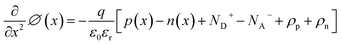 | (1) |
Here, ∅(x) and q are the electrostatic potential and elementary electron charge, εr and ε0 is the relative permittivity and permittivity of free space, p(x) and n(x) hole and electron concentrations (cm−3), ND+ and NA− is ionized donor and acceptor densities (cm−3), ρp and ρn is the hole and electron distribution.
Another important equation for the SCAPS-1D program is the continuity equation, which effectively calculates the rate of change of hole and electron carrier concentrations over position and time. The continuity equation describes how electrons or holes are generated, SRH recombined, or transported over time and space. It shortly expresses that the rate of change of carriers is equal to the net current flow + carrier generation – carrier recombination. The continuity equation can be described below with eqn (2) and (3):
Electron continuity equation
| |
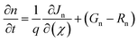 | (2) |
Hole continuity equation
| |
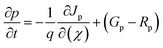 | (3) |
where,
Jn and
Jp stands for the current densities of electrons and holes.
Gn and
Gp depict the generation rate of electrons and holes. Lastly,
Rn and
Rp represent the recombination of holes and electrons.
Another important term for the simulation program is the carriers' drift-diffusion determination. Drift-diffusion characteristics are responsible for various factors, e.g., efficient charge collection, generation-recombination mechanism, interface, and ionic effects. Those properties are also a key indicator for the selection and choice of effective layers for any solar cell. The charge carrier drift–diffusion equation for electrons and holes can be expressed by eqn (4) and (5)
where,
µp,
µn,
Dn, and
Dp denotes the mobility of holes, mobility of electrons, diffusion coefficient of electrons, and diffusion coefficient of holes, respectively.
The performance parameters are the key factor to determine the overall effectiveness of any cell. For the evaluation of the parameters, the corresponding four parameters, including VOC, JSC, FF, and PCE has been maintained using the equations from (6)–(9)31,69,70
| |
 | (6) |
| |
 | (7) |
| |
 | (8) |
| |
 | (9) |
Here, the light-generated current and reverse saturation current are represented with
Jph, and
Jo. Also, Δ
n is the excess carrier concentration, and
k is the Boltzmann constant. Moreover,
Rs is a series resistance,
Rsh is a shunt resistance, and
V, and
J represent the applied voltage and current density.
For the absorption profile of the incident photon, the sqrt of Eg-model is chosen from the SCAPS-1D panel. This mathematical relation between the parameters for the absorption modeling can be expressed by the ‘Tauc law’ through eqn (10)–(12)
| |
 | (10) |
| |
 | (11) |
| |
 | (12) |
Here,
α,
Eg,
hv represents the coefficient of absorption profile, bandgap, and photon energy, sequentially. Additionally,
αo and
βo stands for the model parameters.
2.4. Machine learning algorithms
Machine learning (ML) can play a critical role in improving cell performance with high precision. For advanced cell manufacturing, ML has added a new dimension by using its predictive mechanism.71,72 Four supervised machine learning algorithms have been deployed to evaluate and predict the performance via a generated dataset of the SCAPS-1D package. The quick description of all four ML algorithms used in this study is given in the sections below:
2.4.1. Random forest. Random forest (RF) is a supervised non-parametric learning technique that combines both classification and regression techniques. It has built up in combination with the prediction of different trees that may reduce the overfitting. As an ensemble learning technique, RF constructs a magnitude of uncorrelated decision trees during the training phase by utilizing bootstrap aggregating and random feature selection to make the model more dynamic. This ML technique is superior for its robust functionality against noisy data for further enhancement of the prediction accuracy.73 The mathematical approach for this ML algorithm can be described as eqn (13).| |
 | (13) |
where, f(x) is the ultimate prediction and yi(x) is the ith prediction, and n is the number of trees.
2.4.2. Extreme gradient boosting. Extreme gradient boosting (XGBoost) is a powerful ensemble learning algorithm based on the gradient boosting framework, where multiple weak learners are sequentially combined to construct a strong predictive model. In XGBoost, decision trees are added iteratively, and each new tree is trained to minimize the residual errors produced by the previous ensemble. A distinctive feature of XGBoost is the regularization techniques to reduce the model complexity for significantly reduced data overfitting and enhance generalization performance. The algorithm incorporates both first and second order gradient information of the loss function while enabling faster convergence and highly accurate optimization in comparison with traditional gradient boosting methods. Due to its ability to capture non-linear relationships with input parameters, XGBoost is particularly suitable for modeling highly non-linear systems like PV devices.74 The model can be represented mathematically through eqn (14)| |
 | (14) |
where, fm(x), βi, and fi(x) is the cumulative prediction, assigned weight of the ith learner, and weak learning prediction of the ith learner, sequentially.
2.4.3. Categorical boosting. Categorical boosting (CatBoost) is a gradient boosting algorithm specifically developed to address the limitations of traditional methods to efficiently handle categorical and heterogeneous data. CatBoost employs an ordered boosting strategy that prevents target leakage and reduces prediction bias during the training procedure. This method ensures that the model learns from past observations, which makes this algorithm more stable and reliable. Furthermore, CatBoost automatically converts categorical variables using target-based statistical encoding with appropriate regularization. This phenomenon improves the learning efficiency without further preprocessing of the features. The training mechanism and reduced sensitivity to hyperparameter tuning make this model robust for regression-based performance prediction in solar cell optimization.75 The mathematical overview can be expressed as eqn (15).| |
 | (15) |
where, fo(x), γm, hm(x) is the initial predicted value, the learning rate for mth iteration, and mth weak learner trained on the residues of the previous step, respectively.
2.4.4. Decision tree. A decision tree (DT) is a non-parametric supervised learning algorithm that predicts outcomes by recursively partitioning the input features into smaller homogeneous regions. At each decision node, the algorithm picks the feature and corresponding threshold that effectively separates the data according to a predefined impurity criterion, which creates a tree-like hierarchical structure. This process continues until a stopping condition is met and predictions are obtained from the terminal leaf nodes. DTs are highly interpretable because of the underlying data structure and physical relationship between input and output responses. However, the overfitting tendency has arisen without constraints when the appropriate control of tree depth and minimum sample size is not carefully chosen.76 The mathematics behind this algorithm can be written as eqn (16)| |
 | (16) |
where, T, cm, and Rm is the total number of tree nodes, prediction values for mth, and mth disjoint region (leaf) of the feature space, accordingly.
3. Result and discussion
3.1. Thickness optimization of ETL and HTL
The thickness of CTLs is essential for improving the PCE of perovskite solar cells. To serve this purpose, a range of thickness boundaries is chosen to figure out the performance of the simulated structures. A systematic variation between 20 and 200 nm was examined to figure out the best thickness range for CTLs.77 The optimal thickness of ETL and HTL is crucial due to their elevated charge carrier mobility, diminished recombination losses, and effective charge extraction.78 The optimization of these layers enhances not only the efficiency of PSCs but also affects stability and charge transport dynamics.57 Consequently, meticulous regulation of energy bandgap alignment in CTL materials is imperative.
Fig. 3 portrays the variation impact of both ETL and HTL thicknesses to examine the ultimate PCE. According to the illustration of Fig. 3(a)-(c), ZnSe and WS2 ETLs exhibit a constant performance across the full thickness variation spectrum. This suggests that carrier extraction and recombination in these materials exhibit reduced sensitivity to the variations in ETL thickness. The configuraion of PC60BM exhibits lower thickenss sensitivity compared to the other configurations, as shown in Fig. 3(b). Conversely, SnS2 ETL has demonstrated a progressive decline in performance with increased thickness from Fig. 3(d). This is a major indication of elevated trap densities, diminished carrier mobilities, and augmented recombination losses.56 Among the ETL candidates, WS2 has exhibited the highest PCE of 19.21%, followed by ZnSe at 18.94%, PC60BM at 17.69%, and SnS2 at 16.80%, respectively. The outstanding performance of WS2 is proven for its bandgap of 1.8 eV and advantageous band alignment with PAL for enhanced and effective electron extraction. WS2 consists of tungsten atoms interspersed between hexagonally organized sulfur atoms, facilitating improved light absorption and charge transfer.31 In contrast, SnS2 and PC60BM have greater negative CBO values, which can result in an upshot of electrons at the ETL/absorber interface and diminished device performance. The best ETL thicknesses identified were 20 nm for WS2, ZnSe, PC60BM, and SnS2. For HTL CFTS, the PCE is rather stable across the same thickness variation range. This trend stands out as a major indicator of the negligible effect of HTL material thickness on hole transport and the generation, while improving charge collection by diminishing recombination.50 At an HTL thickness of 100 nm, similar peak efficiencies have been observed for ZnSe, WS2, PC60BM, and SnS2 ETLs.
 |
| | Fig. 3 CTLs thickness variation effect on PCE (a) ZnSe, (b) PC60BM, (c) WS2, and (d) SnS2. | |
3.2. Optimization of absorber thickness
Fig. 4 portrays the effect of absorber thickness variation in the simulation from 200 to 1500 nm. Firstly, the ETL and HTL thicknesses have been set to their optimized values, and then the optimal thickness of the absorber layer has been investigated in this section. The absorber layer (KGeCl3) is particularly crucial to mark the cruciality of effectively PSCs perform since it directly impacts the amount of light the photon absorbance, carriers' generation and recombination, electric field generation, and carrier spread out mechanisms.79 This layer's ability to effectively absorb incoming photons makes an electron hole pair (EHP). Moreover, the material internal parameters depend a lot on the perovskite material's natural properties, especially its bandgap.80 To produce an effective layer for absorbing light, it needs to stop recombination and make carriers last longer with a prolonged carrier lifetime. Making the absorber thicker improves both the built-in electric field and the diffusion length. These things work together to make it easier for the charge carrier to move.81
 |
| | Fig. 4 Alternation effect of absorber thickness on (a) VOC, (b) JSC, (c) FF, and (d) PCE, with four ETLs. | |
From the beginning, Fig. 4(a) shows a decline pattern in VOC due to the increased recombination rate for all four structures. As the absorber gets thicker, the short-circuit current density (JSC) rises quickly, as shown in Fig. 4(b). This is because the light is absorbed better, and the charge carriers are gathered more effectively. The larger JSC signifies that more electrons and holes are being created, so the carrier concentration is higher, and the current output is stronger.57 Both Fig. 4(a) and (c) show that with the thickness increasing, the VOC and FF are descending slowly. This pattern indicates increased recombination losses and falling charge extraction efficiency. Fig. 4(d) is the PCE curve with an observable peak at a 400 nm thick absorber, and thereafter slowly falling with WS2, ZnSe, and PC60BM after their optimum. While a thicker absorber increases photon absorption, it simultaneously increases the series resistance and the probability of carrier recombination before reaching the contacts.81 Thus, 400 nm represents the optimal balance between generation and collection efficiency. However, SnS2 configuration is best at a 300 nm layer thickness with its performance metrics. One important point to be noted, when the absorber is very thin, recombination is dominant because there are few carriers around to absorb incoming light. If we make it too thick, less charge can be produced from light because there's not enough surface area for photons to interact with our material.53 Therefore, the correct thickness allows most light to create charge whilst losing the least to defects. Finally, Fig. 4(d) demonstrates that at their respective best absorber thicknesses, different ETL materials can achieve the highest efficiencies of 19.46% for WS2, 19.24% for ZnSe, 17.83% for PC60BM, and 17.40% for SnS2. This study finds that 400 nm is the best thickness of KGeCl3 absorber for WS2, ZnSe, and PC60BM, but 300 nm is the optimum one for SnS2 structure.
3.3. Optimization of ETL donor density
In PSCs, donor density (ND) is an important term to determine free electron conductivity, charge separation efficiency, recombination losses, optical characteristics, and finally the overall performance of the device.67 A boost in donor density means the appearance of additional free electrons, which will change the electronic configuration and performance characteristics of PSCs. In this study, we try to investigate the optimal donor densities of different electron transport layers (ETLs). The initial defect densities of the ETLs are shown in Table 1, where 1018 cm−3 for WS2 and ZnSe, 1017 cm−3 for PC60BM, and SnS2. Fig. 5 plots the change in donor densities from the range of 1012 cm−3 to 1022 cm−3. As can be seen from Fig. 5(a), the VOC of ZnSe, WS2, and SnS2 remains almost constant for a long time to 1016 cm−3. Beyond this, it begins to increase till the rest of the portion. In contrast, PC60BM maintains an unvarying VOC up to 1018 cm−3, then suddenly drops off at 1020 cm−3 before climbing back up by 1022 cm−3. The increase in VOC indicates a proper band alignment and less recombination at high donor densities. Then, in Fig. 5(b), the JSC for all ETLs remains nearly the same within the variation range. This is an indicator that carrier generation and absorption of light by the ETL are not largely affected by variation in ND. Likewise, as shown in Fig. 5(c), the FF has a similar trend to VOC, with all ETLs showing a considerable improvement at higher donor concentrations. A high FF, which denotes good conductivity and rapid electron transport within the ETL, clearly impacts the PCE of all structures which as visualized in Fig. 5(d). For ZnSe, SnS2, and WS2, the PCE stays constant up to 1016 cm−3, then begins to rise after that. As for PC60BM, PCE remains level until 1018 cm−3, from which point it makes a sudden leap up at 1022 cm−3. The optimization of the ND produced dynamic results; it achieved a maximum PCE of 19.49% with WS2, 19.47% with ZnSe, 18.91% with SnS2, and 17.83% with PC60BM configuration. The accompanied increase of VOC and FF, together with almost unchanging JSC, combine to produce significant gains in device efficiency. Through optimization, charge extraction is improved, series resistance is reduced, and band alignment becomes sharper. These enhancements are thought to be the reason for increased capacitance and lengthened carrier lifetime. Furthermore, the optimal ETL donor densities were determined to be 1020 cm−3 for WS2, ZnSe, and SnS2, as well as 1017 cm−3 for PC60BM. Among the structures examined, the FTO/WS2/KGeCl3/CFTS structure overall gave the best performance.
 |
| | Fig. 5 Performance parameters with the variation of ND of ETL (a) VOC, (b) JSC, (c) FF, and (d) PCE. | |
3.4. Optimization of HTL acceptor density
The acceptor density (NA) of the HTL is very important for controlling carrier transport, interfacial recombination, and the overall PCE. CFTS is a comparatively stable and low-cost material with better optical and electrical performance.82 When the HTL acceptor density goes from 1013 to 1017 cm−3, the PV parameters don't change much, as shown in Fig. 6. The VOC exhibits low, the FF shows moderate, and the PCE is relatively poor in the variation region up to 1018 cm−3. In this low-doping regime, the weak band bending at the HTL/absorber interface does not create enough built-in potential for efficient charge separation. This makes it take longer to extract holes and increases recombination losses. The built-in electric field at the interface gets stronger when the doping density goes beyond 1019 cm−3. This speeds up carrier transport and slows down recombination at the heterojunction, which improves both VOC and FF. In the high doping range of 1021 to 1022 cm−3, there is a gradual and sharp improvement in the performance parameters. The HTL makes a very conductive path for hole transport, lowers series resistance, and makes it easy to make almost ohmic contact at the interface. The PCE goes up a long way till 1020 cm−3, with the highest efficiencies being 21.47% for WS2, 21.46% for ZnSe, and 20.75% for SnS2, as well as 19.94% for PC60BM configurations. The JSC stays almost the same across the whole doping range. This shows that HTL doping mostly affects electrical processes and not optical ones, and does not affect the creation of photocarriers. With previous studies, the JSC curve stays virtually the same when the NA of the absorber layer changes from 1014 to 1018 cm−3. However, when the doping level gets close to 1022 cm−3, the curve drops sharply because Auger and trap-assisted recombination start to happen.83 These recombination processes shorten the lifespan of carriers that eventually make the depletion region smaller and limit the diffusion length.84 This makes it harder for carriers to aggregate and lowers the photocurrent. This trend shows the importance of finding the right balance between doping concentration. A high HTL acceptor density is good for device performance, but too much absorber doping leads to a lowering of overall efficiency.
 |
| | Fig. 6 Acceptor density variation impact of HTL on performance parameters. | |
3.5. Impact of acceptor density variation of absorber
Initially, the absorber acceptor density was set to 1015 cm−3. The acceptor density (NA) varies from 1012 to 1022 cm−3. In Fig. 7(a), the VOC remains constant at 1014 to 1016 cm−3; after that, it noticeably increases up to 1022 cm−3. The rising VOC implies a strong build-up in the electric field, which improves the separation of carriers. Fig. 7(b) illustrates the JSC curve, at 1012 to 1017 cm−3, the JSC curve remains almost constant, then remarkably goes down at 1022 cm−3. The parameter JSC has a reverse impact on the absorber layer, decreasing the short-circuit current with respect to higher NA, resulting in high Auger or trap-assisted recombination, a narrow depletion region, and reduced diffusion length.58,68 Again, Fig. 7(c) describes that the FF fluctuates up to 1017 cm−3, then significantly rises to the maximum point at 1020 cm−3. The rising trend of FF improved charge transport and lower series resistance. Lastly, the PCE trend for all configurations is described in Fig. 7(d). On a careful look, the VOC and FF are increased; as a result, the overall performance is also improved. Furthermore, it is observable from the study that the increase beyond a threshold, absorber NA, depicts a bulk amount of recombination loss, high diffusion, and trap density state. However, an adequate amount of NA appropriately affects device generation and recombination. Therefore, we have selected the optimized value of NA at 1017 cm−3 for all ETL materials with the best performances for WS2, ZnSe, PC60BM, and SnS2 ETLs of 21.59%, 21.58%, 21.46% and 20.45%, respectively.
 |
| | Fig. 7 Variation impact of absorber NA on cell performance (a) VOC, (b) JSC, (c) FF, and (d) PCE. | |
3.6. Defect density variation impact of ETL and HTL
Fig. 8 expresses the performance variation of CTLs with respect to their individual defect density. Nt is a supreme determinant due to the direct influence on charge separation and generation of PSC.26,85 Additionally, Nt has a direct influence on the generation, recombination, and carrier lifetime.65 Initially, the Nt of the ETL materials WS2, ZnSe, and PC60BM was considered to be 1015 cm−3, and SnS2 was assigned a Nt of 1014 cm−3. Similarly, the Nt of the HTL was set at 1015 cm−3. As shown in Fig. 8, the variations in ETL defect density and HTL defect density indicate that the photovoltaic parameters VOC, JSC, FF, and PCE remain nearly constant up to 1016 cm−3. Beyond this threshold, however, JSC and PCE begin to decline, particularly in the case of WS2 and PC60BM materials. Moreover, it shows that variations in the HTL Nt display negligible influence on device performance, as the values of performance parameters remain almost unchanged across all four device structures. After optimizing Nt of ETL and HTL, the simulated PCEs for the four different structures were found to be 21.59%, 21.58%, 21.46%, and 20.45% for WS2, ZnSe, PC60BM, and SnS2, accordingly. These findings indicate that the ETL and HTL defect densities have a lower impact on the overall device performance. Therefore, we have marked the optimized ETL and HTL defect density as an initial value.
 |
| | Fig. 8 ETL and HTL's defect density variation impact on performance (a) ZnSe, (b) PC60BM, (c) WS2, and (d) SnS2. | |
3.7. Effect of variation in absorber defect density
The number of absorber defects is important for the impact on charge carriers' movement, recombination, and energy levels. This is a more dominating effect on performance than ETL and HTL.78 In Fig. 9, the device parameters show clear changes as the defect density goes up. When the defect density is modest in the range between 1012 to 1014 cm−3, VOC, FF, and PCE only go down a little, and JSC stays almost the same. This stability in JSC indicates that the photogeneration rate and carrier extraction are not substantially impacted at low trap densities via facilitating effective carrier collection. However, the defect density goes above 1014 cm−3, deep and shallow traps in the absorber start to take over. These traps operate as a recombination accelerator that speeds up non-radiative SRH recombination.86 The ongoing drop in VOC is caused by more recombination losses for lowering the quasi-Fermi level splitting between electrons and holes as Nt goes up.57 This is an important factor in determining VOC. The drop in FF is also due to trap-assisted recombination and higher series resistance.50 JSC stays the same up to about 1017 cm−3, which means that photogeneration isn't significantly affected. But when defect concentrations are higher than this, recombination happens faster than carrier transport and drop photocurrent sharply. This change shows the internal electric field is weaker because of less drift-assisted carrier collection and boosts bulk recombination.77 The simultaneous decrease in PCE is the result of a combination of lower VOC, worse FF, and lower JSC. So, it's important to manage the Nt of the absorber in order to make the device work better. This work shows that the best and optimal defect density is 1014 cm−3, where recombination losses are low, and carrier transport is still efficient. In this case, the greatest PCE values for all ETLs are listed for WS2 for 22.33%, ZnSe for 22.32%, PC60BM for 21.95%, and SnS2 for 21.13%, respectively. This shows that reducing trap states in the absorber not only makes photovoltaic parameters more stable, but it also makes perovskite solar cells last longer and work better over time.
 |
| | Fig. 9 Variation effect of absorber defect density on cell performance. | |
3.8. Optimization of interface defect density
The defect density of the interface layer between the absorber/ETL layer (IL1) and the HTL/absorber layer (IL2) impacts the perovskite device performance, especially on the external quantum efficiency (QE).87 Hence, the necessity of optimization plays an inevitable role in enhancing the light absorption spectra while maintaining better stability and performance. In this study, Fig. 10 depicts the absorber/CTL total interface defect density with variations from 1010 to 1018 cm−2 for (a) ZnSe, (b) PC60BM, (c) WS2, and (d) SnS2 structures. The performance shown in these contour plots remains predominantly similar in nature across WS2, ZnSe, and SnS2 materials. The low-defect zone (below 1013 cm−2) has the highest efficiency, whereas deterioration is significant above 1014 cm−2. Better electronic coupling and lower non-radiative recombination losses are indicated by ZnSe and WS2, which also show improved interface tolerance and sustain PCE values above 20% throughout a larger defect range. On the other hand, even at relatively low defect densities, PC60BM exhibits a sharp decline in PCE, which indicates inadequate interface stability with the KGeCl3 absorber. In comparison to ZnSe and WS2, SnS2 exhibits moderate stability and a marginally lower peak efficiency. ZnSe and WS2 are the most attractive ETL choices for high-performance lead-free KGeCl3 perovskite solar cells. Overall, the results show that limiting interface defect concentrations, especially below 1013 cm−2, is crucial for obtaining optimal device efficiency. Therefore, we selected the optimized interface defect density of HTL/KGeCl3 and ETL/KGeCl3 at 1010 cm−2, based on the maximum performance. The best performance of the four different ETLs WS2, ZnSe, PC60BM, and SnS2 is 22.33%, 22.32%, 21.95%, and 21.13%, respectively.
 |
| | Fig. 10 Variation impact on PCE of (a) ZnSe, (b) PC60BM, (c) WS2, and (d) SnS2 with interface defect density. | |
3.9. Effect of back contact on performance
A good back contact is essential for a high-performing and stable PSC. It directly determines the charge extraction efficiency and the device's total lifespan.88 The back electrode serves not only as a physical layer but also plays a crucial role in determining the efficiency of carrier movement across the interface. Poor band alignment results in increased resistive losses, recombination, and diminished overall performance.89 In our study, we have tuned the back contact work function between 4.2 and 5.2 eV to see how it affects the PCE of PSCs with different ETLs (ZnSe, PC60BM, WS2, and SnS2). The visual representation of work function change in back contact can be found through Fig. 11. Primarily, due to poor band alignment and ineffective charge carrier extraction, the PCE slightly changes at the lower end (around 4.2–4.6 eV). However, there is a consistent improvement after the work function surpasses 4.6 eV, and the effect peaks between 4.8 and 5.2 eV. This is the area where the interface promotes freer charge movement, inhibits recombination, and reduces energy loss. At roughly 5.1 eV, which coincidentally corresponds to the work function of gold (Au), the highest performance is observed.57 This makes sense because Au forms an almost perfect energy level alignment with the primary absorber in addition to offering superb conductivity. At the same time, it minimizes losses while enabling effective hole collection towards the electrode. For this reason, Au is the ideal material for our study's final device structure, with the best performance coming from the constructed FTO/WS2/KGeCl3/CFTS/Au structure, with the recorded amount of PCE of 22.43%. This is one of the configurations that leads to long-term stability, easy carrier extraction, and maximum efficiency with this configuration.
 |
| | Fig. 11 Work function alternation impact on PCE of different structures. | |
3.10. Effect of parasitic resistance on cell performance
The performance of a PSC is strongly influenced by two key electrical factors, namely series resistance (Rs) and shunt resistance (Rsh).3 This parasitic resistance has a direct influence on the performance parameters. Conceptually, low Rs and high Rsh create the best conditions for stable and efficient operation. As Rs increases, the efficiency rapidly drops, regardless of Rsh.3 This happens because higher series resistance limits current flow, introduces resistive losses, and distorts the current–voltage curve.90 On the other hand, Rsh decreases below 103 Ω cm2 introduces leakage currents and improved recombination on the cell.3
Fig. 12 represents the variation effect of both parasitic resistances, i.e., Rs and Rsh. Among the four distinct ETLs, WS2 and ZnSe stand out for maintaining the highest PCE values even under moderately high Rsh. This highlights their strong compatibility with the absorber. Another ETL PC60BM performs slightly lower but still shows a stable profile. Lastly, SnS2 gives the weakest performance among all the ETLs. This analysis reinforces that controlling both resistances is extremely important, besides optimizing the absorber and contacts. The optimal operating condition has been determined for low series resistance (<1 Ω cm2) with high shunt resistance (>104–106 Ω cm2) for extracting maximum power from the simulated devices. From this study, the best balance and optimization is achieved at Rs and Rsh of 1 Ω cm2 and 106 Ω cm2, respectively. Under these optimized conditions, the highest efficiencies have been recorded as 21.39% for WS2, 21.38% for ZnSe, 21.05% for PC60BM, and 20.43% for SnS2, accordingly. These results clearly show the smooth charge transport, minimal losses, and reliable long-term performance of the device.53,65
 |
| | Fig. 12 Contour plot of series resistance and shunt resistance variation on the PCE (a) ZnSe, (b) PC60BM, (c) WS2, and (d) SnS2. | |
3.11. Effect of operating temperature
The temperature also has a significant impact on PV performance and device stability. The increasing trend in device temperature leads to high recombination, which reduces the VOC and causes material and interface degradation.60,69,91 For better understanding, the VOC, JSC, and Jo's relation with the temperature equations given in (17)| |
 | (17) |
In Fig. 13, the temperature variation is taken from 300 to 420 K for comparison with the real environment. The VOC, FF, and PCE gradually decrease with rising temperature because of thermal instability, increasing series resistance, worsened charge collection, and increased leakage paths.69 When the temperature (T) increases, the thermal energy increases, and the dark saturation current (Jo) increases exponentially due to enhanced intrinsic carrier concentration and recombination, resulting in VOC gradually decreasing.65 Moreover, the FF and VOC are proportional to the PCE due to decreased efficiency. But the JSC remains constant because of the better carrier mobility, the photogeneration rate remains unchanged, and high light absorption. At a room temperature of 300 K, the best PCEs are obtained for four different ETL configurations of WS2, ZnSe, PC60BM, and SnS2, which are 21.39%, 21.38%, 21.05% and 20.43%, respectively.
 |
| | Fig. 13 Effect of temperature on four different structures on cell parameters. | |
3.12. Optimized J–V and QE curve
In this study, we optimized four different ETL configurations with WS2, ZnSe, PC60BM, and SnS2-based structures using a KGeCl3 absorber material and CFTS as hole transport material. The thickness of the ETLs and HTL has been varied in a range of 20 nm to 200 nm, while the thickness of the absorber material has been adjusted between 200 nm and 1500 nm. Additionally, the ND of the ETL varies from 1012 to 1022 cm−3, and the NA of both the absorber and HTL has also been analyzed over a range of 1012 to 1022 cm−3. The Nt of the absorber, HTL, and ETL materials was varied from 1012 to 1018 cm−3. Moreover, the interface defect densities at both the ETL/absorber and HTL/absorber junctions were adjusted from 1010 to 1018 cm−2. After final optimization, the PCE for the four distinct ETLs has been found to be as follows: 21.39% for WS2, 21.38% for ZnSe, 21.05% for PC60BM, and 20.43% for SnS2 accordingly. These results indicate that optimization significantly improved the PCE of all materials. On a careful look, it is proven that WS2 achieves the highest efficiency, closely followed by ZnSe. The enhancements in PCE result from optimized material characteristics, including decreased defect density, enhanced crystalline properties, and improved charge transport.
Fig. 14(a) and (b) presents the J–V characteristics for the four ETL configurations. The trend of the illustration reveals the JSC increment at lower values of VOC. This behavior emphasizes the balance between the generated VOC and JSC to achieve the maximum PCE in PV devices. The initial J–V structures illustrate the results derived from the simulation described in Fig. 14(a). It also shows the J–V characteristics of the ETL with the highest performance, WS2, which shows that it is still the best-performing ETL even in its initial state. The optimized J–V curves from Fig. 14(b) again show the highest PCE by WS2, which confirms its superior performance as an ETL material in this study. The curve shows that the device has a higher VOC and JSC, which gives it the highest PCE of all the materials examined. This graph highlights that WS2 was successfully optimized, which led to a big increase in the efficiency of the device. Fig. 14(c) displays the improved devices' QE as a function of wavelength for the initial condition. The graph shows that the conversion of photons to electrons is quite good in the visible range, which is the section of the solar spectrum with the maximum energy. The device gets almost 100% QE from 400 nm to 700 nm of the incident photons. This means that the material is very good at turning photons into electrical charge in the visible range. This is significant for making solar cells work efficiently because the visible light spectrum makes up a large part of the total solar energy available. Fig. 14(d) shows the optimized QE for the best-performing technology. Here again, WS2 shows even more potential in the photon conversion to electrons. The graph simultaneously confirms that WS2 has a high QE over the visible spectrum and the ability to collect and transform light energy more efficiently. WS2 is remarked as the best ETL material in this investigation because it has a near-perfect QE spanning the 400 to 700 nm range. The KGeCl3 absorber, CFTS HTL, and the ETLs altogether have contributed a significant number to the elevated device outcome. These results remind the importance of optimizing material parameters like defect densities, thicknesses, and donor/acceptor concentrations to make an upgraded optoelectronic device for the next PV era.
 |
| | Fig. 14 (a) Initial, and (b) optimized J–V curve, (c) initial, and (d) optimized QE for all four different structures. | |
3.13. Analysis of the generation and recombination rate
Generation and recombination mechanisms are one of the core phenomena of solar cells. This is an utmost indicator to understand the generated carrier density ready to collect. In Fig. 15(a) and (b), the initial and optimized generation rate values for all four structures are illustrated. The optimized generation of all materials shows a smoother curve and increased overall performance. Also, it is suggested that a high magnitude, smoother distribution, and reduced recombination at the interface for the carrier. The overall generation rate across 0.1 to 0.6 µm shows its peak for all four structures. For mathematical calculation, the generation profile of carriers can be calculated by eqn (18),69| | |
G(λ,x) = α(λ,x) × Nphot(λ,x)
| (18) |
where, G(λ,x), α(λ,x), and Nphot(λ,x) stands for generation profile, absorption profile, and incident photon flux, sequentially.
 |
| | Fig. 15 (a) Initial, (b) optimized generation rate, (c) initial, and (d) optimized total recombination rate. | |
Fig. 15 also illustrates the overall position-dependent generation and recombination profiles of four distinct ETL configurations with multilayer solar cells under AM 1.5G light, contrasting the initial and optimized configurations. In the initial device structure from Fig. 15(a), the carrier production profile progressively increases across the absorber but displays significant spatial non-uniformity at the same time. This non-uniformity signifies an uneven optical field distribution and non-uniform photon absorption, resulting in enhanced interfacial recombination and inefficient carrier extraction. Conversely, the improved device from Fig. 15(b) exhibits a far smoother and robust generation profile with peak values nearing 2 × 1022 cm−3 s−1 with the optimized WS2-based structure. This enhancement results from structural modification, such as adjusting the thickness value of active layers, matching intermediate band alignment, or a higher optical absorption coefficient of layer materials.86 Those properties facilitate improved light trapping and capture of the incident photon spectrum from the sun. The recombination profiles with Fig. 15(c) further reinforce the impact of optimization. The initial structure has a recorded recombination peak of approximately 1.7 × 1020 cm−3 s−1 near the absorber/ETL interface. This finding indicates substantial interfacial defect-assisted recombination. This peak also signifies that charge carriers generated near the interface are rapidly dissipated before they can contribute to the photocurrent.83 In the post-optimization scenario of WS2 configuration, the recombination peak is markedly reduced to around 7.91 × 1019 cm−3 s−1, which is visible from Fig. 15(d). The occurrence of recombination indicates improved electronic quality of the junctions, perhaps due to better band alignment between the absorber and buffer layers, reduced defect density by interface passivation, or appropriate doping concentrations after optimization.50,92 The concurrent rise in carrier generation and decline in recombination indicates a comprehensive enhancement in the optical management and electrical quality of the device.93 These enhancements are expected to increase carrier collection efficiency, reduce losses, and thus improve PV performance metrics.94
3.14. Earlier studies comparison
Perovskite is a trendy research topic in this decade for its potential to create a breakthrough for the next generation of PV technology. To push up the ongoing enhancement, optimization is a must to meet requirements because of its necessity for making an efficient solar cell by eradicating all boundaries and constraints. Additionally, the process helps to make a cost-effective, durable, and reliable PSC in real life. In our study, we have conducted a full set optimization of absorber layer, ETL, and HTL parameters for maximizing the performance metrics. The optimization process has made a remarkable change in initial efficiency and ensures the stability of the simulated structures.
The study represents the outcome of KGeCl3-based PSC through SCAPS-1D simulation. Alike types of numerical studies had been conducted previously. But one of the major concerns of this study is the lack of experimental validation with the same materials in contemporary times. It is extremely rare to see the particular KGeCl3 perovskite absorber used for practical synthesis or manufacturing, to the author's best knowledge. But, Ge-based perovskite is a wide and potential weapon to replace the traditional lead-based perovskite, which is extremely hazardous both for human health and the environment.28 A few years back, in 2018, a comparatively nearby Ge-based structure of ITO/PEDOT:PSS/MAGeI2.7Br0.3/PC70BM/Ag reported a poor PCE of 0.57% due to the practical synthesis boundary for higher parasitic resistance.95 Other lead-free alternatives have been actively explored to address these concerns. Commonly, Sn-based absorbers such as CsSnI3 integrated into ITO/PCBM/CFTS/Se structures have delivered PCEs of 24.73% with JSC values approaching 34 mA cm−2.67 Similarly, double perovskite systems such as Cs2PtI6 in an FTO/SnS2/Cs2PtI6/MoTe2/Au configuration reported PCE as high as 32.98%,85 though challenges in large-scale fabrication and stability persist. Germanium-based one can be a potential solution reported in prior studies. Against this background, KGeCl3 has recently emerged as a promising germanium-based perovskite alternative. Prior studies on KGeCl3 absorbers demonstrated efficiencies ranging from 15% to 29%, depending on device architecture.25–27,29 These results confirm that KGeCl3 can deliver competitive efficiencies comparable to or exceeding many lead-free systems.
The optimized device structure of FTO/CFTS/KGeCl3/WS2/Au has achieved the highest PCE of 21.39%, with a VOC of 0.706 V, JSC of 39.526 mA cm−2, and FF of 76.56% in this work. Other comparable efficiencies have been observed for ZnSe (21.38%), PC60BM (21.05%), and SnS2 (20.43%) as ETLs at the same time. A complete list of prior studies and our conducted study is highlighted in Table 4. Although these values are slightly lower than the highest reported KGeCl3 devices in literature, they remain significantly higher than several earlier experimental reports, for example, 15.83% for FTO/SnS2/KGeCl3/Cu2O/C.26 The strong JSC values observed in this study (39–40 mA cm−2) indicate enhanced light absorption and efficient carrier collection due to careful selection and optimization of transport layers. KGeCl3 has competitive performance with the added benefit of non-toxicity and probable long-term stability, making it an appealing contender for sustainable solar applications, even if lead-based perovskites continue to have the greatest reported efficiencies. All things considered, the comparison shows that KGeCl3 is a feasible lead-free perovskite absorber that can achieve efficiencies higher than 21% in ideal simulated conditions.
Table 4 Comparative assessment of PV parameters for different KGeCl3-based and other reported solar cells
| Typea |
Device structure |
VOC (V) |
JSC (mA cm−2) |
FF (%) |
PCE (%) |
Year |
Ref. |
| E = experimental, T = theoretical. |
| E |
FTO/SnS2/Cs0.05(FA0.83MA0.17)0.95Pb(I0.83Br0.17)3/Spiro-OMeTAD/Au |
0.99 |
20.75 |
67.00 |
13.77 |
2020 |
36 |
| E |
ITO/PCBM/MAPbI3/PEDOT:PSS/Ag |
0.971 |
19.04 |
46.54 |
8.60 |
2023 |
96 |
| T |
FTO/TiO2/KGeCl3/Spiro-OMeTAD/Au |
1.02 |
25.77 |
78.25 |
22.98 |
2025 |
25 |
| T |
FTO/SnS2/Sr3PBr3/Sr3NCl3/Ni |
1.27 |
26.44 |
90.14 |
30.32 |
2024 |
77 |
| T |
ITO/PCBM/CsSnI3/CFTS/Se |
0.87 |
33.99 |
83.46 |
24.73 |
2023 |
67 |
| T |
FTO/SnS2/Cs2PtI6/MoTe2/Au |
1.11 |
33.19 |
88.89 |
32.98 |
2024 |
85 |
| T |
ITO/WS2/KGeCl3/CBTS/Ni |
0.679 |
41.439 |
78.12 |
22.01 |
2024 |
97 |
| T |
FTO/WS2/KGeCl3/PEDOT:PSS/Au |
1.19 |
30.08 |
82.74 |
29.82 |
2024 |
98 |
| T |
FTO/SnS2/RbPbI3/MoO3/Ni |
1.22 |
32.21 |
83.27 |
32.72 |
2025 |
99 |
| T |
FTO/WS2/KGeCl3/MoO3/Au |
0.88 |
41.45 |
81.76 |
29.83 |
2024 |
31 |
| T |
FTO/SnS2/KGeCl3/Cu2O/C |
0.545 |
41.91 |
69.24 |
15.83 |
2024 |
26 |
| T |
FTO/CSTO/KGeCl3/nPB/Au |
0.815 |
41.804 |
85.97 |
29.30 |
2025 |
29 |
| T |
FTO/ZnSe/NaZn0.07Ag0.3Br3/ZnTe/Au |
1.59 |
21.90 |
78.92 |
27.59 |
2024 |
94 |
| T |
FTO/SnS2/AgCdF3/C6TBTAPH2/Au |
0.86 |
41.23 |
86.68 |
30.81 |
2026 |
100 |
| T |
FTO/WS2/KGeCl3/CFTS/Au |
0.706 |
39.526 |
76.56 |
21.39 |
2025 |
This work |
| T |
FTO/ZnSe/KGeCl3/CFTS/Au |
0.706 |
39.525 |
76.55 |
21.38 |
2025 |
This work |
| T |
FTO/PC60BM/KGeCl3/CFTS/Au |
0.706 |
39.215 |
75.98 |
21.05 |
2025 |
This work |
| T |
FTO/SnS2/KGeCl3/CFTS/Au |
0.704 |
37.791 |
76.72 |
20.43 |
2025 |
This work |
The considerable variation in PV performance parameters has reported in Table 4 from fundamental differences in device architecture, material selection, and research methodology. The distinction between theoretical simulations and experimental studies is particularly significant. Previously reported simulations often predict higher efficiencies by assuming several factors, like ideal interfaces, optimal band alignment, and minimal defect densities. Conversely, experimental results must face the real-world challenges such as film non-uniformity, interfacial recombination, and material degradation.4,10 For example, the theoretical PCEs exceeding 29% for KGeCl3-based cells utilize CTLs like Spiro-OMeTAD, PEDOT:PSS, or MoO3.31,98,101 These types of materials provide excellent band alignment. But they are known to compromise long-term stability due to hygroscopic and thermal instability.80,99,102 In contrast, our study intentionally employs a fully inorganic stack like WS2 as the ETL and CFTS as the HTL. The choosing criterion prioritizes environmental resilience and thermal stability over absolute peak efficiency. The architectural choice for this study results in a slightly lower simulated PCE compared to some theoretical benchmarks, but the whole optimization has done with keep in mind to manufacturable pathway for practical device manufacturing. For our study, the WS2-based structure shows a shallow spike alignment (ΔEc = +0.05 eV), which facilitates efficient electron extraction while suppressing interface recombination. On the other hand, SnS2's cliff-type alignment can enhance interfacial losses if not properly passivated. Thus, our optimized efficiency of 21.39% with WS2 should be interpreted as a balanced achievement. Moreover, this architectural design focuses on respectable performance with enhanced durability and environmental compatibility for the next-generation PSC.
4. Machine learning integrated exploration
The machine learning (ML) analysis highlights a critical insight into the complex physics governing PSC performance. This previous observation strongly justifies the use of an advanced ensemble machine-learning model to capture higher-order interactions beyond the scope of conventional model simulation.71,74,90 This combined predictive–interpretive analysis demonstrates as a powerful surrogate for physics-based device analysis.
4.1. Correlation matrix analysis
The CTLs and absorber material's intrinsic parameters in from of a correlation matrix measured through the SCAPS-1D study and as anticipated by machine learning are shown in Fig. 16. This quantifies the linear correlations among the important device characteristics, where positive numbers imply direct linear relationships, whereas negative values indicate inverse linear dependencies. There is low multicollinearity in the dataset, as seen by the weak pairwise linear correlations among most input features in the correlation map. It is confirmed that the dataset covers a large and physically relevant parameter space free of artificial coupling by the near-zero off-diagonal values of thickness, doping densities, and defect densities. The absorber layer thickness has the strongest association with PCE (r = −0.294) out of all the input parameters, indicating a substantial inverse linear relationship. While a thicker absorber improves optical absorption, an overly thick one might make bulk recombination and carrier transport constraints worse, leading to decreased efficiency. This behavior is a result of a basic trend in semiconductor device physics. The relation with ML models has an edge over linear regression methods because they can capture this nontrivial equilibrium. It is consistent with the known role of trap-assisted Shockley–Read–Hall recombination in limiting carrier lifetime and quasi-Fermi level splitting. The effect of absorber Nt exhibits a clear negative correlation with PCE (r = −0.147). On the other hand, there is a considerable dependence on charge-selective contacts and interfacial energetics for the nonlinear impact of transport layer defect concentrations on device performance. They have shown almost nonlinear association with PCE.
 |
| | Fig. 16 Pearson correlation matrix representation between different features. | |
Notably, the trained ML model confirms its extraordinary prediction accuracy and consistency by showing an almost perfect linear correlation (r = 0.995) between the expected and real PCE from SCAPS-1D. The fact that the model has learned physically relevant associations instead of false statistical artifacts is further supported by the near-identical correlation patterns of PCE and predicted PCE with respect to all input features.
4.2. Analysis of prediction vs. actual values for different algorithms
Fig. 17 represents all four-machine learning (ML) algorithms that can reveal the relation between the actual and predicted PCE for all four structures. It presents the parity plots comparing calculated (actual) and machine-learning-predicted power conversion efficiency (PCE) values using four different regression models: (a) RF, (b) XGBoost, (c) CatBoost, and (d) DT. The reason behind choosing this model for their consistent performance for this kind of similar analysis from past.71–74 The RF model for Fig. 17(a) demonstrates a strong linear correlation between predicted and actual PCE values, while most data points are closely clustered around the ideal line. This incident indicates the event of high predictive reliability and minimal systematic bias. Again, a comparable trend is observed for the XGBoost model via slightly tighter clustering in the mid-to-high PCE range from Fig. 17(b). This algorithm potentially reflects the capability to capture nonlinear feature interactions to enhance the PSC performance.
 |
| | Fig. 17 Comparison of actual vs. predicted PCE with four supervised ML algorithms (a) RF, (b) XGBoost, (c) CatBoost, and (d) DT. | |
Among all models, CatBoost exhibits the closest agreement with the ideal prediction line across the entire PCE range from Fig. 17(c). The algorithm CatBoost always suggests superior generalization and robustness against overfitting.103 In contrast, the DT model in Fig. 17(d) displays a relatively larger dispersion of data points at higher PCE values. This trend implies reduced predictive stability due to its inherent sensitivity to data partitioning. Overall, the parity analysis shows that ensemble learning techniques, particularly CatBoost and XGBoost, greatly outperform for this study. Those algorithms are demonstrating their efficacy for precise and trustworthy PCE prediction in PSC optimization.
4.3. SHAP interpretability analysis
Fig. 18 illustrates the SHapley Additive exPlanations (SHAP) summary plots for (a) RF, (b) XGBoost, (c) CatBoost, and (d) DT models. All four models provide a transparent and quantitative interpretation of individual device parameters to influence the predicted PCE. Each point represents a sample and is colored according to the feature magnitude (low to high), while the horizontal axis indicates the SHAP value corresponding to the feature's impact on model output. The mean SHAP value for the corresponding features is also represented adjacent to it.
 |
| | Fig. 18 SHAP-based interpretation of feature contributions to PCE (a) RF, (b) XGBoost, (c) CatBoost, and (d) DT. | |
Across all models, NA of HTL (Acceptor_Density_HTL) emerges as the most influential parameter for consistently exhibiting the largest SHAP value spread. Higher acceptor densities predominantly contribute positively to PCE enhancement.3 Not only that, the magnitude of NA is certainly manipulating their critical role in improving hole extraction and reducing interfacial recombination losses. Moreover, a higher NA of HTL creates a stronger electric field by enhancing hole extraction efficiency through suppressing electron back-flow into the absorber. Thereby, this phenomenon dramatically reduces interfacial recombination. This dual role makes it the most sensitive parameter for VOC and PCE, as confirmed by device physics.104 Following this similar pathway, the absorber layer thickness ranks as the second most significant factor, where optimal thickness values positively affect PCE while excessively high values show a diminishing or negative contribution due to increased bulk recombination. The ND of the ETL also shows a notable positive influence for ensemble models. This indicates the importance doping profile in facilitating efficient electron transport. Conversely, defect densities within the absorber and transport layers generally exhibit negative SHAP values at higher magnitudes. This is an indicator for confirming that increased trap states adversely affect device performance by promoting non-radiative recombination.
In an important note, CatBoost and XGBoost display smoother and more consistent SHAP distributions compared to the DT model by reflecting their superior interpretability. These findings not only validate the physical relevance of the learned features but also demonstrate that SHAP-assisted machine-learning analysis can reliably bridge data-driven predictions with device physics through offering actionable guidelines for practical solar cell design.
4.4. Machine learning performance evaluation
Table 5 mentions the predictive performance of all four supervised learning models, including RF, XGBoost, CatBoost, and DT, while evaluating the model performance with the assistance of Root Mean Squared Error (RMSE), Mean Absolute Error (MAE), R2-coefficient (R2), Mean Absolute Percentage Error (MAPE), and accuracy. All these metrics highlight their corresponding model potential for improving the physical structure of the simulated solar cells. The mathematics for the performance evaluator can be written as eqn (19)–(23)| |
 | (19) |
| |
 | (20) |
| |
 | (21) |
| |
 | (22) |
| |
 | (23) |
where, yi, ![[y with combining caron]](https://www.rsc.org/images/entities/i_char_0079_030c.gif) i, ȳi, n, TP, TN, FP, and FN stand for actual/observed value, predicted/forecasted value, mean of actual values, total observation/data point, true positive, true negative, false positive, false negative, respectively.
i, ȳi, n, TP, TN, FP, and FN stand for actual/observed value, predicted/forecasted value, mean of actual values, total observation/data point, true positive, true negative, false positive, false negative, respectively.
Table 5 Machine learning estimated performance for all four models
| Model name |
RMSE |
MAE |
R2 |
MAPE (%) |
Accuracy (%) |
Max depth |
n estimators |
Learning rate |
Depth |
Iterations |
min samples split |
| RF |
0.243 |
0.075 |
0.978 |
0.397 |
99.603 |
10 |
200 |
|
|
|
|
| XGBoost |
0.224 |
0.074 |
0.982 |
0.394 |
99.606 |
5 |
100 |
0.1 |
|
|
|
| CatBoost |
0.209 |
0.126 |
0.984 |
0.656 |
99.344 |
|
|
0.1 |
5 |
200 |
|
| DT |
0.253 |
0.090 |
0.976 |
0.470 |
99.530 |
10 |
|
|
|
|
10 |
Among all models, CatBoost has demonstrated the best overall predictive capability with the lowest RMSE of 0.209 and the highest determination coefficient R2 of 0.984. These results indicate the superior ability to handle the complex non-linear relationships among the device parameters, likely due to an ordered boosting mechanism and efficient feature interactions.74 Despite a slightly higher MAE and MAPE like XGBoost, CatBoost maintains robust generalization with an accuracy of 99.344%. XGBoost ranks second with a strong balance of bias and variance, with an RMSE, MAE, and R2 value of 0.224, 0.074, and 0.982, respectively. The relatively low error metrics and high accuracy of 99.606% confirms the effectiveness of this model after reaching a maximum depth of 5 with 100 estimators and a learning rate of 0.1. The algorithm XGBoost has already proven by a previous study of U.F. Ali et al. in ref. 105 shows a near-perfect R2 (≈1.0) value for determining the feature importance. The RF model also performs an R2 value of 0.978 and a low MAE with an accuracy of 99.603%. However, its slightly higher RMSE suggests a limited capability in capturing deeper feature interactions compared to boosting-based algorithms. While RF has shown a marginally higher classification accuracy (99.603%), R2 and RMSE are the primary metrics for evaluating regression performance. This criterion confirms CatBoost's superiority in predicting the continuous PCE values. Again, the DT model exhibits the weakest performance with the highest RMSE of 0.253 and the lowest R2 of 0.976 in a maximum depth of 10 and a minimum sample split of 10. This degradation is attributed to overfitting and instability of single tree architectures when modeling higher-dimensional non-linear systems. Overall, the results clearly indicate that ensemble boosting techniques like CatBoost and XGBoost enable high accuracy and reliable prediction of complex PV characteristics.
5. Limitations and future perspectives
This numerical study provides valuable insights into the design of efficient KGeCl3-based PSC with the simulation approach. However, the SCAPS-1D model employs several simplifying assumptions, including the neglect of ion migration, phase instability, and interfacial chemical degradation.106 Those factors are known to critically influence the long-term performance and stability of halide perovskites, particularly for emerging Ge-based compositions. Consequently, the simulated efficiencies reported herein are the theoretical upper limit under ideal and steady-state conditions. Real fabricated devices would likely exhibit lower performance due to multiple loss mechanisms.
To advance this work, future efforts should prioritize experimental validation of KGeCl3 thin films. This kind of work helps to predict the optoelectronic properties and stability of the developed cells. Employing more advanced simulation frameworks that incorporate ionic and thermal effects would yield a more realistic performance forecast. Furthermore, interface engineering through passivation layers and the integration of KGeCl3 into tandem architectures will make a promising pathway to enhance efficiency and stability.
6. Conclusion
A comprehensive study of the lead-free halide perovskite, i.e., KGeCl3, as the absorber and CFTS as HTL, integrated with four ETL, namely SnS2, PC60BM, ZnSe, and WS2, has been successfully performed using SCAPS-1D and ML framework. We have made a careful and realistic optimization of the absorber, ETL, and HTL thickness, donor and acceptor densities, defect density properties. Adjacently, the importance of features for performance improvement is determined with the help of four supervised ML algorithms. With the algorithm sets, the highest performance has been marked with the CatBoost algorithm. Additionally, the devices based on WS2 showed the highest performance of 21.39%, which was followed by those of ZnSe (21.38%) and PC60BM (21.05%). The SnS2 devices showed the least efficiency (20.43%). WS2 ETL-based structure with the other layer configuration of FTO/CFTS/KGeCl3/WS2/Au performs best because of its proper band alignment, desirable thickness, and appropriate doping density. The results also suggest that an adequate ETL selection is crucial in improving the PCE of KGeCl3-based PSCs. Finally, the outcomes are encouraging, which implies that WS2 is a potential ETL to design high-performance lead-free PSCs with high stability, providing a viable pathway for green PV technology.
Author contributions
Tanzir Ahamed: writing – review & editing, writing – original draft, visualization, validation, supervision, software, resources, project administration, methodology, investigation, formal analysis, data curation, conceptualization. Md. Mehedi Hasan Bappy: writing – review & editing, resources, methodology, formal analysis. Mohammad Rahimul Islam: writing – original draft, visualization, software. Md. Shihab Uddin: writing – review & editing, writing – original draft, visualization, validation, software, resources, methodology, formal analysis, data curation, conceptualization. Md. Arafat Hossain: writing – review & editing, resources, visualization, data curation. Tanvir Ahammed: writing – review & editing, writing – original draft, visualization, validation, software, methodology.
Conflicts of interest
The authors state that none of the work presented in this study may have been influenced by any known conflicting financial interests or personal ties.
Data availability
The data that support the findings of this study are available from the corresponding authors upon reasonable request.
Acknowledgements
The authors wish to thank two parties for their support. First, Prof. Marc Burgelman and his team at the University of Ghent, Belgium, for generously providing the SCAPS-1D software free of charge. Second, Mr Imteaz Rahaman, PhD candidate at the University of Utah, USA, for his helpful insights and assistance.
References
- T. D. Raju, V. Murugadoss, K. A. Nirmal, T. D. Dongale, A. V. Kesavan and T. G. Kim, Adv. Powder Mater., 2025, 4, 100275 CrossRef.
- M. Afroz, R. K. Ratnesh, S. Srivastava and J. Singh, Sol. Energy, 2025, 287, 113205 CrossRef CAS.
- T. Ahamed, M. S. Uddin, T. Ahammed, M. Akteruzzaman, M. H. Dipu, M. Humayet Islam, M. Ali Hossain and M. Masum Billah, Mater. Sci. Eng., B, 2026, 325, 119077 CrossRef CAS.
- T. Seyisi, B. G. Fouda-Mbanga, J. I. Mnyango, Y. B. Nthwane, B. Nyoni, S. Mhlanga, S. P. Hlangothi and Z. Tywabi-Ngeva, Energy Rep., 2025, 13, 1400–1415 CrossRef.
- P. Zhang, H. Yang, Q. Zheng, G. Nie, A. Y. Abdullah Alzahrani, M. S. Al-Buriahi, N. S. Alsaiari, S. Raza and Y. Orooji, Int. J. Hydrogen Energy, 2025, 106, 1088–1113 CrossRef CAS.
- D. Khodair, A. Saeed, A. Shaker, M. Abouelatta, O. A. M. Abdelraouf and S. EL-Rabaie, Sol. Energy, 2025, 300, 113815 CrossRef CAS.
- N. Huang and L. Qiu, Mater. Today Energy, 2025, 53, 102010 CrossRef CAS.
- N. Alam, T. K. Tulka and M. M. Hossain, e-Prime - Adv. Electr. Eng. Electron. Energy, 2025, 13, 101093 CrossRef.
- N. Huang and L. Qiu, Mater. Today Energy, 2025, 53, 102010 CrossRef CAS.
- N. Balagowtham, K. R. Acchutharaman, M. S. Pandian, M. Kumar, J. H. Chang and P. Ramasamy, Sol. Energy, 2025, 301, 113892 CrossRef CAS.
- T. D. Raju, V. Murugadoss, K. A. Nirmal, T. D. Dongale, A. V. Kesavan and T. G. Kim, Adv. Powder Mater., 2025, 4, 100275 CrossRef.
- Y. Cao, Y. Zhang, Y. Bao, L. Shi, G. Cao, L. Qin, C. Wang, X. Li and Z. Yang, Nano Energy, 2025, 142, 111228 CrossRef CAS.
- B. Yu, J. Shi, Y. Li, S. Tan, Y. Cui, F. Meng, H. Wu, Y. Luo, D. Li and Q. Meng, Nat. Commun., 2025, 16(1), 3328 CrossRef CAS PubMed.
- C. Dong, X. Guan, Z. Wang, H. Zhao, Y. Kuai, S. Gao, C. Chen, W. X. Zou and P. Lu, Comput. Mater. Sci., 2023, 220, 112058 CrossRef CAS.
- Z. Zheng, S. Wang, Y. Hu, Y. Rong, A. Mei and H. Han, Chem. Sci., 2022, 13, 2167–2183 RSC.
- M. M. Byranvand, C. Otero-Martínez, J. Ye, W. Zuo, L. Manna, M. Saliba, R. L. Z. Hoye and L. Polavarapu, Adv. Opt. Mater., 2022, 10, 2200423 CrossRef CAS.
- A. Sengupta, M. A. Afroz, B. Sharma, S. Choudhary, N. Pant, Y. Gulia, N. P. Kalapparambath Rajendra Pai, D. Angmo and S. Satapathi, Sustainable Energy Fuels, 2025, 9, 3999–4022 RSC.
- C. H. Chen, S. N. Cheng, L. Cheng, Z. K. Wang and L. S. Liao, Adv. Energy Mater., 2023, 13, 2204144 CrossRef CAS.
- U. U. Rehman, R. S. Almufarij, A. R. Abd-Elwahed, K. U. Sahar, E. Hussain, A. Ashfaq, K. Mahmood and C. M. Wang, J. Phys. Chem. Solids, 2025, 198, 112487 CrossRef CAS.
- A. Phenis, E. C. Benck, E. Stover, J. H. Burnett and S. G. Kaplan, Appl. Opt., 2020, 59(13), 3985–3991 CrossRef PubMed.
- S. Yue, S. C. McGuire, H. Yan, Y. S. Chu, M. Cotlet, X. Tong and S. S. Wong, ACS Omega, 2019, 4, 18219–18233 CrossRef CAS PubMed.
- Z. Kuang, B. Liang, T. Huang, T. Shi and W. Xie, J. Mater. Chem. C, 2025, 13, 18043–18059 RSC.
- R. Chiara, M. Morana and L. Malavasi, ChemPlusChem, 2021, 86, 879–888 CrossRef CAS PubMed.
- N. K. Elangovan, R. Kannadasan, B. B. Beenarani, M. H. Alsharif, M. K. Kim and Z. Hasan Inamul, Energy Rep., 2024, 11, 1171–1190 CrossRef.
- Z. A. Waar, A. A. El-Samad, H. Zeenelabden, M. Swillam, S. Yasin and M. Moustafa, Sci. Rep., 2025, 15(1), 1–16 Search PubMed.
- M. A. F. Siddique and A. S. M. Sayem Rahman, Mater. Sci. Eng., B, 2024, 303, 117268 Search PubMed.
- M. E. S. Sarhani, T. Dahame, M. L. Belkhir, B. Bentria and A. Begagra, Heliyon, 2023, 9, e19808 CrossRef CAS PubMed.
- M. Roknuzzaman, K. K. Ostrikov, H. Wang, A. Du and T. Tesfamichael, Sci. Rep., 2017, 7(1), 1–8 Search PubMed.
- Z. Abbasi, S. T. Jan, M. Safeer, M. Imran and A. Ur Rehman, RSC Adv., 2025, 15, 2525–2544 RSC.
- S. Yasin, Z. A. Waar and M. Moustafa, Proceedings of the International Semiconductor Conference, CAS, 2024, pp. 91–94 Search PubMed.
- U. Ur Rehman, K. Ul Sahar, E. Hussain and C. M. Wang, Sol. Energy, 2024, 277, 112752 CrossRef CAS.
- M. M. Rahman, M. H. Ali, M. D. Haque and A. Z. M. Touhidul Islam, Energy Adv., 2024, 3, 2377–2398 RSC.
- M. F. Rahman, M. M. Alam Moon, M. K. Hossain, M. H. Ali, M. D. Haque, A. Kuddus, J. Hossain and A. B. Abu, Heliyon, 2022, 8, e12034 Search PubMed.
- Y. Rui, T. Li, B. Li, Y. Wang and P. Müller-Buschbaum, J. Mater. Chem. C, 2022, 10, 12392–12401 RSC.
- Puja, A. Verma, P. Yadav, K. S. Nalwa and M. Kumar, Small, 2025, 21, 2504237 Search PubMed.
- L. Gao, C. Liu, F. Meng, A. Liu, Y. Li, Y. Li, C. Zhang, M. Fan, G. Wei and T. Ma, ACS Sustainable Chem. Eng., 2020, 8, 9250–9256 Search PubMed.
- J. S. Kim, J.-Y. Yoo, B. D. Chin, H. jun Kim, J.-G. Kim and W. H. Jung, Opt. Mater. Express, 2020, 10(12), 3372–3383 CrossRef.
- R. Ranjan, B. Usmani, S. Pali, S. Ranjan, A. Singh, A. Garg and R. K. Gupta, Sol. Energy Mater. Sol. Cells, 2020, 207, 110335 CrossRef CAS.
- G. Namkoong, A. A. Mamun and T. T. Ava, Org. Electron., 2018, 56, 163–169 CrossRef CAS.
- M. Isik, H. H. Gullu, M. Terlemezoglu, O. B. Surucu, M. Parlak and N. M. Gasanly, Phys. B, 2020, 591, 412264 CrossRef CAS.
- R. Kundara and S. Baghel, Sol. Energy, 2025, 287, 113253 CrossRef CAS.
- A. Thakur, M. Raj, M. Deupa, R. Surapaneni, S. Gupta and N. Goel, Energy Fuels, 2025, 39, 24012–24044 CrossRef CAS.
- C. Ding, Y. Zhang, F. Liu, Y. Kitabatake, S. Hayase, T. Toyoda, K. Yoshino, T. Minemoto, K. Katayama and Q. Shen, Nano Energy, 2018, 53, 17–26 CrossRef CAS.
- U. Ghulam Mustafa, W. Wu, M. Wang, A. Hashibon and H. Anwar, Energy AI, 2025, 21, 100559 CrossRef.
- R. Kundu, Mater. Sci. Eng., B, 2026, 323, 118796 CrossRef CAS.
- M. Tarekuzzaman, K. I. F. Utsho, A. S. Sarker, M. I. U. Forkan and M. A. Khan, ACS Appl. Energy Mater., 2025, 8, 15961–15992 CrossRef CAS.
- X. Liu, B. Hu, P. Liu, M. Huang, M. Li, Y. Wan, B. Hoex and T. Xie, J. Mater. Chem. A, 2026, 14, 936–952 Search PubMed.
- K. B. Lohmann, S. G. Motti, R. D. J. Oliver, A. J. Ramadan, H. C. Sansom, Q. Yuan, K. A. Elmestekawy, J. B. Patel, J. M. Ball, L. M. Herz, H. J. Snaith and M. B. Johnston, ACS Energy Lett., 2022, 7, 1903–1911 CrossRef CAS PubMed.
- M. K. Hossain, M. A. Islam, M. S. Uddin, P. Paramasivam, J. A. Hamid, R. A. Alshgari, V. K. Mishra and R. Haldhar, Sci. Rep., 2024, 14(1), 1–22 Search PubMed.
- F. Rayhan, M. H. Rahman, S. Rana, D. Das Ria, J. I. Chy, M. S. Hosen, T. Ahamed, J. Sarpong, K. Yegbe and M. S. Uddin, Photonics Nanostruct., 2025, 66, 101425 CrossRef.
- S. Yasin, Z. A. Waar and M. Moustafa, Proceedings of the International Semiconductor Conference, CAS, 2024, pp. 91–94 Search PubMed.
- M. Aliaghayee, Discov. Electron., 2024, 1(1), 1–39 Search PubMed.
- A. Thakur, D. Singh and S. Kaur Gill, Mater. Today: Proc., 2022, 71, 195–201 CAS.
- Z. Bi, S. Zhang, M. Thandapani, Y. Zhu, Y. Zheng, N. Q. Liem, X. Xiao, G. Xu, A. Guerrero and X. Xu, Adv. Sustainable Syst., 2021, 5, 2100120 CrossRef CAS.
- S. Bhattarai, A. Sharma, D. Muchahary, M. Gogoi and T. D. Das, Optik, 2021, 243, 167492 CrossRef CAS.
- M. Stolterfoht, P. Caprioglio, C. M. Wolff, J. A. Márquez, J. Nordmann, S. Zhang, D. Rothhardt, U. Hörmann, Y. Amir, A. Redinger, L. Kegelmann, F. Zu, S. Albrecht, N. Koch, T. Kirchartz, M. Saliba, T. Unold and D. Neher, Energy Environ. Sci., 2019, 12, 2778–2788 Search PubMed.
- M. Rahaman, M. Hasan, R. M. Moinuddin and M. N. Islam, AIP Adv., 2024, 14, 095019 CrossRef CAS.
- Md. S. Reza, A. Ghosh, S. Asghar, Y. A. Kumar, A. R. Chaudhry, A. K. Roy, Md. S. Hasan, M. A. Ullah Sunny and Md. Al Imran, Opt. Express, 2025, 33, 31078 CrossRef PubMed.
- N. A. Sakib, R. Ahammed, M. Tarekuzzaman, H. Al-Dmour, M. Rasheduzzaman, M. N. Sakib, M. Moazzam Hossen and M. Z. Hasan, AIP Adv., 2025, 15, 025110 CrossRef CAS.
- M. S. Reza, A. Ghosh, M. Towfiq Uz Zaman, H. Al-Dmour, H. A. Alrafai and A. A. Hassan, J. Inorg. Organomet. Polym. Mater., 2025, 35, 9135–9156 CrossRef CAS.
- M. Shirazi, J. Opt., 2025, 2025, 1–18 Search PubMed.
- N. Singh, A. Agarwal and M. Agarwal, Opt. Mater., 2022, 125, 112112 CrossRef CAS.
- A. Mohandes and M. Moradi, Mater. Adv., 2025, 6, 1520–1539 RSC.
- D. N. Q. Agha and Q. T. Algwari, Results Opt., 2022, 9, 100291 CrossRef.
- M. S. Uddin, S. Rana, M. K. Hossain, A. Kumar, P. Kanjariya, P. S. Bains, R. Sharma, H. Kumar, G. Tank, A. A. Awadh Bahajjaj and V. K. Mishra, J. Phys. Chem. Solids, 2025, 198, 112486 CrossRef CAS.
- N. Bala and S. Kumar Mallik, Results Opt., 2024, 16, 100731 CrossRef.
- M. K. Hossain, M. S. Uddin, G. F. I. Toki, M. K. A. Mohammed, R. Pandey, J. Madan, M. F. Rahman, M. R. Islam, S. Bhattarai, H. Bencherif, D. P. Samajdar, M. Amami and D. K. Dwivedi, RSC Adv., 2023, 13, 23514–23537 RSC.
- M. S. Uddin, M. A. Al Mashud, G. F. I. Toki, R. Pandey, M. Zulfiqar, O. Saidani, K. Chandran, M. Ouladsmane and M. K. Hossain, J. Opt., 2024, 53, 3726–3742 CrossRef.
- T. Ahamed, F. Rayhan, I. Rahaman, M. H. Rahman, M. M. Hasan Bappy, T. Ahammed and S. Ghosh, J. Phys. Chem. Solids, 2025, 204, 112744 CrossRef CAS.
- P. E. Pepa, D. Afungchui, O. Holtomo and J. Ebobenow, Heliyon, 2025, 11, e42684 CrossRef CAS PubMed.
- I. I. Malek, H. Imtiaz and S. Subrina, Sol. Energy, 2024, 278, 112737 CrossRef CAS.
- A. S. Mugdho, A. Ghosh, A. I. Shimul, H. A. Alturaifi and N. S. Awwad, J. Phys. Chem. Solids, 2025, 205, 112828 CrossRef CAS.
- R. C. Chen, C. Dewi, S. W. Huang and R. E. Caraka, J. Big Data, 2020, 7(1), 52 CrossRef.
- B. Bibi, W. Ur Rahman, N. Us Sama, L. Guan, S. Hatim Shah and Z. Liu, IEEE Access, 2025, 13, 185416–185432 Search PubMed.
- F. Harrou, A. Dorbane and Y. Sun, 2024 International Conference on Control, Automation and Diagnosis, ICCAD 2024, 2024, DOI:10.1109/ICCAD60883.2024.10553919.
- N. Bandaru, M. K. Enduri, C. Venkata Reddy and R. R. Kakarla, Sol. Energy, 2023, 263, 111941 CrossRef CAS.
- M. S. Reza, A. Ghosh, N. Drissi, H. Al-Dmour, R. K. Prodhan, M. M. Islam, S. Begum, M. S. Reza and S. Sultana, RSC Adv., 2024, 14, 36675–36697 RSC.
- A. Mujahid, M. Y. H. Khan, M. M. Uddin, F. Alhashmi Alamer, O. Alsalmi, M. Rasheduzzaman and M. Z. Hasan, RSC Adv., 2025, 15, 32679–32707 RSC.
- T. Ahamed, I. Rahaman, S. Karmakar, M. A. Halim and P. K. Sarkar, Emergent Mater., 2022, 6(1), 175–183 CrossRef.
- M. H. Miah, M. U. Khandaker, M. B. Rahman, M. Nur-E-Alam and M. A. Islam, RSC Adv., 2024, 14, 15876–15906 Search PubMed.
- S. Rana, M. K. Hossain, M. S. Uddin, R. Chakma, P. Kanjariya, A. Rajiv, A. Shankhyan, M. H. Islam, A. Mohammad, A. A. Aly, A. M. S. Alhuthali, M. H. H. Mahmoud and R. Haldhar, J. Phys. Chem. Solids, 2026, 208, 113191 CrossRef CAS.
- M. K. Jyolsna Raj, K. Mohanta, S. Devasia and B. Geetha Priyadarshini, J. Phys. Chem. Solids, 2026, 208, 113193 CrossRef CAS.
- R. Das Adhikari, M. J. Patel, H. Baishya, D. Yadav, M. Kalita, M. Alam and P. K. Iyer, Chem. Soc. Rev., 2025, 54, 3962–4034 Search PubMed.
- S. Dey, M. Paul, S. Porwal, S. K. Varshney and T. Singh, Phys. Status Solidi A, 2025, 2400918 CrossRef CAS.
- M. K. Hossain, A. K. Datta, O. Alsalman, M. S. Uddin, G. F. I. Toki, M. A. Darwish, M. R. Mohammad, D. K. Dwivedi, R. Haldhar and S. V. Trukhanov, Results Phys., 2024, 61, 107751 CrossRef.
- A. Abudulimu, S. Fu, N. Katakumbura, N. Sun, S. Carter, T. Brau, L. Chen, M. Rajakaruna, J. Friedl, Z. Song, A. B. Phillips, M. J. Heben, Y. Yan and R. J. Ellingson, Cell Rep. Phys. Sci., 2025, 6, 102349 Search PubMed.
- F. Izadi, A. Ghobadi, A. Gharaati, M. Minbashi and A. Hajjiah, Optik, 2021, 227, 166061 Search PubMed.
- M. Gantumur, M. Shahiduzzaman, M. I. Hossain, M. Akhtaruzzaman, M. Nakano, M. Karakawa, J. M. Nunzi and T. Taima, Mater. Today, 2025, 90, 441–465 Search PubMed.
- D. Blackburn, N. S. Hill, C. J. Wood, T. Velusamy, B. A. Nieto-Díaz, C. Woolley, A. Brown, L. Zampelis, T. McArdle, M. Worth, T. Thornber, I. Albariqi, R. C. Kilbride, T. Yang, C. N. Hunter, G. J. Leggett, G. Koutsourakis, J. C. Blakesley, F. A. Castro, D. Beynon, T. M. Watson, D. Sirbu and D. G. Lidzey, ACS Appl. Energy Mater., 2025, 8, 2219–2228 Search PubMed.
- A. Yousfi, O. Saidani, R. Zerrougui, T. Assassi, S. Bhattarai, M. F. Rahman and G. S. Sahoo, Mater. Res. Bull., 2026, 194, 113731 CrossRef CAS.
- R. Kundara and S. Baghel, Sol. Energy, 2025, 287, 113253 CrossRef CAS.
- S. Islam, M. K. Hossain, M. S. Uddin, P. Prabhu, S. Ballal, K. P. Vinay, V. Kavitha, S. K. Samal, A. M. S. Alhuthali, M. Amami, A. K. Datta, G. F. I. Toki and R. Haldhar, Sci. Rep., 2025, 15, 1–20 Search PubMed.
- J. Shen, X. Ge, Q. Ge, N. Li, Y. Wang, X. Liu, J. Tao, T. He and S. Yang, ACS Appl. Mater. Interfaces, 2024, 16, 24748–24759 Search PubMed.
- N. Singh, A. Agarwal and M. Agarwal, J. Phys. Chem. Solids, 2024, 193, 112140 CrossRef CAS.
- I. Kopacic, B. Friesenbichler, S. F. Hoefler, B. Kunert, H. Plank, T. Rath and G. Trimmel, ACS Appl. Energy Mater., 2018, 1, 343–347 CrossRef CAS.
- F. Pino, I. Zarazúa, A. Alatorre-Ordaz, G. Martínez-Rodríguez, J. L. Cabellos and T. López-Luke, J. Electron. Mater., 2023, 52(9), 5834–5842 Search PubMed.
- Md. Tarekuzzaman, M. H. Ishraq, Md. S. Parves, M. A. Rayhan, S. Ahmad, Md. Rasheduzzaman, K. A. Al Mamun, M. M. Hossen and Md. Z. Hasan, Phys. Chem. Chem. Phys., 2024, 26, 27704–27734 RSC.
- R. Kundara and S. Baghel, Sol. Energy, 2025, 287, 113253 CrossRef CAS.
- M. A. Islam Bhuiyan, M. S. Reza, A. Ghosh, H. Al-Dmour, Y. A. Kumar, M. I. Ibn Rahim, M. Aktarujjaman, F. Yeasmin, H. Al-Lohedan, R. J. Ramalingam and M. S. Reza, Opt. Commun., 2025, 583, 131761 Search PubMed.
- M. Akteruzzaman, K. A. Al Imon, R. Khan, M. H. Islam, T. Ahamed, Md. S. Uddin and M. A. Al Mashud, Comput. Condens. Matter., 2026, 46, e01222 Search PubMed.
- S. Chen, L. Liang, Y. Zhang, K. Lin, M. Yang, L. Zhu, X. Yang, L. Zang and B. Lu, Prog. Polym. Sci., 2025, 166, 101990 Search PubMed.
- A. Mavlonov, T. Negami, Y. Kawano, K. Kojima, K. Kitaguchi, J. Azuma and T. Minemoto, ACS Appl. Energy Mater., 2024, 7, 5937–5943 CrossRef CAS.
- İ. Levent, G. Şahin, G. Işık and W. G. J. H. M. van Sark, Appl. Sci., 2025, 15, 3320 Search PubMed.
- J. Shen, X. Ge, Q. Ge, N. Li, Y. Wang, X. Liu, J. Tao, T. He and S. Yang, ACS Appl. Mater. Interfaces, 2024, 16, 24748–24759 Search PubMed.
- U. F. Ali, Q. Ali, A. Ali, H. Noor, U. Sohail and S. Haider, J. Comput. Electron., 2025, 25(1), 37 Search PubMed.
- A. Saidarsan, S. Guruprasad, A. Malik, P. Basumatary and D. S. Ghosh, Sol. Energy Mater. Sol. Cells, 2025, 279, 113230 CrossRef CAS.
|
| This journal is © The Royal Society of Chemistry 2026 |
Click here to see how this site uses Cookies. View our privacy policy here. 
 Open Access Article
 This Open Access Article is licensed under a
  *ab,
Md. Mehedi Hasan Bappyab,
Mohammad Rahimul Islama,
Md. Shihab Uddin
*ab,
Md. Mehedi Hasan Bappyab,
Mohammad Rahimul Islama,
Md. Shihab Uddin


