DOI:
10.1039/D5RA10066F
(Paper)
RSC Adv., 2026,
16, 12326-12347
Exploring the structural, magnetic, and optical properties of multifunctional Ni0.4Mn0.6Cr2O4 spinel chromite toward optoelectronic innovation
Received
28th December 2025
, Accepted 9th February 2026
First published on 4th March 2026
Abstract
The field of non-linear optics is still progressing and having an impact on various sectors; its potential is especially suitable for optoelectronics and photonics. Herein, a pure-phase spinel chromite Ni0.4Mn0.6Cr2O4 (NMCO) is successfully synthesized via the sol–gel route. Various characterization techniques are used for analysis, such as room-temperature X-ray diffraction, vibrating sample magnetometry (VSM) and UV-visible/NIR infrared spectroscopy. Structural analysis confirms the purity and indicates the crystallographic cubic phase with the Fd![[3 with combining macron]](https://www.rsc.org/images/entities/char_0033_0304.gif) m space group of the studied NMCO sample. Analysis of 3D-electron density mapping reveals that heavier nickel and manganese ions are expected to scatter more X-rays than lighter chromium ions. In a magnetic study, second-order magnetic transition from the ferrimagnetic state to the paramagnetic state occurs at around 39 K. Field-cooled M–H hysteresis measurement at 5 K reveals hard ferrimagnetic behaviour, thus holding great potential for permanent magnet manufacturing. Optical analysis, discussed in terms of absorbance as well as reflectance measurements, reveals the semiconducting behaviour of the studied NMCO sample with a direct optical band gap of around 1.72 eV. Further analysis of the optical constants—including refractive index, extinction coefficient, optical conductivity, and dielectric parameters—was carried out to gain deeper insight into the electronic transitions. The dispersion behaviour is analysed using the Wemple–DiDomenico theoretical approach. The non-linear optical response of the Ni0.4Mn0.6Cr2O4 material demonstrates considerable potential for its use in numerous non-linear devices, including fiber optics, optical modulators and optical switches.
m space group of the studied NMCO sample. Analysis of 3D-electron density mapping reveals that heavier nickel and manganese ions are expected to scatter more X-rays than lighter chromium ions. In a magnetic study, second-order magnetic transition from the ferrimagnetic state to the paramagnetic state occurs at around 39 K. Field-cooled M–H hysteresis measurement at 5 K reveals hard ferrimagnetic behaviour, thus holding great potential for permanent magnet manufacturing. Optical analysis, discussed in terms of absorbance as well as reflectance measurements, reveals the semiconducting behaviour of the studied NMCO sample with a direct optical band gap of around 1.72 eV. Further analysis of the optical constants—including refractive index, extinction coefficient, optical conductivity, and dielectric parameters—was carried out to gain deeper insight into the electronic transitions. The dispersion behaviour is analysed using the Wemple–DiDomenico theoretical approach. The non-linear optical response of the Ni0.4Mn0.6Cr2O4 material demonstrates considerable potential for its use in numerous non-linear devices, including fiber optics, optical modulators and optical switches.
1 Introduction
In the era of rapidly evolving technology, there has been a great surge of interest in developing smaller smart technologies as well as lead-free, efficient energy devices associated with advances in magnetic and optoelectronic functionalities over the last two decades. The enhancement of functionalities of such devices requires the development of multifunctional materials that are cost-effective and easy to synthesize and exhibit adjustable optical characteristics. In this context, the use of oxide and mixed-oxide powders in structural ceramics is becoming increasingly popular among researchers because of their high reactivity and low synthesis temperature.1 Transition-metal-based spinel oxides constitute an important class of smart materials that have attracted considerable interest due to their remarkable properties, including high thermal and chemical stability, strong mechanical resistance, superparamagnetic behavior, and selective catalytic activity.2 The word “spinel” is used to describe a class of materials that adopt the chemical formulation MeB2O4 and possess a face-centred cubic (FCC) structure. These compounds exhibit the classic spinel arrangement observed in the mineral called MgAl2O4, where a divalent Me2+ cation (Ni2+, Cu2+, Zn2+, Cd2+, etc.) is situated in a tetrahedral site (8a), whereas the trivalent oxidation state B3+ cation (Mn3+, Fe3+, Cr3+, Co3+, Ti3+, etc.) is octahedrally coordinated (16d).3,4 In a similar structure, 32 oxygen anions are densely packed within a cubic arrangement where eight divalent oxidation state cations are distributed to the tetrahedral A-site, whereas sixteen trivalent B cations are octahedrally coordinated, occupying therefore one-eighth and one-half of the tetrahedral and octahedral locations, respectively.5 This arrangement thus provides eight units for every cubic cell [(A2+)8 (B3+)16(O−2)32]. These compounds exhibit widespread applications as supercapacitors and energy-storage devices,6 in biomedicine,2 photovoltaics,7 gas sensors,8 selective solar absorbers and photocatalysts.
Based on the cationic distribution, the spinel family can be divided into three principal categories: inverse, mixed and normal. Being part of the normal category, spinel-like chromites adopting the chemical formula MeCr2O4 have drawn continuous interest in the research field thanks to their remarkable physicochemical properties, including structural stability,9 hard ferrimagnetic behaviour,10 high resistivity and high chemical stability. During the last decade, interest in spinel chromite materials has been growing exponentially as a promising class of materials for permanent magnets,11 microwave-absorption devices,11 optoelectronic devices,12 photovoltaics, potential antimicrobials,13 as pigments for potential use within concentrated solar power solar selective coatings14 and for magnetic switching.15,16 Chromium-based spinel compounds demonstrate a variety of magnetic behaviours, including ferrimagnetism or antiferromagnetism, depending on the nature of the cation occupying the tetrahedral site and its interactions with the nearest-neighbouring cations.17 In this context, various studies have been conducted by adopting appropriate substitutions in order to enhance the magnetic response of NiCr2O4. Pandey and his co-workers18 studied the effect of iron doping in NiCr2−xFexO4 on its cationic distribution and magnetic behaviour. They demonstrated that iron substitution leads to a significant increase in saturation magnetization accompanied by a remarkable reduction in coercivity. Similarly, Vanasundari et al.19 investigated the effect of doping small amounts of rare-earth element gadolinium (Gd) on the magnetic response of NiCr2−xGdxO4. As a result, higher saturation magnetization values were reached at lower remnant magnetization and coercivities.
In terms of optical properties, NiCr2O4 spinel chromites have been identified to possess relatively high bandgap energies (2.7–3.28 eV),20–22 making them particularly suitable for photocatalytic applications. Consequently, owing to the higher band gap energies of NiCr2O4 chromites, they mainly absorb UV photons. While solar light predominantly consists of a minimal proportion of UV photons, accounting for approximately 5% of the total light energy, room-light lamps primarily emit visible photons. In order to expand the spectral response of NiCr2O4 chromite to include visible light, it is necessary to decrease its band gap energy. In fact, smaller band gaps indicate higher absorption of visible light in photocatalytic reactions. The purpose of this study is to investigate the optical properties of NiCr2O4 chromite through partial substitution of Mn in the A-tetrahedral site. We have employed the sol–gel method to synthesize Ni0.4Mn0.6Cr2O4 spinel chromite and investigated its structural, elastic, and optical properties. The sol–gel method is a significant approach employed for the synthesis of pure spinel chromite with precise control over its chemical composition and grain size. This technique offers numerous advantages, including reduced calcination times, lower processing temperatures, improved material homogeneity, and high purity of the synthesized materials. By adjusting various parameters such as the pH of the initial solution, concentration, calcination time, and calcination temperature, the sol–gel synthesis can further enhance the properties of the spinel chromite.
Taking into consideration the promising findings above, within this framework, we attempt to enhance the magnetic response of Ni-based chromite through 0.6% manganese (Mn2+) substitution within the A-site. Since the divalent Mn2+ ion exhibits an effective magnetic moment (≈5 µB) significantly higher than that of the Ni2+ ion (≈2.8 µB), the magnetization is expected to be improved. Furthermore, the ionic radius of Mn2+ (0.83 Å) is larger than that of Ni2+ (0.69 Å), which is expected to have a significant effect on the structural, microstructural, and optical behaviours. This study reveals significant results for the as-prepared samples. Notably, the studied Ni0.4Mn0.6Cr2O4 spinel chromite sample demonstrated a lower bandgap energy compared to NiCr2O4 chromites. This suggests the potential for improved visible-light absorption of NiCr2O4 chromite through the substitution of Mn2+, which could be useful in optoelectronic applications.
2 Experimental
Ni0.4Mn0.6Cr2O4 spinel chromite was synthesized via a sol–gel route (Fig. 1). Stoichiometric amounts of high-purity precursors (Sigma-Aldrich) were used: manganese di-nitrate tetrahydrate [Mn (NO3)2·4H2O], nickel di-nitrate hexahydrate [Ni (NO3)2·6H2O], and chromium tri-nitrate nonahydrate [Cr (NO3)3·9H2O]. The salts were dissolved in 60 mL of distilled water under magnetic stirring at 80 °C until a homogeneous solution was obtained. Citric acid monohydrate (C6H8O7) was added as a complexing agent in a 1![[thin space (1/6-em)]](https://www.rsc.org/images/entities/char_2009.gif) :1 molar ratio with respect to the metal nitrates, followed by ethylene glycol (C2H6O2) as a polymerization agent. The mixture was heated at 180 °C for 2 h under continuous stirring, yielding a dark gel. The gel was dried overnight at 300 °C and then ground and calcined at 600 °C for 6 h to remove residual organics, followed by slow cooling to room temperature. To promote reaction completion and grain crystallization, the resulting powder was pelletized, reground, and sintered at temperatures between 600 and 900 °C.
:1 molar ratio with respect to the metal nitrates, followed by ethylene glycol (C2H6O2) as a polymerization agent. The mixture was heated at 180 °C for 2 h under continuous stirring, yielding a dark gel. The gel was dried overnight at 300 °C and then ground and calcined at 600 °C for 6 h to remove residual organics, followed by slow cooling to room temperature. To promote reaction completion and grain crystallization, the resulting powder was pelletized, reground, and sintered at temperatures between 600 and 900 °C.
 |
| | Fig. 1 Schematic of the synthesis of Ni0.4Mn0.6Cr2O4 according to the sol–gel procedure. | |
3 Results and discussion
3.1 Structural study
In accordance with previous research, Mn2+ as well as Ni2+ ions are found to reside within the tetrahedral A-site, whereas the trivalent Cr3+ cation is dispersed throughout the octahedral B-site. The appropriate cationic distribution for the studied NMCO sample can therefore be represented as [Mn0.62+Ni0.42+]tetra[Cr23+]octaO42−.23–25 In a similar structure, the number of unit cells is 8 as a result of the octahedral and tetrahedral sites being half-filled and one-eighth filled, respectively. In the current study, we consider the degree of inversion to be zero. The major peaks within the diffraction pattern located at the 2θ angular positions 30.050°, 35.279°, 37.511°, 42.319°, 53.267°, 56.927°, 62.470°, 65.616°, 70.790°, 73.814°, 74.818°, 78.765°,87.211°, 89.408°, 94.219°, 104.951°, 105.961 and 110.111° are identified using the Match 3 software and can be indexed, respectively, to the (220), (311), (222), (400), (422), (511), (440), (531), (620), (533), (622), (444), (642), (731), (800), (820), (751) and (662) Bragg reflections typical of spinel crystalline symmetry. All distinguishable diffraction lattice planes are found to match perfectly with the standard JCPDS data file [JCPDS card no. 77-0007]26 of the single-phase Ni0.4Mn0.6Cr2O4, which belongs to the normal spinel structure with (Fdm) space group (No. 227). In Fig. 2, a continuous black line represents the theoretical XRD pattern, and red circles correspond to the experimental diffraction pattern. The phase purity of the powder composition was confirmed by refining the observed XRD data to a theoretical profile computed using Rietveld structural refinement using the FullProf Suite software package. The peak profiles were modelled by refining the shape (U, V, W) parameters included within a pseudo-Voigt function. Linear interpolation between sets of points with refinable heights was employed to model the background of the X-ray diffraction peaks. The occupancy rate of atoms occupying specific Wyckoff positions (8a) and (16d) and adopting, respectively, the following fractional atomic coordinates (1/8; 1/8; 1/8) and (1/2; 1/2; 1/2) were refined simultaneously to avoid under-population of specific crystallographic site, while keeping the molar stoichiometric ratio of 1:1 between A2+ and Cr3+, therefore satisfying precisely the estimated cationic distribution within the normal spinel structure. It should be noted that the oxygen anions occupying the 32e Wyckoff site in the face-centered cubic structure are characterized by a free fractional coordinate (x, x, x). This positional parameter can be refined simultaneously with the zero shift, lattice parameter a (Å), scale factor, and profile shape parameters during the Rietveld refinement. The positional oxygen parameter x is associated with a measure of the level of distortion within the spinel unit cell.27 Several parameters, including the isotropic displacement factor (Biso (Å2)) of each atom and asymmetry parameters, were taken into consideration to achieve reliable agreement (R-factors) and the goodness of fit (χ2), thereby obtaining high reliability between the experimental and calculated profiles. The computed structural parameters of the studied Ni0.4Mn0.6Cr2O4 spinel chromite sample are tabulated in Table SI.1.
 |
| | Fig. 2 Structural refinement using the Rietveld method for the Ni0.4Mn0.6Cr2O4 sample. | |
By assuming that n is equal to unity, Bragg's law can be used to compute the lattice constant in the face-centered cubic structure, as stated in the following expression:
| |
 | (1) |
The estimation of the actual lattice constant a0 (Å) value requires a rigorous evaluation of the evolution of the experimental lattice value for each diffraction peak with respect to the extrapolation function FN–R(θ) stated by Nelson–Riley, which is beneficial for minimizing both systematic and random errors:28
| |
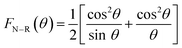 | (2) |
The variation of a (Å) on the y-axis with respect to FN–R(θ) on the x-axis is displayed in Fig. 3. The actual lattice constant a0 (Å) is estimated from the intercept of the linearly fitting data. The a0 (Å) value is found to agree well with that computed via Rietveld refinement.
 |
| | Fig. 3 Experimental lattice parameter estimated via the Nelson–Riley approach. | |
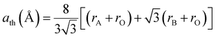
Furthermore, the theoretical unit cell parameter ath, derived from the suggested cation distribution for the analysed sample, can be expressed in terms of the ionic radii of the tetrahedral A-site rA and octahedral B-site rB as follows:29
| |
 | (3) |
where

and

,
Si designate the multiplicity of specific positions associated with element
i that exhibit ionic radii
ri residing in either a tetrahedral or an octahedral site.
rO refers to the ionic radius of oxygen, which is approximately 1.38 Å.
29 Using the generated value of
ath, we can estimate the positional oxygen parameter using the following formula:
30| |
 | (4) |
Within an undistorted cell, the ideal value of x is around 0.25. In accordance with the calculated value of x, it is plausible that the studied structure exhibits a slight distortion, which is expected in this case as a result of the structural defects.31 Furthermore, the ionic radii associated with the octahedral B-site can be expressed in terms of the positional oxygen parameter as indicated by the formula below:
| |
 | (5) |
In order to evaluate the microstructure within the studied Ni
0.4Mn
0.6Cr
2O
4 spinel chromite material, we resorted to an estimation of the average crystallite size using the well-known Size–Strain–Plot (SSP) method. This approach places less emphasis on data resulting from reflections at high angles.
32 This has a more favourable outcome for isotropic broadening, due to the fact that, at higher Bragg angles and higher diffracting, the quality of XRD data often decreases and peaks overlap. In accordance with this estimation, the profile is assumed to be represented by both a Gaussian function from the strain profile and a Lorentzian function from the crystallite size. Accordingly, the total broadening can be expressed as follows:
33βL and
βG depict peak broadening through the use of Lorentz and Gaussian functions in tandem. The (SSP) approach can be expressed as follows:
| |
 | (7) |
K and
βhkl stand for the shape factor (depending on the shape of the sample under study) and the full width at half maximum of each diffraction (
hkl) plane.
dhkl denotes the interplanar spacing, which can be expressed in terms of the Miller indices (hkl) using the following formula:
| |
 | (8) |
Eqn (7) can be graphically represented by plotting  as the ordinate with respect to
  as the abscissa (Fig. 4). By performing a linear fit of the obtained data, the slope yields the SSP crystallite size DSSP, while the intercept gives the SSP micro-strain ε.
 |
| | Fig. 4 Average crystallite size computed using the strain size plot method, inset: linear regression parameters (slope a, intercept b) and goodness-of-fit values obtained from the relation y = ax + b. | |
The Williamson–Smallman relation is employed to evaluate the length of dislocation per unit volume within an MNCO sample, which can be expressed in terms of the square crystallite size as follows:
| |
 | (9) |
Considering that the cubic spinel structure contains eight formula units per unit cell (
Z = 8), the theoretical X-ray density (
ρₓ) of the analyzed compound can be determined using the following relation:
34| |
 | (10) |
where
MW and
NA are the molecular weight and the Avogadro number, respectively. The hopping lengths between magnetic ions within tetrahedral sites (
LA−A) and octahedral sites (
LB−B) provide valuable information regarding the strength of spin interaction between ions. Both can be calculated by referring to Stanley's equation:
30| |
 | (11) |
The tetrahedral and octahedral bond lengths (dAL) and (dBL), the tetrahedral edge length (dAE), and the shared (dBE) and unshared octahedral edge lengths (dBEU) can be expressed in terms of the unit cell parameters as well as the positional oxygen parameter u:
| |
 | (12) |
| |
 | (13) |
| |
 | (14) |
| |
 | (15) |
| |
 | (16) |
The computed values of (LA−A), (LB−B), dAL, dBL, dAE, dBE and dBEU are all tabulated in Table 1. To gain a deeper insight into the structural defects within the spinel structure, a fundamental property given by the tolerance factor should be defined:
| |
 | (17) |
Table 1 Theoretical parameters computed using the Aharoni approach
| |
MSp (emu g−1) |
TtheoC (K) |
TexpC (K) |
| 0.01 T |
4.82 |
41 |
39.51 |
For an ideal spinel-structured sample, the tolerance factor is approximately unity. However, for the material under study, it is found to be equal to 0.86, suggesting the presence of a slight defect.
3.2 Electron density mapping
To gain additional evidence of the structural uniformity within the studied NMCO spinel chromite material, 3D and 2D electron density maps of the electron density (ED) distribution along the xy-plane (z = 0) inside the spinel unit cell were successfully generated via the GFourier subprogramme implemented in the FullProf Suite software package; the results are displayed in Fig. 5. According to the 3D Fourier map, the ED can be evaluated as a periodic function of position, which rises to a maximum at the exact position of an atom and drops to a minimum value in the space between atoms.35 The electron density (ED) levels are visualized in the 2D Fourier map using different contour colours. The dense and thick contours of scattered ED within the unit cell are associated with the atomic positions of heavier elements compared to lighter elements. At every point of the elementary lattice, a unique numerical value can be associated with the ED distribution, which is found to vary precisely in accordance with the spatial coordinates.36 Physically speaking, the intensity of a diffracting (hkl) plane is proportional to the square of the modulus of the atomic structure factor Fhkl defined by| |
 | (18) |
where Qhkl denotes a reciprocal space vector. The summation is extended to all atoms j in the crystalline lattice, with scattering amplitude aj and reduced coordinates xj, yj, zj. If the intensities of a sufficient number of reflections have been measured and the scattering amplitudes are known, it is conceivable that we can access the true coordinates (xj, yj, zj), thereby locating the atoms in the elementary lattice. At various lattice points in the crystal, the electron density  is given by the fast Fourier transform of the geometrical structure factor:37
| |
 | (19) |
 |
| | Fig. 5 (a) 3D electron density mapping of chromium ions. (b) 2D electron density mapping of chromium ions. (c) 3D electron density mapping of manganese (Mn) and nickel (Ni) ions. (d) 2D electron density mapping of manganese (Mn) and nickel (Ni) ions. | |
On the basis of the electron density distribution highlighted in Fig. 5(b) and (d), the thick and dense contours surrounding manganese (ZMn = 25), nickel (ZNi = 28) and chromium (ZCr = 24) indicate the distribution of 3d orbital electrons. In contrast, the lighter contours surrounding the oxygen (O) anion are mainly attributed to valence electrons within the 2p electronic sublevel. However, when talking about X-rays, it should be noted that the scattering amplitude of atoms is directly affected by the atomic number. It is therefore plausible that the heavy atoms will have a preponderant weight within the atomic structure factor. This implies that we will be capable of detecting heavy atoms with high precision, but less so for light atoms. As already observed in Fig. 5(a) and (c), Mn and Ni ions occupying the (8a) coordination sites exhibit significantly more intense ED peaks than those associated with the octahedrally coordinated Cr ions. Based on these results, manganese and nickel atoms scatter X-rays more effectively than chromium because they possess more electrons.
3.3 Magnetization study
In order to gain a deeper insight into the temperature-dependent magnetization behaviour of the studied NMCO spinel chromite sample annealed at 900 °C, typical DC thermal magnetization measurements were carried out at an external applied magnetic field of 0.01 T following zero field cooling (ZFC) and field cooling (FC) protocols, as depicted in Fig. 6. As shown in Fig. 6, the thermal variation of the ZFC and FC curves demonstrates an irreversible behaviour, which is highly informative of the presence of spin glass order within the studied structure.38 At lower temperatures, the ZFC curve increases sharply, reaching its maximum around a certain critical temperature denoted as TB. According to our plot (inset of Fig. 6), the blockage temperature is approximately 37.34 K. At around this temperature, the experimental measurement timescale is assumed to be typically within the same range as the relaxation time of the particle moments.27 The significant increase in ZFC magnetisation within this range is mainly attributable to the thermal energy (which dominates the anisotropy energy) possessed by magnetic moments. This allows them (take the liberty) to overcome the anisotropy energy barriers, thereby moving away from the easy axis direction to align with the applied magnetic field.39 The bifurcation between the FC and ZFC curves takes place around a certain critical temperature denoted as Tirr (irreversible temperature). From a physical point of view, this temperature can be associated with the blocking of the largest particles as well as the relaxation process, thereby emphasising the relationship between magnetisation and magnetic anisotropy.40 According to previous reports, the observation of both a blocking temperature (TB) and an irreversibility temperature (Tir) in the ZFC and FC magnetization curves can be primarily attributed to the distribution of magnetic anisotropy energy barriers, interparticle magnetic interactions, and particle size dispersion.41,42
 |
| | Fig. 6 FC and ZFC magnetization of Ni0.4Mn0.6Cr2O4 compound, inset: d(ZFC − FC)/dT vs. temperature. | |
The magnetic phase transition temperature, known as the Curie temperature Tc of the material under study, can be computed as follows:
✓ Experimentally, by detecting the inflection point of the plot of  with respect to T (K).
✓ Theoretically, by adjusting the thermal variation of the FC magnetization using the Aharoni approach, given by the following expression:43
| |
 | (20) |
where
MSp is associated with spontaneous magnetization and
α,
β and
γ are the model constants. The obtained experimental and theoretical results show that the studied NMCO spinel chromite compound exhibits a second-order magnetic phase transition from a ferrimagnetic state to a paramagnetic one at a specific Curie temperature of around 39 K (
Fig. 7). The theoretical value of the Curie temperature
TC, highlighted in
Table 1, was found to be significantly higher than the experimental value.
 |
| | Fig. 7 Experimental and theoretical estimation of Curie temperature TC, inset: dM/dT vs. temperature. | |
The molecular field theory of ferrimagnetism associated with nonequivalent sublattices, developed by Neel,44 provides an efficient tool for understanding how the inverse susceptibility of the investigated NMCO material behaves within the paramagnetic range (T ≫ TC). In a similar class of samples, the thermal variation of reciprocal susceptibility demonstrates a magnetic behaviour that differs from that of ferrimagnets, as well as antiferromagnets, in the higher temperature region. As a result, we observe a hyperbola instead of a straight line, and it can be estimated using the following expression:44,45
| |
 | (21) |
Here, the Curie–Weiss temperature is associated with the term

.
χ0,
δ and
θ+ are for constants. The modified Curie–Weiss law described by the previous equation can be treated as a composite of both a hyperbolic high-temperature linear part, adopting the CW form given by the first term, and a hyperbolic low-temperature asymptote indicated by the second term. In terms of the generated value of the Curie constant
C, we can express and compute the experimental effective magnetic moment
µexpeff in the paramagnetic region of the analysed NMCO sample using the following expression:
46| |
 | (22) |
where
N,
kB and
µB denote the Avogadro number, the Boltzmann constant and the Bohr magneton, respectively. In accordance with our calculations,
µexpeff was found to be equal to 7.34
µB. This experimentally measured effective magnetic moment can be compared to a theoretical one that can be calculated using the following relation:
| |
 | (23) |
herein,
µtheoeff (Mn
2+) ∼5.92
µB,
µtheoeff (Ni
2+) ∼2.83
µB and
µtheoeff (Cr
3+) ∼3.87
µB (ref.
47) denote the theoretical effective moments of divalent manganese, divalent nickel and trivalent chromium ions, respectively. The theoretical value was found to be slightly higher, reaching 7.36,
µB. When compared to
µexpeff, the theoretical effective moment per formula unit agrees well, suggesting a slightly quenched angular momentum. As a perspective, we suggest that manganese as well as nickel ions contribute significantly to the total magnetic moment. The adjusted modified Curie–Weiss parameters are tabulated in
Table 2. The thermal variation of reciprocal magnetic susceptibility is depicted in
Fig. 8.
Table 2 Adjustment modified Curie–Weiss parameters
| Applied field (Oe) |
θW (K) |
C (emu K·Oe−1·mol−1) |
δ (Oe·mol K emu−1) |
θ− (K) |
µeff (µB/f.u) |

|
| 100 |
−384 |
6.75 |
640.4 |
45.82 |
7.35 |
9.71 |
 |
| | Fig. 8 Reciprocal magnetic susceptibility adjusted by the modified Curie–Weiss law. | |
To gain deeper insight into the magnetic behaviour of our spinel NMCO chromite compound, we examined the hysteresis loop collected at an applied field of up to 8 T at a specific temperature of 5 K (as displayed in Fig. 9). At this temperature, a non-saturation behaviour was detected. Magnetization increases progressively with respect to the applied field µ0H, and does not reach the full saturation level even at the maximum field strength. From a physical point of view, two explanations were employed to account for this behaviour:48
 |
| | Fig. 9 Theoretical adjustment of the M–H hysteresis loop collected at 5 K. | |
✓ The spin disorder occurring on the nanoparticle surfaces, which is difficult to orient in the same direction as the applied magnetic field.
✓ The correlation between both ferrimagnetic and antiferromagnetic interaction processes.
In order to identify the fundamental hysteresis parameters, including Ms, HC, and Mr, and to better evaluate how the ferrimagnetic and paramagnetic contributions behave, the M–H hysteresis curve should be simulated theoretically using the following approach:48,49
| |
 | (24) |
The investigated model describes the total magnetization M(H) as the superposition of two distinct contributions: (i) a ferrimagnetic component accounted for by the arctangent term in eqn (24), which characterizes the hysteretic behavior, and (ii) a paramagnetic contribution represented by the linear term χHfH, associated with the high-field susceptibility. This latter term can be identified as forced magnetization, which occurs when spontaneous magnetization progresses linearly with respect to the applied field H.27 MFimsat, HC, ρsq and χHf denote saturation magnetisation, intrinsic coercivity, the squareness ratio  and the high field magnetic susceptibility, respectively. The coercive field is an indispensable parameter within magnetic materials. It is highly informative about the suitable applications for which the studied sample can be employed, since it can provide better insights into the ferrimagnetic nature of the investigated sample, which can be classified as soft (electromagnetic devices), semi-hard (ultra-high magnetic recording devices) or hard (permanent magnets).50,51 Furthermore, by identifying the squareness ratio ρsq, we place emphasis on the magnetic domain structure within the nanoparticles.52 On the basis of the Stoner–Wohlfarth theory,53 when ρsq is within the range of 0.2 to 0.5, the uniaxial anisotropy originates from randomly oriented multi-domain structures. Whereas, for ρsq values significantly higher than 0.5, the nanoparticles possess a mono-domain structure, therefore giving rise to anisotropic and hard materials.54 The M–H hysteresis loop of the NMCO chromite compound annealed at 900 °C, adjusted theoretically, is portrayed in Fig. 9. All the adjusted parameters are tabulated in Table 3.
Table 3 Adjusted hysteretic parameters based on the theoretical model
| Sample |
PM contribution |
FM contribution |
Percentage (%) |
| χ (emu g−1 Oe−1) |
MFimsat (emu g−1) |
HC (Oe) |
Mr (emu g−1) |
µfu (µB) |
FM |
PM |
| (5 K) |
6.09997 × 10⁻⁵ |
11.26 |
6196.03 |
8.71 |
0.45 |
58.21 |
41.79 |
In accordance with our computations, the material under study was found to exhibit a higher intrinsic coercivity of approximately 6196 Oe (493 kA m−1) at 5 K. The generated value of HC is significantly higher than 2000 Oe (159.15 kA m−1), thereby placing emphasis on the hard ferrimagnetic behaviour of our material.
As demonstrated by the following expression, the magneton number per formula unit Ni0.4Mn0.6Cr2O4 is strongly affected by its molecular weight:55
| |
 | (25) |
3.4 UV-visible/NIR spectroscopy
UV-visible/NIR spectroscopy is one of the most commonly performed analysis and characterisation techniques in several fields of research, including lasers, photoluminescence, solar cells, photovoltaics, and light-emitting diodes. This technique is particularly beneficial for quantitative measurements owing to the linear relationship that links absorbance to absorber concentration. Within molecules and inorganic samples, electrons can be promoted to higher energy levels by absorbing either incident ultraviolet or visible photons. UV-visible/NIR spectroscopy plays a significant role in both fundamental research and the technological enhancement of applied materials by enabling the examination of the optical behaviour of semiconducting compounds. Belonging to this category of compounds, various materials, including solid-state laser hosts, materials for solar cell absorbers, materials for optical information processing and ultrafast optical communication, can be analysed by UV-visible spectroscopy. In the current research, the optical properties of the studied Ni0.4Mn0.6Cr2O4 spinel chromite sample will be discussed in terms of absorbance as well as reflectivity measurements. Both are found to be highly informative regarding the optical transition mode (which may be either directly allowed or indirect), the examination of dispersive behaviour, the spectral evolution of various derived parameters (extinction coefficient k, refractive index n), and the evaluation of the band structure, thereby determining the suitable applications for which the material can be utilised.
3.4.1 Absorbance study. Using UV-visible-NIR spectrometry, the spectral behaviour of the optical absorbance and reflectivity of the NMCO compounds was investigated in the wavelength range of 190–1000 nm, as shown in Fig. 10(a) and (b). The material under study exhibits a significant, broad visible to near-infrared absorption. Therefore, demonstrating a suitable feature for visible and near-infrared optoelectronic devices.
 |
| | Fig. 10 (a) Spectral absorbance behaviour of the NMCO sample. (b) Spectral reflectance behaviour of the NMCO sample. | |
The deconvoluted absorbance spectra reveal nine absorption peaks; (i) two of which occur in the ultraviolet region (200–400 nm), (ii) six are located within the visible range (400–800 nm), and (iii) a single absorption band is in the near infrared range (800–1000 nm) (Fig. 11). The absorption band located at 243 nm mainly results from the electronic transition (t2g3)4A2g → (t2geg2)4T1g(P) associated with the trivalent chromium ion Cr3+. The highest-wavelength absorption maximum observed in the ultraviolet region at 308 nm corresponds mainly to the electronic transition from the ground state 6A1g to the 4T1g(P) state of octahedrally coordinated Mn2+.56 The first absorption band observed in the visible region occurs at 407 nm and is fundamentally associated with the d–d electronic transition 4A2g(F) → 4T1g(F) within octahedrally coordinated trivalent chromium Cr3+.57 The absorption band around 481 nm was attributable to the 6A1 → 4T1(G) electronic transition associated with the tetrahedrally coordinated divalent manganese Mn2+ ion.58 Detected at around 571 nm, the third absorption band observed in the visible range is mainly attributable to the electronic transition 3T1(3F) → 3T1(3P) that occurs within tetrahedrally coordinated Ni2+.59 Two additional bands with significantly high absorption intensities (one occurring at 632 nm) are associated with the 4A2g → 4T2g transition in octahedrally coordinated trivalent chromium Cr3+. The second, occurring at 686 nm, originates from the superposition of the spin-forbidden transition 4A2g → 2T1g, 4A2g → 2Eg of the chromium Cr3+ at the octahedral B-site.60 The last absorption band observed in the visible range, located at 751 nm, occurs mainly as a result of the d–d electronic transition within the tetrahedrally coordinated Ni2+. The only absorption band in the near infrared region is observed at around 807 nm and is attributed to the 3A2g(F) → 3T1g(P) transition in octahedrally coordinated divalent nickel Ni2+.61 As mentioned previously, the tetrahedral A-site within the normal spinel chromite is typically occupied by divalent ions (Mn2+, Ni2+), whereas the octahedral B-site is entirely occupied by Cr3+ ions due to high crystal field stabilisation energy. However, according to our interpretation, some of the octahedral B-sites are also occupied by Ni2+ and Mn2+. This suggests that divalent Ni2+ and Mn2+ ions can be distributed across both the tetrahedral A-site and the octahedral B-site. This behaviour emphasizes the antisite defect associated with the normal spinel structure and can be mainly explained by the similarity between the ionic radii of chromium and nickel.
 |
| | Fig. 11 Deconvoluted absorption spectrum of the NMCO sample. | |
3.4.2 Optical band gap energy. To provide deeper insight into the optical behaviour of the material under study, it is essential to achieve a precise estimation of its forbidden bandgap width, which is considered one of the fundamental properties of a semiconducting sample. From this perspective, it is crucial to distinguish between the optical gap and the fundamental gap. The optical gap is associated with the smallest energy transition detected within the optical absorbance spectrum, standing for the first excitation energy from the ground state to the first dipole-allowed excited state, whereas the fundamental gap can be identified by the energy difference between the first electron affinity and the first potential ionisation.62 The optical gap is typically much smaller than the fundamental gap because the electron and hole are electrostatically bound to each other in the excited state (as opposed to the ionized state).63 The optical band gap energy of the studied NMCO spinel chromite compound can be estimated using Tauc's law, given by the following formula:| |
 | (26) |
where hυ represents the incident photon energy, β is a constant factor expressing the disorder degree within the normal spinel crystal structure, and Eg is the optical band gap energy of the analysed sample. The parameter γ is a power factor associated with the electronic transition mode; it can vary depending on the semiconducting behaviour of the sample, which can be either directly allowed (γ = 1/2) or indirectly allowed (γ = 2) and prohibited. F(R∞) denotes the Kubelka–Munk function. It can be expressed in terms of the diffuse reflectance data R∞ as follows:| |
 | (27) |
where K and S correspond to the molar absorption coefficient and the scattering coefficient, respectively. By extrapolating the linear portion of  and (F(R∞)hυ)2 with respect to the incident light energy hυ, we deduce the most suitable band gap energy, which was observed when n = 1/2. Thus, for a direct band gap semiconductor sample, Tauc's law can be expressed as follows:
| | |
(F(R∞)hυ)1/2 = β(hυ − Eg)
| (28) |
The experimental estimation of the optical bandgap energy using Tauc's law is depicted in Fig. 12. To confirm the direct nature of the band gap transition, a mathematical verification can be introduced:
| | |
ln(F(R∞)hυ) = ln(β) + γln(hυ − Eg)
| (29) |
 |
| | Fig. 12 Experimental estimation of the optical bandgap energy of the NMCO sample. | |
According to the spectral dependence of ln(F(R∞)hυ) versus (hυ − Eg), the power-factor, indicating the nature of the electronic transition, is derived from the slope of the linear fit observed in Fig. 13. A linear expression can therefore be derived:
| | |
ln(F(R∞)hυ) = 3.07 + 0.5ln(hυ − 1.72)
| (30) |
 |
| | Fig. 13 Optical transition mode of the studied NMCO compound, inset: linear regression parameters (slope a, intercept b) and goodness-of-fit values obtained from the relation y = ax + b. | |
The direct band gap semiconducting behaviour was successfully verified. The experimental value of γ was found to be in very good agreement with the predicted mode. It should be noted that optoelectronic devices fabricated from direct band gap semiconducting samples are considered advantageous, since the majority of energy generated through direct recombination is emitted in the form of light without the intervention of phonons (quasi-particles associated with crystal vibrations). Optical and electronic applications can greatly benefit from the unique properties of direct band gap semiconducting materials, particularly for detectors and emitters of infrared radiation correlated with interband optical transitions.64
The forbidden bandwidth (optical band gap) and its structure in terms of the wave vector  are among the fundamental properties of a semiconducting sample and are of fundamental relevance for optoelectronic operation.65 To better analyse the band structure of the material under study, it is essential to evaluate the conduction lower edge (CB potential) and valence upper edge (VB potential), which can be calculated using the following formulas:
| |
 | (31) |
where
EC denotes the energy of the free electron on the hydrogen scale (approximately 4.5 eV) and
χ denotes the electronegativity of the studied Mn
0.6Ni
0.4Cr
2O
4 spinel chromite sample, which can be computed as follows:
| | |
χ = [χMnα χNiβ χCrδ χOτ]1/(α + β + δ + τ)
| (33) |
where
α,
β,
δ and
τ denote the multiplicity of the specific positions associated with the manganese, nickel, chromium, and oxygen ions, respectively. On the basis of the previous expressions, the computed values of
χ,
E0CB, and
E0VB were found to be equal to 5.62 eV, −0.049 eV and 1.031 eV, respectively. Thus, a descriptive scheme of the band structure can be proposed, as shown in
Fig. 14.
 |
| | Fig. 14 Band structure of the Ni0.4Mn0.6Cr2O4 sample. | |
3.4.3 Urbach energy. The investigation of the Urbach energy, denoted as EU in semiconductors, is a pivotal issue, as it plays a significant role in analysing the degree of disorder, impurities, electronic transition broadening, and structural defects (vacancies or interstitials) that result in absorption states within the region between the conduction band and the valence band, known as the Urbach tail, which can affect material properties, and consequently, their performance in applications.66,67 By evaluating the Urbach energy EU, we gain deeper insight into the tail of these localized states that extend into the bandgap on either side of the sample's forbidden bandwidth.68 The Urbach energy is highly informative about the decay length associated with the exponential tail and is inversely related to the spatial extent of the absorption states. It can be expressed in terms of the incident light energy as follows:| |
 | (34) |
By applying a Napierian logarithm to eqn (34), we obtain:| |
 | (35) |
The Urbach energy is determined by fitting the linear portion of the spectral dependence of ln (α) on the y-axis with respect to incident light energy hυ on the x-axis. It is worth noting that semiconductors with a smaller EU value are less disordered, whereas those with a higher EU value exhibit a higher density of defects and disorder. The calculated Urbach energy is approximately 0.13 eV (Fig. 15), thereby indicating a significant density of defects within the studied NMCO spinel chromite sample.
 |
| | Fig. 15 Spectral evolution of ln(α) as a function of incident photon energy. | |
Furthermore, the interaction between electrons and phonons or electrons and excitons leads to a broadening of the absorption edge. This broadening can be associated with the steepness parameter, which can be expressed in terms of the incident light energy according to the exponential Urbach law:69
| |
 | (36) |
where
kB denotes the Boltzmann constant and
EO denotes the energy of the lowest exciton state at zero lattice temperature. According to previous literature,
70 EO corresponds to
Eg in the case of direct band gap semiconductors and is equal to
Eg ±
Eph in the case of indirect band gap semiconductors (where
Eph denotes the phonon energy). Thus, by applying a Napierian logarithm on
eqn (36), we can deduce:
| |
 | (37) |
By comparing eqn (35) and (37), we can deduce
| |
 | (38) |
The steepness parameter provides insight into the rate at which the absorption coefficient changes with regard to the incident light energy near the band edge.71 In accordance with the current study, σ was estimated to be 0.19885. However, the electron–phonon interaction energy Ee–ph can be expressed in terms of the steepness of the absorption edge according to the following formula:
| |
 | (39) |
The computed value of Ee–ph was found to be equal to 3.35 eV. This parameter provides a comprehensive insight into the electronic and thermal properties of semiconductors. Semiconducting samples with a higher Ee–ph value are likely to exhibit a stronger electron–phonon interaction, indicating a greater ability to dissipate energy through lattice vibrations.
3.4.4 Linear and non-linear optical response. The study of the refractive index within semiconducting samples supplies basic information about the interaction between incident electromagnetic waves and matter. It plays a substantial role in selecting specific semiconductors for the design of optoelectronic devices, including optical switches, modulators, and filters. When irradiated by an incident electromagnetic wave, a semiconducting material exhibits a variable refractive index that depends on the wavelength of the incident radiation. Physically speaking, the complex refractive index is regarded as a combination of two contributions; one of which is described by the real part, whereas the other is expressed by an imaginary number:72| |
![[n with combining circumflex]](https://www.rsc.org/images/entities/i_char_006e_0302.gif) = n(λ) + ik(λ) = n(λ) + ik(λ)
| (40) |
The real part, denoted as n(λ) is associated with the optical refractive index. It provides insight into the local field as well as the electronic polarization of ions inside semiconductors,73 while the imaginary part, denoted as k(λ), refers to the extinction coefficient. The latter is highly informative about the attenuation of incident electromagnetic waves as they propagate through matter.74 Both parameters can be expressed using the following Kramer–Kronig formulas:75
| |
 | (41) |
| |
 | (42) |
The spectral dependences of the extinction coefficient and the refractive index with respect to the incident radiation wavelength are depicted in Fig. 16 and 17, respectively. It can be observed from Fig. 16 that k exhibits a value much lower than unity. Furthermore, in the wavelength range of 190–681 nm, the extinction coefficient increases and exhibits higher values, suggesting greater light loss in this region. In contrast, within the remaining spectral range (681–1000 nm), k drastically decreases to reach its minimum value, highlighting the significant transmission within this region. This suggests that the studied sample can be considered a highly transparent compound in this range. According to the spectral evolution of n as a function of incident wavelength radiation, one can observe that n increases markedly as wavelength increases, emphasising the decrease in light velocity during propagation through the sample. The spectral behaviour of the real part of the refractive index can be modelled using the Cauchy dispersion function, given by the following expression:
| |
 | (43) |
where
n0 denotes the static refractive index. The theoretical adjustment of
n by using the Cauchy model is depicted in the inset of
Fig. 17.
 |
| | Fig. 16 Spectral evolution of extinction coefficient with respect to wavelength. | |
 |
| | Fig. 17 Spectral evolution of refractive index n vs. l, inset: theoretical adjustment of n by using the Cauchy model. | |
Accordingly, by using the generated value of the static refractive index, we can estimate the reflection loss factor using the following relation:
| |
 | (44) |
The reflection loss value of the studied MNCO spinel chromite compound was estimated to be 0.063. Furthermore, structural imperfections, which can disrupt the periodicity of electronic charge density, can occur even within perfect lattices.76 This phenomenon is basically ascribed to the interaction between charge carriers (electrons or holes) and lattice ion vibrations, thus leading to the formation of quasiparticles known as ‘polarons’.77 In particular, the excess charge displaces neighbouring ions as a result of Coulomb interactions, thus creating a polarization cloud that tracks the charge carrier as it moves through the crystal.76 Polaron creation is especially advantageous in polar semiconducting samples and metallic oxides due to their strong electron–phonon interaction; it is even more favoured at surfaces where the crystal lattice is more flexible and lattice relaxations require less energy.78,79 The polaron radius can be computed using the following expression:
| |
 | (45) |
Herein, N stands for the number of crystallographic sites per unit volume. Based on the crystallographic structure associated with normal spinel symmetry, which consists of 32 octahedral sites and 64 tetrahedral sites, N is found to be equal to 96/a3 (where a denotes the unit cell parameter).
The molar refractive index denoted as Rm of the material under study can be expressed in terms of the refractive index n and the molar volume Vm according to the Lorentz–Lorenz formula:
| |
 | (46) |
Accordingly, by assuming that  , we obtain
| |
 | (47) |
An additional parameter, known as the molar electronic polarizability αm, can be expressed in terms of the molar refractive index Rm based on the following expression:
| |
 | (48) |
where
NA corresponds to Avogadro's number (
NA = 6.023 × 10
23 mol
−1). The computed values of the polaron radius, molar refractive index and molar electronic polarizability are listed in
Table 4. It should be noted that the polarizability factor provides insight into a semiconductor's ability to induce an electric dipole moment after being subjected to an external electromagnetic field, responding to the incident electromagnetic field by shifting its charge carriers. In addition, the current study demonstrates a direct proportionality between molar refraction and molar electronic polarizability. This proportionality is useful when investigating the optical non-linear response since it is dependent on electronic polarizability.
Table 4 Computed optical parameters of Ni0.4Mn0.6Cr2O4
| Sample |
Ni0.4Mn0.6Cr2O4 |
| Oscillator energy E0 (eV) |
7.62 |
| Dispersion energy Ed (eV) |
11.75 |
| Oscillator wavelength (nm) |
162.747 |
| Average oscillator strength (10−5 nm−2) |
5.82 |
| Transition moment M(−1) (eV) |
1.54 |
| Transition moment M(−3) (eV−2) |
0.026 |
| Oscillator strength (eV2) |
89.53 |
| Static refractive index |
1.59 |
| Static dielectric constant |
2.54 |
| χ(3) (10−22 m2 V−2) |
1.46 |
| n2 (10−22 m2 V−2) |
3.46 |
| RL |
0.062 |
| Rp (Å) |
0.35 |
| Rm (cm3 mol−1) |
20.97 |
| αm (Å3) |
8.31 |
Regarding the dispersive behaviour of the studied MNCO material, it is relevant to study the single effective oscillator model developed by Wemple–DiDomenico.80 The dispersion of the optical refractive index within a semiconducting sample plays a significant role in the design of optoelectronic devices and optical communication systems.81 The common practice for insulating and semiconducting samples involves identifying an inverse correlation between the characteristic interband energy and the optical refractive index. In particular, this correlation is found to be highly effective in semiconducting materials, and it can be extended to an analogous correlation with the optical band-gap energy.82
The primary outcome of the theoretical Wemple–DiDomenico approach is the dispersive energy, denoted as Ed. This parameter can be associated with the coordination number of samples and valence ionicity.83 It provides significant insight into the strength of inter-band optical transitions. Furthermore, the single oscillator energy given by E0 is highly informative about the average excitation energy required for electronic transitions.84 Both parameters can be expressed in terms of the incident light frequency and refractive index as follows:
| |
 | (49) |
where h is the Planck constant (around 6.62 × 10
−34 J s
−1). By fitting the linear portion of the spectral evolution of (
n2 − 1)
−1 with respect to the square of incident light energy, one can determine
Ed and
E0 from the slope and intercept values, as shown in
Fig. 18. According to the Sellmeier single-oscillator model, another result can be identified by computing the oscillator strength
S0 as well as the oscillator wavelength
λ0. These parameters can be correlated to the optical refractive index according to the following expression:
85| |
 | (50) |
By fitting the linear portion of the evolution of (
n2 − 1)
−1 with respect to the reciprocal of the square of the wavelength, one can estimate
S0 and
λ0 using the slope and
y-axis intercept values, as depicted in
Fig. 19.
 |
| | Fig. 18 Evolution of (n2 − 1)−1 with respect to the square of incident photon energy. | |
 |
| | Fig. 19 Evolution of (n2 − 1)−1 with respect to the reciprocal square wavelength. | |
Furthermore, in the low-frequency region, the static refractive index as well as the zero-frequency dielectric constant can be estimated by referring to the computed values of E0 and Ed:86
| |
 | (51) |
The computed low-frequency static refractive index was found to be in very good agreement with that estimated using the theoretical Cauchy model. This agreement places emphasis on the accuracy and reliability of the results achieved through these various approaches. Using the obtained values of the single oscillator parameters, we computed the moments M(−1) and M(−3), as explained by the following equations:
| |
 | (52) |
| |
 | (53) |
The oscillator strength is directly connected to the dispersion parameters E0 and Ed and can be expressed as follows:
The computed values of the single effective oscillator parameters for the studied NMCO compound are summarized in Table 4 and Fig. 20.
 |
| | Fig. 20 Spectral behaviour of linear optical susceptibility. | |
Optical nonlinearity (ONL) is a major field that has grown exponentially over the last few years owing to its multitude of applications in novel photonic effects. Nonlinear optics provides a deeper insight into both elastic and inelastic light scattering phenomena when intense light radiation interacts with a sample composed of molecules or atoms.87 Optical nonlinearity manifests when an external electric field  induces a non-harmonic displacement of the charge carriers (electrons) within a compound (composed of nanoparticles). The induced electric dipole moments, which oscillate at the same frequency as the applied electric field, sum up, leading to the generation of macroscopic polarisation in the irradiated material. In fact, while smaller expansion coefficients render higher-order nonlinearities of little interest in some cases, they can still be significant when resonantly enhanced in matter.87 The macroscopic polarizability can therefore be expressed in terms of the electric field strength according to the following formula:88
| | |
P = ε0[χ(1)E + χ(2)E2 + χ(3)E3 + …]
| (55) |
where
ε0 denotes the dielectric permittivity of free space (
ε0 = 8.854 × 10
−12 F m
−1). The term
χ(1) is associated with the linear susceptibility, whereas the second-order nonlinear optical susceptibility and third-order nonlinear susceptibility are denoted as
χ(2) and
χ(3), respectively. A clear connection between the linear susceptibility and the refractive index is based on the following expression:
| |
 | (56) |
The spectral behaviour of the linear susceptibility with respect to the incident light wavelength is depicted in Fig. 21. Accordingly, the third-order nonlinear susceptibility χ(3) can be anticipated based on the linear susceptibility as follows:
| |
 | (57) |
Here,
A is associated with a constant parameter estimated to be approximately 1.7 × 10
−10 esu (where 1 esu is equivalent to 1.4 × 10
−8 m
2 V
−2). The evolution of the third-order nonlinear susceptibility
χ(3) with respect to the incident radiation wavelength is displayed in
Fig. 21. In the low-energy region, the quadratic susceptibility can be expressed in terms of
E0 as well as
Ed as follows:
89| |
 | (58) |
 |
| | Fig. 21 Spectral evolution of the third-order non-linear optical susceptibility. | |
The nonlinear refractive index can be expressed in terms of the static refractive index and the quadratic susceptibility by referring to the subsequent formula:90
| |
 | (59) |
The calculated values of χ(1), χ(3) and n2 (tabulated in Table 4) were found to be in very good agreement with those of other compounds considered suitable for nonlinear applications, including ultrafast optical communication and optical information processing.
3.4.5 Optical and electric conductivity. The investigation of conductivity within a semiconducting sample can be achieved by evaluating two types of contributions: electrical and optical conductivities. The first provides insight into the charge carrier (electrons and holes) transport phenomena, while the second is directly connected to the electron–photon interaction mechanism. It should be noted that the exponential evolution of conductivity within semiconductors is typically influenced by temperature and forbidden bandwidth. Charge carriers that are responsible for conductivity in similar materials are either positive holes, electrons or ions.72 In terms of the optical absorption coefficient, the two conductivity contributions can be expressed as:91| |
 | (60) |
| |
 | (61) |
where C is the velocity of light in vacuum (approximately 3 × 10⁸ m s−1). The plots of optical and electrical conductivity with respect to the incident light radiation are illustrated in Fig. 22 and 23. The higher optical conductivity values observed within the high absorption range are mainly attributed to the excited free charges that have successfully crossed the forbidden bandgap thanks to the higher photon absorption rates, placing therefore emphasis on the significant potential of our material to interact with incident light at these regions.92 On the other hand, the lower values of electrical conductivity compared to those of optical conductivity are mainly attributed to the electrons that have not succeeded to cross the potential barrier levels.
 |
| | Fig. 22 Spectral evolution of the optical conductivity of the NMCO compound. | |
 |
| | Fig. 23 Spectral evolution of the electrical conductivity of the NMCO compound. | |
3.4.6 Optical dielectric constant. The study of optical dielectric constants within semiconducting materials is of great interest since it provides significant information for the design of high-performance optoelectronic devices. The optical dielectric constant is a complex function comprising two contributions: the real part, which provides insight into the refraction of light as it propagates through matter, and the imaginary part, which describes the attenuation of incident radiation waves. Both components can be expressed in terms of the refractive index and the extinction coefficient as follows:| | |
εr(λ) = n2(λ) − k2(λ)
| (62) |
In accordance with the spectral evolution of the real and imaginary parts of the dielectric permittivity with respect to the incident radiation energy, as illustrated in Fig. 24, it can be seen that the real part εr(λ) shows a similar trend to the refractive index, which, in turn, behaves similarly to the reflectance. Furthermore, the imaginary part of the dielectric constant exhibits a behaviour similar to that of the extinction coefficient kkk, which is directly influenced by the optical absorbance of the material. The dielectric loss, also known as the dissipation factor tan(δ), represents the amount of electrical energy that is dissipated as heat within semiconducting materials. It corresponds to the ratio between the imaginary and real parts of the dielectric constant:| |
 | (64) |
 |
| | Fig. 24 Spectral evolution of the real (blue) and imaginary (red) parts of the optical dielectric constant. | |
The plot of the dissipation loss factor tan(δ) with respect to incident radiation energy is depicted in Fig. 25. As a matter of fact, the spectral behaviour of tan(δ) reveals small values for the dissipation loss factor, thereby emphasising the low dissipation rate of light that propagates through our material. Furthermore, Fig. 25 depicts a significant increase within the spectral range between 1.25 and 1.83 eV, suggesting that activation levels occur in this region.
 |
| | Fig. 25 Spectral evolution of dielectric loss as a function of incident photon energy. | |
4 Conclusion
In sum, spinel chromite Ni0.4Mn0.6Cr2O4 has been successfully synthesised via the sol–gel method. The structural refinement by the Rietveld method reveals the formation of a pure phase of Ni-based spinel chromite, which crystallises according to the cubic system with the (Fdm) space group. The average crystallite size estimated using the strain size plot (SSP) was found to be 96.54 nm. The magnetic investigation reveals a transition from paramagnetic to hard ferrimagnetic behaviour at 39 K. The significant coercivity observed at low temperatures, rooted in the electronic anisotropy evidenced by density mapping, suggests the compound's potential for low-temperature hard chromite applications.
Furthermore, the bandgap (Eg) and Urbach (Eu) energies were found to be lower for the NMCO sample. A comprehensive analysis of various optical parameters, including refractive index, penetration depth, extinction coefficients, nonlinear optical parameters, optical conductivity, and dielectric constants, was also presented. Our findings indicate that the substitution of Mn2+ ions in nickel chromites (NiCr2O4) enhances their visible-light absorption. The NMCO sample demonstrates significant advantages, including easy and cost-effective synthesis, lower band gap energy, good transparency, efficient light absorption, and effective energy conversion. These materials hold potential for various optoelectronic fields, including solar cells and photocatalysis.
Future research will focus on expanding this compositional series to further refine the structure–property relationships. Specifically, investigating electrical conductivity and implementing strategic doping or surface modifications will be essential to optimize these chromites for next-generation optoelectronic and microwave absorption technologies. This work provides the fundamental framework necessary for the integration of Mn–Ni chromites into high-performance technological applications.
Conflicts of interest
There are no conflicts to declare.
Data availability
Data are available from the authors upon request.
Supplementary information (SI): Table SI1 summarizes the structural parameters obtained from the Rietveld refinement, including the crystal structure, space group, lattice parameters, atomic positions, and reliability (agreement) factors. See DOI: https://doi.org/10.1039/d5ra10066f.
Acknowledgements
This work was supported by the Tunisian Ministry of Higher Education, Scientific Research, and Technology for its funding through the excellence project code : P2ES2025-D6P1.
References
- K. Vanasundari, G. Mahalakshmi and A. Prakasam, Impact of Mg 2+ substitution on the band gap energy, urbach energy, structure, and optical behavior of copper chromites nanoparticles, Next Mater., 2024, 4, 100196, DOI:10.1016/j.nxmate.2024.100196.
- V. H. Choudapur, V. J. Angadi, N. H. Ayachit, M. Ubaidullah and B. Pandit, Role of 5 mol% rare earth (La3+) on the structural, microstructural, and magnetic properties of cobalt chromite ceramics, Ceram. Int., 2023, 49, 33944–33951, DOI:10.1016/j.ceramint.2023.08.089.
- O. Chouikhi and R. Masrour, Study of structural, electronic, thermodynamic, thermoelectric, and optical properties of superconductor spinel LiTi2O4: An ab initio calculations, J. Power Sources, 2025, 634, 236453, DOI:10.1016/j.jpowsour.2025.236453.
- M. Liu, H. Su, K. Song, R. Wang, X. Li, L. Hu, X. Lv and Y. Xin, Thermodynamic data of a promising magnetic material MnCr2O4 and thermodynamic analysis of its application process, Calphad, 2024, 87, 102728, DOI:10.1016/j.calphad.2024.102728.
- S. Akhtar, A. Hussain, S. Noreen, N. Bibi, M. Bilal Tahir and J. Ur Rehman, A comparative DFT study of MgFe2O4 and MnFe2O4 spinel ferrites at various pressures to investigate the structural, mechanical, electronic, magnetic and optical properties for multifunctional applications, Comput. Theor. Chem., 2024, 1235, 114546, DOI:10.1016/j.comptc.2024.114546.
- X. Xu, J. Gao and W. Hong, Ni-based chromite spinel for high-performance supercapacitors, RSC Adv., 2016, 6, 29646–29653, 10.1039/C5RA27931C.
- M. M. Rahman, H. A. Miran, Z.-T. Jiang, M. Altarawneh, L. S. Chuah, H.-L. Lee, A. Amri, N. Mondinos and B. Z. Dlugogorski, Investigation of the post-annealing electromagnetic response of Cu–Co oxide coatings via optical measurement and computational modelling, RSC Adv., 2017, 7, 16826–16835, 10.1039/C6RA25626K.
- F. Iacomi, G. Calin, C. Scarlat, M. Irimia, C. Doroftei, M. Dobromir, G. G. Rusu, N. Iftimie and A. V. Sandu, Functional properties of nickel cobalt oxide thin films, Thin Solid Films, 2011, 520, 651–655, DOI:10.1016/j.tsf.2011.08.067.
- Y. Sahu and S. Agrawal, Effect of Fe3+ ions substitution on electrical and dielectric properties of MgFexCr2-xO4 (x = 0, 0.2, and 0.4 mol%) chromites prepared by solution combustion method, Chem. Phys. Impact, 2024, 8, 100655, DOI:10.1016/j.chphi.2024.100655.
- D. Harrabi, S. Hcini, I. Ghiloufi, A. Mimouni, J. Dhahri and K. Khirouni, Studies of the microstructural, magnetic, electrical, and dielectric properties of Mg0.6T0.4Cr2O4 (T = Ni, Cu) spinel chromites for magnetic, high frequency, and microwave applications, J. Magn. Magn. Mater., 2023, 582, 171040, DOI:10.1016/j.jmmm.2023.171040.
- A. B. A. Hajji, M. Wali, R. Dhahri, E. Dhahri, J. F. M. L. Mariano and M. Jemmali, A comprehensive study of the structural, magnetic and optoelectronic behavior of Ni0.6Mn0.4Cr2O4 chromite for magneto optical devices, Ceram. Int., 2025, S0272884225007163, DOI:10.1016/j.ceramint.2025.02.050.
- N. M. Khalil, M. B. Hassan, E. M. M. Ewais and F. A. Saleh, Sintering, mechanical and refractory properties of MA spinel prepared via co-precipitation and sol–gel techniques, J. Alloys Compd., 2010, 496, 600–607, DOI:10.1016/j.jallcom.2010.02.123.
- M. I. A. A. Maksoud, G. S. El-Sayyad, A. H. Ashour, A. I. El-Batal, M. A. Elsayed, M. Gobara, A. M. El-Khawaga, E. K. Abdel-Khalek and M. M. El-Okr, Antibacterial, antibiofilm, and photocatalytic activities of metals-substituted spinel cobalt ferrite nanoparticles, Microb. Pathog., 2019, 127, 144–158, DOI:10.1016/j.micpath.2018.11.045.
- Y. Youn, J. Miller, K. Nwe, K.-J. Hwang, C. Choi, Y. Kim and S. Jin, Effects of Metal Dopings on CuCr2 O4 Pigment for Use in Concentrated Solar Power Solar Selective Coatings, ACS Appl. Energy Mater., 2019, 2, 882–888, DOI:10.1021/acsaem.8b01976.
- Y. El Jabbar, H. Lakhlifi, R. El Ouatib, L. Er-Rakho, S. Guillemet-Fritsch and B. Durand, Preparation and characterisation of green nano-sized ceramic pigments with the spinel structure AB2O4 (A = Co, Ni and B = Cr, Al), Solid State Commun., 2021, 334–335, 114394, DOI:10.1016/j.ssc.2021.114394.
- C. L. Li, T. Y. Yan, G. O. Barasa, Y. H. Li, R. Zhang, Q. S. Fu, X. H. Chen and S. L. Yuan, Negative magnetization and exchange bias effect in Fe-doped CoCr2O4, Ceram. Int., 2018, 44, 15446–15452, DOI:10.1016/j.ceramint.2018.05.200.
- W. Xu, G. Lin, M. Shu, J. Jiao, J. Zhu, Q. Ren, M. D. Le, X. Luo, Y. Sun, Y. Liu, Z. Qu, H. Zhou, S. Gao and J. Ma, Spin Dynamics and Phonons in Chromites CoCr2 O4 and MnCr2 O4, Chin. Phys. Lett., 2024, 41, 117503, DOI:10.1088/0256-307X/41/11/117503.
- G. C. Pandey, D. Gangwar, H. Tripathi, G. Aquilanti and C. Rath, Crystal structure, local structure and magnetic properties of NiCr2-Fe O4 (x = 0.3–0.6) spinel, Mater. Chem. Phys., 2021, 271, 124861, DOI:10.1016/j.matchemphys.2021.124861.
- K. Vanasundari, A. Viji, R. Vijayakumar and A. Prakasam, NiCr2−xGdxO4 ceramics' magnetic, structural and electrical conductivity as well as their activation energy properties, Inorg. Chem. Commun., 2024, 170, 113110, DOI:10.1016/j.inoche.2024.113110.
- A. Ajith, T. A. Wani, G. Suresh, N. Saravanan and R. Masrour, Sol–Gel Synthesis and Characterizations of Spinel Nickel Chromite (NiCr2 O4) Nanoparticles to Study their Photocatalytic, Antibacterial and Anticancer Activities, NANO, 2024, 19, 2450050, DOI:10.1142/S1793292024500504.
- K. Mahi, K. El Assad Zemallach Ouari, R. Mostefa and M. Trari, Synthesis, characterization, and optical properties of NiCr2 O4 and CoCr2 O4 spinel nanostructures for photocatalytic applications, Eur. Phys. J.:Appl. Phys., 2025, 100, 2, DOI:10.1051/epjap/2024026.
- A. Abbasi, H. Khojasteh, A. H. Keihan, K. Adib, A. Sobhani-Nasab and M. Rahimi-Nasrabadi, Co-precipitation synthesis of Ag-doped NiCr2O4 nanoparticles: investigation of structural, optical, magnetic, and photocatalytic properties, J. Mater. Sci.: Mater. Electron., 2021, 32, 1413–1426, DOI:10.1007/s10854-020-04913-3.
- M. A. Kassem, A. A. El-Fadl, A. M. Nashaat, and H. Nakamura, Structural, Optical and Single-Domain Magnetic Features of the Noncollinear Ferrimagnetic Nano-Spinel Chromites ACr$_2$O$_4$ (A = Ni, Co, and Mn), 2023, DOI:10.48550/ARXIV.2305.17856.
- A. M. Nashaat, M. A. Kassem, A. Abu El-Fadl and H. Nakamura, Low-temperature cluster spin glass transition in the single-domain NiCr2 O4 nanoparticles, Nanotechnology, 2024, 35, 195702, DOI:10.1088/1361-6528/ad2453.
- M. Saeed, M. Rani, K. Batool, H. Batool, A. Younus, S. Azam, A. Mehmood, B. Haq, T. Alshahrani, G. Ali and M. Maqbool, Synthesis and Fabrication of Co1−xNixCr2O4 Chromate Nanoparticles and the Effect of Ni Concentration on Their Bandgap, Structure, and Optical Properties, J. Compos. Sci., 2021, 5, 247, DOI:10.3390/jcs5090247.
- A. Abbasi, S. M. S. Sajadi, O. Amiri, M. Hamadanian, H. Moayedi, M. Salavati-Niasari and M. M. Beigi, MgCr2O4 and MgCr2O4/Ag nanostructures: Facile size-controlled synthesis and their photocatalytic performance for destruction of organic contaminants, Composites, Part B, 2019, 175, 107077, DOI:10.1016/j.compositesb.2019.107077.
- S. K. Paswan, S. Kumari, M. Kar, A. Singh, H. Pathak, J. P. Borah and L. Kumar, Optimization of structure-property relationships in nickel ferrite nanoparticles annealed at different temperature, J. Phys. Chem. Solids, 2021, 151, 109928, DOI:10.1016/j.jpcs.2020.109928.
- M. Verma, M. B. Newmai and P. Senthil Kumar, Synergistic effect of Au–Ag nano-alloying: intense SEIRA and enhanced catalysis, Dalton Trans., 2017, 46, 9664–9677, 10.1039/C7DT02130E.
- T. Tatarchuk, A. Shyichuk, I. Trawczyńska, I. Yaremiy, A. T. Pędziwiatr, P. Kurzydło, B. F. Bogacz and R. Gargula, Spinel cobalt(II) ferrite-chromites as catalysts for H2O2 decomposition: Synthesis, morphology, cation distribution and antistructure model of active centers formation, Ceram. Int., 2020, 46, 27517–27530, DOI:10.1016/j.ceramint.2020.07.243.
- M. A. Islam, A. K. M. A. Hossain, M. Z. Ahsan, M. A. A. Bally, M. S. Ullah, S. M. Hoque and F. A. Khan, Structural characteristics, cation distribution, and elastic properties of Cr3+ substituted stoichiometric and non-stoichiometric cobalt ferrites, RSC Adv., 2022, 12, 8502–8519, 10.1039/D1RA09090A.
- H. L. Andersen, M. Saura-Múzquiz, C. Granados-Miralles, E. Canévet, N. Lock and M. Christensen, Crystalline and magnetic structure–property relationship in spinel ferrite nanoparticles, Nanoscale, 2018, 10, 14902–14914, 10.1039/C8NR01534A.
- M. Rabiei, A. Palevicius, A. Monshi, S. Nasiri, A. Vilkauskas and G. Janusas, Comparing Methods for Calculating Nano Crystal Size of Natural Hydroxyapatite Using X-Ray Diffraction, Nanomaterials, 2020, 10, 1627, DOI:10.3390/nano10091627.
- J. F. Nye, Physical Properties of Crystals: Their Representation by Tensors and Matrices, Reprinted, Clarendon Press, Oxford, 2012 Search PubMed.
- D. Gherca, A. Pui, N. Cornei, A. Cojocariu, V. Nica and O. Caltun, Synthesis, characterization and magnetic properties of MFe2O4 (M=Co, Mg, Mn, Ni) nanoparticles using ricin oil as capping agent, J. Magn. Magn. Mater., 2012, 324, 3906–3911, DOI:10.1016/j.jmmm.2012.06.027.
- K. Dubey, S. Dubey, V. Sahu, R. A. Parry, A. Modi and N. K. Gaur, Structural, optical and magnetic properties of CoFe2O4 nanoparticle synthesized by ultrasonication-assisted sol–gel technique, Appl. Phys. A, 2022, 128, 560, DOI:10.1007/s00339-022-05681-z.
- A. Kumari, O. Singh, E. Arya, M. Chauhan, V. Vermani, S. Sanghi and A. Agarwal, Crystal structure, dielectric and magnetic properties of (1 −x)BaTiO3-(x)BaFe12O19 (x = 0.50, 0.60, 0.70) multiferroic composites, Appl. Phys. A, 2023, 129, 334, DOI:10.1007/s00339-023-06596-z.
- O. Singh, A. Agarwal, S. Sanghi and J. Singh, Variation of crystal structure, magnetization, and dielectric properties of Nd and Ba co-doped BiFeO3 multiferroics, Int. J. Appl. Ceram. Technol., 2019, 16, 119–129, DOI:10.1111/ijac.13052.
- R. Hamdi, M. Smari, A. Bajorek, L. Bessais, Y. Haik, E. Dhahri and S. Hayek, Large magnetocaloric entropy change in ferrimagnetic Er1-xCo2 systems at cryogenic temperatures: the role of erbium deficiency, Appl. Phys. A, 2021, 127, 39, DOI:10.1007/s00339-020-04147-4.
- S. Kumari, V. Kumar, P. Kumar, M. Kar and L. Kumar, Structural and magnetic properties of nanocrystalline yttrium substituted cobalt ferrite synthesized by the citrate precursor technique, Adv. Powder Technol., 2015, 26, 213–223, DOI:10.1016/j.apt.2014.10.002.
- C. Cannas, A. Musinu, G. Piccaluga, D. Fiorani, D. Peddis, H. K. Rasmussen and S. Mørup, Magnetic properties of cobalt ferrite–silica nanocomposites prepared by a sol-gel autocombustion technique, J. Chem. Phys., 2006, 125, 164714, DOI:10.1063/1.2354475.
- S. Mallesh, V. Srinivas, M. Vasundhara and K. H. Kim, Low-temperature magnetization behaviors of superparamagnetic MnZn ferrites nanoparticles, Phys. B, 2020, 582, 411963, DOI:10.1016/j.physb.2019.411963.
- R. N. Bhowmik and K. S. Aneeshkumar, Low temperature ferromagnetic properties, magnetic field induced spin order and random spin freezing effect in Ni1.5Fe1.5O4 ferrite; prepared at different pH values and annealing temperatures, J. Magn. Magn. Mater., 2018, 460, 177–187, DOI:10.1016/j.jmmm.2018.04.001.
- A. Aharoni, Introduction to the Theory of Ferromagnetism, 2nd edn, Oxford University Press, Oxford; New York, 2000 Search PubMed.
- J. S. Smart, The Néel Theory of Ferrimagnetism, Am. J. Phys., 1955, 23, 356–370, DOI:10.1119/1.1934006.
- B. D. Cullity, and C. D. Graham, Introduction to Magnetic Materials, 2nd edn, IEEE/Wiley, Hoboken, New Jersey, 2015 Search PubMed.
- F. Hcini, S. Hcini, M. M. Almoneef, M. H. Dhaou, M. S. Alshammari, A. Mallah, S. Zemni, N. Lefi and M. L. Bouazizi, Thermal, microstructural, optical, magnetic and magnetocaloric studies for Ni0.5Mn0.5Cr2O4 chromite spinel prepared using sol-gel method, J. Mol. Struct., 2021, 1243, 130769, DOI:10.1016/j.molstruc.2021.130769.
- Y. Gao, H. Chang, Q. Wu, H. Wang, Y. Pang, F. Liu, H. Zhu and Y. Yun, Optical properties and magnetic properties of antisite-disordered Ni 1–x Co x Cr 2 O 4 spinels, Trans. Nonferrous Met. Soc. China, 2017, 27, 863–867, DOI:10.1016/S1003-6326(17)60099-2.
- S. B. Amor, A. Benali, M. Bejar, E. Dhahri, K. Khirouni, M. A. Valente, M. P. F. Graça, F. Al-Turjman, J. Rodriguez and A. Radwan, Modulation of magnetism and study of impedance and alternating current conductivity of Zn0.4Ni0.6Fe2O4 spinel ferrite, J. Mol. Struct., 2019, 1184, 298–304, DOI:10.1016/j.molstruc.2019.02.053.
- A. E. Mabrouki, O. Messaoudi and L. H. Alfhaid, Synthesis and Investigation of Optical, Magnetic, and Thermoelectric Properties of Li0.5 Zr0.5 Mg0.5 Fe1.5 O4 Spinel and First-Principles Characterization as an Electrode Material for Li-Ion Batteries, Cryst. Growth Des., 2023, 23, 6526–6534, DOI:10.1021/acs.cgd.3c00487.
- J. M. D. Coey, Perspective and Prospects for Rare Earth Permanent Magnets, Engineering, 2020, 6, 119–131, DOI:10.1016/j.eng.2018.11.034.
- L. Bessais, Structure and Magnetic Properties of Intermetallic Rare-Earth-Transition-Metal Compounds: A Review, Materials, 2021, 15, 201, DOI:10.3390/ma15010201.
- X. Yu, N. Zhou, R. Liu, L. Wang, Z. Xu, H. Gong, T. Zhao, J. Sun, F. Hu and B. Shen, Effect of Zn2+-Sn4+ co-substitution on structural and magnetic properties of SrFe12-2xZnxSnxO19 (x = 0–2) M-type strontium ferrite, Phys. B, 2023, 653, 414676, DOI:10.1016/j.physb.2023.414676.
- E. P. Wohlfarth, Relations between Different Modes of Acquisition of the Remanent Magnetization of Ferromagnetic Particles, J. Appl. Phys., 1958, 29, 595–596, DOI:10.1063/1.1723232.
- C. C. Chauhan, A. R. Kagdi, R. B. Jotania, A. Upadhyay, C. S. Sandhu, S. E. Shirsath and S. S. Meena, Structural, magnetic and dielectric properties of Co-Zr substituted M-type calcium hexagonal ferrite nanoparticles in the presence of α-Fe2O3 phase, Ceram. Int., 2018, 44, 17812–17823, DOI:10.1016/j.ceramint.2018.06.249.
- Y. Marouani, A. Mabrouki, R. Dhahri, E. Dhahri and B. F. O. Costa, Experimental and theoretical studies of structural, magnetic and electronic properties of Ba1-xSrxFe12O19 (x = 0, 0.5, 1) hexaferrites, Inorg. Chem. Commun., 2022, 136, 109163, DOI:10.1016/j.inoche.2021.109163.
- P. Koidl and K. W. Blazey, Optical absorption of MgO:Mn, J. Phys. C: Solid State Phys., 1976, 9, L167–L170, DOI:10.1088/0022-3719/9/6/008.
- A. E. Shaker, H. Y. Morshidy, M. A. Hassan and I. M. El-Kashef, Effect of 3d-transition metal ions on the structural, optical and magnetic properties of chromium-bearing barium borate glass, Ceram. Int., 2024, 50, 1879–1890, DOI:10.1016/j.ceramint.2023.10.289.
- S. Pitula and A. Mudring, Synthesis, Structure, and Physico-optical Properties of Manganate(II)-Based Ionic Liquids, Chem.–Eur. J., 2010, 16, 3355–3365, DOI:10.1002/chem.200802660.
- B. Johnson, N. R. K. Chand, B. K. Sudhakar and G. Srinivasa Rao, Chemical durability, thermal stability and spectroscopic studies of the influence of Ni2+ ions in oxyfluorophosphate glasses, J. Mater. Sci.: Mater. Electron., 2016, 27, 8833–8847, DOI:10.1007/s10854-016-4909-3.
- I. Kashif and A. Ratep, Optical properties of borate glasses containing chromium and erbium oxide, Appl. Phys. A, 2023, 129, 489, DOI:10.1007/s00339-023-06764-1.
- N. A. M. Alsaif, H. Al-Ghamdi, A. M. El-Refaey, M. S. Sadeq, M. S. Shams, S. M. Shaaban, Y. I. Mesalam, E. M. Ahmed, Y. S. Rammah, A. I. Salem and R. A. Elsad, Synthesis, structural, optical properties and dielectric spectroscopy of nickel-doped lead borate glasses, Opt. Quantum Electron., 2024, 56, 383, DOI:10.1007/s11082-023-06059-y.
- J. Zirzlmeier, S. Schrettl, J. C. Brauer, E. Contal, L. Vannay, É. Brémond, E. Jahnke, D. M. Guldi, C. Corminboeuf, R. R. Tykwinski and H. Frauenrath, Optical gap and fundamental gap of oligoynes and carbyne, Nat. Commun., 2020, 11, 4797, DOI:10.1038/s41467-020-18496-4.
- J.-L. Bredas, Mind the gap, Mater. Horiz., 2014, 1, 17–19, 10.1039/C3MH00098B.
- C. R. Pidgeon, SEMICONDUCTOR MATERIALS | Band Structure Engineering, in Encyclopedia of Modern Optics, Elsevier, 2005, pp. 347–351, DOI:10.1016/B0-12-369395-0/00621-7.
- T. Markvart, and L. Castañer, Semiconductor Materials and Modelling, in Solar Cells, Elsevier, 2013, pp. 27–54, DOI:10.1016/B978-0-12-386964-7.00002-0.
- N. Nazari, M. M. Golzan and Kh. Mabhouti, Study of Urbach energy and Kramers–Kronig on Mn and Zn doped NiFe2O4 ferrite nanopowder for the determination of structural and optical characteristics, Sci. Rep., 2024, 14, 6407, DOI:10.1038/s41598-024-57045-7.
- D. Hcini, S. Hcini, R. Charguia, T. Maatallah, F. Jabli, A. Dhahri, K. Khirouni and M. L. Bouazizi, Effects of varying calcination temperatures on the optoelectronic and electrical properties of Ni0.4Cu0.4Cd0.2FeCrO4 spinel ferrites, J. Mater. Sci.: Mater. Electron., 2024, 35, 1062, DOI:10.1007/s10854-024-12765-4.
- W. Boujelbene, A. B. J. Kharrat, S. Kammoun, N. Chniba-Boudjada, K. Khirouni and W. Boujelben, Investigation of structural and optical properties of SmCrO3 orthochromite compound prepared via sol–gel process, Ionics, 2025, 31, 3037, DOI:10.1007/s11581-025-06078-7.
- E. Feizi and A. K. Ray, High temperature optical absorption investigation into the electronic transitions in sol–gel derived C12A7 thin films, J. Mater. Sci.: Mater. Electron., 2015, 26, 4691–4697, DOI:10.1007/s10854-015-2877-7.
- A. S. Hassanien and A. A. Akl, Optical characteristics of iron oxide thin films prepared by spray pyrolysis technique at different substrate temperatures, Appl. Phys. A, 2018, 124, 752, DOI:10.1007/s00339-018-2180-6.
- C. Ben Makhlouf, M. L. Bouazizi, S. Hcini, H. Ben Bacha, L. HajTaieb and M. Gassoumi, Detailed structural study, optical, and dielectric properties of Co0.4Ni0.3Zn0.3Fe2O4 ferrite and its potential applications for optoelectronic and electronic devices, J. Sol-Gel Sci. Technol., 2025, 116, 378, DOI:10.1007/s10971-024-06658-5.
- A. Dhahri, H. Saoudi, S. R. Gavinho, A. Benali, N. Abdelmoula, R. Dhahri, L. Peng, J. Wu, J. Pina and B. F. O. Costa, Particle Size Effect on Optical and Gas-Sensing Properties of La0.67Ca0.2Ba0.13Fe0.97M0.03O3 (M = Ti4+, Mn3+, and Cr3+) Compounds, Crystals, 2024, 14, 173, DOI:10.3390/cryst14020173.
- A. S. Hassanien and A. A. Akl, Influence of composition on optical and dispersion parameters of thermally evaporated non-crystalline Cd50S50−xSex thin films, J. Alloys Compd., 2015, 648, 280–290, DOI:10.1016/j.jallcom.2015.06.231.
- A. S. Hassanien and A. A. Akl, Optical characterizations and refractive index dispersion parameters of annealed TiO2 thin films synthesized by RF-sputtering technique at different flow rates of the reactive oxygen gas, Phys. B, 2020, 576, 411718, DOI:10.1016/j.physb.2019.411718.
- I. M. El Radaf, H. Y. S. Al-Zahrani and A. S. Hassanien, Novel synthesis, structural, linear and nonlinear optical properties of p-type kesterite nanosized Cu2MnGeS4 thin films, J. Mater. Sci.: Mater. Electron., 2020, 31, 8336–8348, DOI:10.1007/s10854-020-03369-9.
- M. Reticcioli, U. Diebold, G. Kresse, and C. Franchini, Small Polarons in Transition Metal Oxides, in Handbook of Materials Modeling, ed. W. Andreoni, and S. Yip, Springer International Publishing, Cham, 2019, pp. 1–39, DOI:10.1007/978-3-319-50257-1_52-1.
- T. Holstein, Studies of polaron motion, Ann. Phys., 1959, 8, 325–342, DOI:10.1016/0003-4916(59)90002-8.
- P. M. Kowalski, M. F. Camellone, N. N. Nair, B. Meyer and D. Marx, Charge Localization Dynamics Induced by Oxygen Vacancies on the TiO 2 (110) Surface, Phys. Rev. Lett., 2010, 105, 146405, DOI:10.1103/PhysRevLett.105.146405.
- N. A. Deskins, R. Rousseau and M. Dupuis, Distribution of Ti3+ Surface Sites in Reduced TiO2, J. Phys. Chem. C, 2011, 115, 7562–7572, DOI:10.1021/jp2001139.
- S. H. Wemple and M. DiDomenico, Optical Dispersion and the Structure of Solids, Phys. Rev. Lett., 1969, 23, 1156–1160, DOI:10.1103/PhysRevLett.23.1156.
- A. Barhoumi, G. Leroy, B. Duponchel, J. Gest, L. Yang, N. Waldhoff and S. Guermazi, Aluminum doped ZnO thin films deposited by direct current sputtering: Structural and optical properties, Superlattices Microstruct., 2015, 82, 483–498, DOI:10.1016/j.spmi.2015.03.007.
- R. Lefi, F. Ben Naser and H. Guermazi, Structural, optical properties and characterization of (C2H5NH3)2CdCl4, (C2H5NH3)2CuCl4 and (C2H5NH3)2Cd0.5Cu0.5Cl4 compounds, J. Alloys Compd., 2017, 696, 1244–1254, DOI:10.1016/j.jallcom.2016.12.078.
- A. S. Hassanien, K. A. Aly and A. A. Akl, Study of optical properties of thermally evaporated ZnSe thin films annealed at different pulsed laser powers, J. Alloys Compd., 2016, 685, 733–742, DOI:10.1016/j.jallcom.2016.06.180.
- L. H. Omari, H. Lemziouka, R. Moubah, M. Haddad and H. Lassri, Structural and optical properties of Fe-doped Ruddlesden-Popper Ca3Ti2-xFexO7-δ nanoparticles, Mater. Chem. Phys., 2020, 246, 122810, DOI:10.1016/j.matchemphys.2020.122810.
- A. S. Hassanien and A. A. Akl, Optical characterizations and refractive index dispersion parameters of annealed TiO2 thin films synthesized by RF-sputtering technique at different flow rates of the reactive oxygen gas, Phys. B, 2020, 576, 411718, DOI:10.1016/j.physb.2019.411718.
- S. H. Wemple and M. DiDomenico, Behavior of the Electronic Dielectric Constant in Covalent and Ionic Materials, Phys. Rev. B, 1971, 3, 1338–1351, DOI:10.1103/PhysRevB.3.1338.
- B. Gu, C. Zhao, A. Baev, K.-T. Yong, S. Wen and P. N. Prasad, Molecular nonlinear optics: recent advances and applications, Adv. Opt. Photon, 2016, 8, 328, DOI:10.1364/AOP.8.000328.
- F. Z. Rachid, L. H. Omari, H. Lassri, H. Lemziouka, S. Derkaoui, M. Haddad, T. Lamhasni and M. Sajieddine, Synthesis, structural and optical properties of LaFe1-xCrxO3 nanoparticles, Opt. Mater., 2020, 109, 110332, DOI:10.1016/j.optmat.2020.110332.
- L. H. Omari, H. Lemziouka, R. Moubah, M. Haddad and H. Lassri, Structural and optical properties of Fe-doped Ruddlesden-Popper Ca3Ti2-xFexO7-δ nanoparticles, Mater. Chem. Phys., 2020, 246, 122810, DOI:10.1016/j.matchemphys.2020.122810.
- V. Ganesh, L. Haritha, M. Anis, M. Shkir, I. S. Yahia, A. Singh and S. AlFaify, Structural, morphological, optical and third order nonlinear optical response of spin-coated NiO thin films: An effect of N doping, Solid State Sci., 2018, 86, 98–106, DOI:10.1016/j.solidstatesciences.2018.10.009.
- C. Belabed, B. Bellal, A. Tab, K. Dib and M. Trari, Optical and dielectric properties for the determination of gap states of the polymer semiconductor: Application to photodegradation of organic pollutants, Optik, 2018, 160, 218–226, DOI:10.1016/j.ijleo.2018.01.109.
- M. S. Ismail, A. A. Elamin, F. Abdel-Wahab, Y. H. Elbashar and M. M. Mahasen, Improving the refractive index by engineering PbS/PVA nano polymer composite for optoelectronic applications, Opt. Mater., 2022, 131, 112639, DOI:10.1016/j.optmat.2022.112639.
|
| This journal is © The Royal Society of Chemistry 2026 |
Click here to see how this site uses Cookies. View our privacy policy here. 
 Open Access Article
 This Open Access Article is licensed under a Creative Commons Attribution-Non Commercial 3.0 Unported Licence
 *a,
Ahmed Dhahri
*a,
Ahmed Dhahri


 and
and  , Si designate the multiplicity of specific positions associated with element i that exhibit ionic radii ri residing in either a tetrahedral or an octahedral site. rO refers to the ionic radius of oxygen, which is approximately 1.38 Å.29 Using the generated value of ath, we can estimate the positional oxygen parameter using the following formula:30


 as the ordinate with respect to
  as the abscissa (Fig. 4). By performing a linear fit of the obtained data, the slope yields the SSP crystallite size DSSP, while the intercept gives the SSP micro-strain ε.


 is given by the fast Fourier transform of the geometrical structure factor:37


 with respect to T (K).


 . χ0, δ and θ+ are for constants. The modified Curie–Weiss law described by the previous equation can be treated as a composite of both a hyperbolic high-temperature linear part, adopting the CW form given by the first term, and a hyperbolic low-temperature asymptote indicated by the second term. In terms of the generated value of the Curie constant C, we can express and compute the experimental effective magnetic moment µexpeff in the paramagnetic region of the analysed NMCO sample using the following expression:46


 and the high field magnetic susceptibility, respectively. The coercive field is an indispensable parameter within magnetic materials. It is highly informative about the suitable applications for which the studied sample can be employed, since it can provide better insights into the ferrimagnetic nature of the investigated sample, which can be classified as soft (electromagnetic devices), semi-hard (ultra-high magnetic recording devices) or hard (permanent magnets).50,51 Furthermore, by identifying the squareness ratio ρsq, we place emphasis on the magnetic domain structure within the nanoparticles.52 On the basis of the Stoner–Wohlfarth theory,53 when ρsq is within the range of 0.2 to 0.5, the uniaxial anisotropy originates from randomly oriented multi-domain structures. Whereas, for ρsq values significantly higher than 0.5, the nanoparticles possess a mono-domain structure, therefore giving rise to anisotropic and hard materials.54 The M–H hysteresis loop of the NMCO chromite compound annealed at 900 °C, adjusted theoretically, is portrayed in Fig. 9. All the adjusted parameters are tabulated in Table 3.


 and (F(R∞)hυ)2 with respect to the incident light energy hυ, we deduce the most suitable band gap energy, which was observed when n = 1/2. Thus, for a direct band gap semiconductor sample, Tauc's law can be expressed as follows:

 are among the fundamental properties of a semiconducting sample and are of fundamental relevance for optoelectronic operation.65 To better analyse the band structure of the material under study, it is essential to evaluate the conduction lower edge (CB potential) and valence upper edge (VB potential), which can be calculated using the following formulas:


 , we obtain
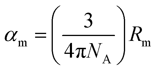


 induces a non-harmonic displacement of the charge carriers (electrons) within a compound (composed of nanoparticles). The induced electric dipole moments, which oscillate at the same frequency as the applied electric field, sum up, leading to the generation of macroscopic polarisation in the irradiated material. In fact, while smaller expansion coefficients render higher-order nonlinearities of little interest in some cases, they can still be significant when resonantly enhanced in matter.87 The macroscopic polarizability can therefore be expressed in terms of the electric field strength according to the following formula:88


