DOI:
10.1039/D5NA00839E
(Paper)
Nanoscale Adv., 2026,
8, 635-645
Inverse design optimization of MIS nanorod arrays to enhance wavelength-selective light extraction of OLEDs through guided SPCE
Received
31st August 2025
, Accepted 16th November 2025
First published on 20th November 2025
Abstract
One of the primary causes of low light extraction efficiency (LEE) in conventional OLEDs is the trapping of light within the substrate layer. To overcome this limitation, various nanostructures have recently been investigated for integration into different OLED layers, aiming to convert the trapped loss modes into out-coupled light and thereby improve LEE. In this work, we propose a simple yet innovative nanorod array design composed of metal, insulator, and semiconductor-oxide layers, integrated on the bottom surface of the OLED structure. This configuration enhances light extraction through guided surface plasmon-coupled emission (SPCE). Using an inverse design-based optimization approach, the structural parameters of the nanorods were optimized to achieve wavelength-selective LEE enhancement. The periodic MIS nanorod array was optimized via the Particle Swarm Optimization (PSO) algorithm for different emission wavelengths, yielding improvements of 29%, 30%, and 51% at 440 nm, 550 nm, and 640 nm, respectively, compared with conventional OLEDs. In addition, the optimized arrays demonstrate high spectral luminous efficiency (SLE), reduced UV transmittance, and uniform emission directionality. These enhancements have significant potential to advance OLED-based display technologies.
Introduction
Organic Light-Emitting Diodes (OLEDs) are thriving in the field of display technologies due to their capability of producing natural colors, low power consumption, fast response, and many other advantages. For high-efficiency light emission, an electron transport layer (ETL), a hole transport layer (HTL), and electron and hole blocking layers have been introduced to enhance the exciton recombination rate in the emission layer. Variation in thickness of the layers, such as the ETL and HTL, has been studied for enhancing LEE of OLEDs.1,2 Micro-patterned low-index grids to extract waveguide modes, anti-reflection layers to reduce total internal reflection (TIR), and deposition of external hierarchical texture on bottom-emitting OLEDs to improve external quantum efficiency (EQE) have been common in OLED structures.3–5 Despite these modifications, progress in OLED performance has stagnated, which demands the emergence of nanostructures in these devices. There are several types of nanostructures integrated into OLEDs, such as periodic nanostructures, randomly distributed nanostructures, metamaterial incorporated OLEDs, bioinspired nanostructures, etc.6–10 Out-coupled efficiency (OCE) of OLEDs represents the ratio of the number of photons extracted outside to the number of recombinations of electrons and holes. In conventional OLEDs, this efficiency is nearly 20%.11 Since EQE of an OLED is the product of its internal quantum efficiency (IQE) and OCE, enhancing the OCE is essential for improving overall device performance. According to Snell's law, approximately 24% of the trapped optical modes in bottom-emitting OLEDs result from total internal reflection (TIR) at the interface between the glass substrate and air, caused by their refractive index mismatch.12 Random nanoparticle-based composite films can be used as an out-coupling layer for flexible OLEDs.13,14 Incorporating periodic nanostructures, for example, 2D photonic crystals of SiO2/SiNx incorporated in a glass substrate using Bragg scattering showed significant improvement of up to 50% in OCE compared to conventional OLEDs.15 A UV-curable acrylate and sol–gel process, combined with planarized ZnO layers, was used to fabricate a photonic crystal substrate of OLEDs, resulting in a notable 38% increase in the OCE.16 Sung et al. fabricated conical SiO2 on the substrate of an OLED. After planarization with TiO2 nanoparticles, 25% improvement in OCE was observed.17 In addition to photonic crystals, a 2D nanomesh was employed in OLEDs to increase extraction efficiency.18 Moreover, inverse design-based optimization techniques have been used in different photonic devices and applications, such as the design of mode converters, optical switches, photonic crystals, etc.19,20
Here, we report the particle swarm optimization (PSO) based inverse design technique for nanostructures to be incorporated on the OLED surface. These periodic nanorods have three layers of metal–insulator–semiconductor oxide (MIS), which significantly improves the LEE of bottom-emitting OLEDs through guided surface plasmon coupled emission (SPCE). A major advantage is that LEE enhancement can be wavelength-selective by changing the structural parameters of the nanorod. The semiconductor-oxide layer will reduce TIR by directing optical modes to the metal–insulator interface of the nanorod, which will increase SPCE from the OLED. This approach aims to offer a new strategy for achieving higher optical outcoupling in bottom-emitting OLED devices along with improved emission intensity, spectral luminous efficiency (SLE), UV light suppression, and uniform directionality.
Loss mechanisms in OLEDs and guided SPCE theory
In OLEDs, EQE is achieved by the multiplication of IQE and OCE, ηEQE = ηIQE × ηOCE. The OCE decreases due to the reflection loss in the glass substrate, known as substrate-guided loss. For a commercially available OLED structure like the one shown in Fig. 1(a), this loss contributes to almost 20% loss of light inside the OLED structure. Only 20% of the light is outcoupled to air according to Fig. 1(b). When light is extracted from a glass substrate to air, it faces reflection due to the refractive index mismatch between glass (RI = 1.45) and air (RI = 1). According to Snell's law, if the light incident angle becomes greater than the critical angle of the interface of two media, it faces TIR loss inside the glass medium. That's why a nanorod-shaped waveguiding medium like ZnO (semiconductor oxide) with a higher refractive index can be integrated at the surface of the glass substrate to support an increased number of optical modes inside the waveguide. The plasmonic nanorod structure, which consists of a metal–dielectric interface on top of the ZnO layer, can emit the guided optical modes through the creation of a surface plasmon, and eventually increase the OLED's light extraction.21
 |
| | Fig. 1 (a) A commercially available OLED structure with different layers. (b) Different types of loss contributions inside a conventional OLED. Only 20% of the light becomes out-coupled to air. | |
In Fig. 2, we have a MIS nanorod array of diameter ‘D’, ZnO thickness ‘L’, and periodicity ‘P’. ‘k’ represents the wavevector of the mode propagating inside the waveguide. The orthogonal components ‘β’ and ‘kx’ are related to the wavevector through the incident angle ‘θ’, which represents their corresponding mode number. Here, kx = k![[thin space (1/6-em)]](https://www.rsc.org/images/entities/char_2009.gif) cosθ and β = ksinθ. Since this is a finite cylindrical waveguide, the mode trapped inside the waveguide will depend on both axial and transverse boundary conditions.22,23 The transverse and axial resonance condition for the cylindrical waveguide is,
cosθ and β = ksinθ. Since this is a finite cylindrical waveguide, the mode trapped inside the waveguide will depend on both axial and transverse boundary conditions.22,23 The transverse and axial resonance condition for the cylindrical waveguide is,
| |  | (1) |
 |
| | Fig. 2 MIS nanorod array placed on a glass substrate. Their structural parameters – ZnO thickness (L), nanorod diameter (D), and periodicity of the array (P) affect the light propagation constants and optical modes inside the nanorod. | |
Now, from Fig. 2, it can be written that
| |  | (2) |
Here,
Pnm refers to the
m – th root of the Bessel function of order
n, which arises from solving the wave equation in cylindrical coordinates with boundary conditions.
l is the mode number which can be
l = 0, 1, 2, 3, … for TM modes and
l = 1, 2, 3, … for TE modes. According to
eqn (2), if the length of the waveguide and the number of modes are fixed, to keep the propagation constant
β real, with increasing wavelength, the peak value of the diameter has to increase. Again, with a fixed wavelength, there is a trade-off between the number of supported modes in the waveguide and the absorption area of the nanorod in the case of a larger diameter. Now, with a fixed diameter, a longer waveguide will be able to support a larger number of modes at a specific wavelength. Experimental results also verify this relation between longer ZnO nanorods and light extraction.
24 Furthermore, dipolar coupling for plasmonic resonance exhibits a red shift with a smaller lattice constant; the peak periodicity for light extraction decreases with increasing wavelength.
21
So, some important performance parameters of OLEDs, such as the radiative decay rate, LEE, angular radiation pattern, color temperature, SLE, and UV light suppression, are affected by the structural parameters of the nanorod array. In this study, we will measure LEE enhancement from the ratio of the farfield transmittance of the MIS nanorod-patterned OLED and the no-patterned OLED structure. Another performance parameter, SLE, can also be measured by using the optical power achieved normalized to human eye sensitivity.
Design principle
Device architecture
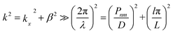
An OLED is an injection-type device comprising two electrodes separated by an organic multilayer. The thickness of different layers and the energy band diagram of our studied OLED device are illustrated in Fig. 3(a) and (b). The used OLED device employs Al as the cathode, Alq3 as the electron transport layer (ETL), α-NPD as the hole transport layer (HTL), ITO as the anode, SiN as the encapsulation layer, and glass as the substrate. For evaluating LEE enhancement, identical OLED structures were simulated with and without an MIS nanorod array on the substrate. A single MIS nanorod structure and the growth process of the nanorods are illustrated in Fig. 3(c) and (d).
 |
| | Fig. 3 (a) Thickness of different layers in OLEDs with MIS nanorods placed on the surface of the glass substrate which enhances light extraction through SPCE. (b) Energy band diagram of the OLED device. (c) A single nanorod structure made of ZnO, dielectric, and metal (Ag/Au/Cu) layers. (d) Growth process of the MIS nanorod array on the substrate layer. Controlled growth of ZnO nanorods will be followed by dielectric coating. Finally, the metal layer will be deposited. | |
ZnO was selected as the semiconductor oxide, while the dielectric and metal thickness and dielectric material were determined from broadband transmittance across the visible range by changing those parameter values.
Optimization algorithm
The structural parameters of the nanorod array (ZnO thickness, nanorod radius, and periodicity) have been optimized using the inverse-design optimization technique at three distinct wavelengths of 440 nm, 550 nm, and 640 nm for blue, green, and red emitting OLEDs. To observe the trend of LEE enhancement compared to conventional OLEDs for varying a single parameter, every parameter is varied in a specific range. Then the boundary values for these parameters are set for the optimization algorithm, which is known as the Particle Swarm Optimization (PSO) algorithm. The algorithm flow chart to achieve the optimum parameter values is depicted in Fig. 4. The algorithm consists of one judgmental unit (optimum) and two processing units (PSO and FDTD). In the PSO unit, every particle will find its personal best parameters and compare them with the global parameters. Then the cognitive and social components will be added to the current velocity of the particles, which is multiplied by the inertia weight w. Thus, the algorithm will adjust the new position of the particles (new structural parameters).| | | vi (t + 1) = wvi(t) + c1r1(pBesti − xi) + c2r2(gBesti − xi) xi(t +1) = xi(t) + vi(t + 1) | (3) |
Here, r1 and r2 are random matrices regenerated after every iteration and bounded in the [0, 1] range, and c1 and c2 are coefficients for cognitive and social components. Based on the requirement of increasing LEE, the near-field transmission of light, Tnear-field, which is the figure of merit in the optimization algorithm, is monitored by using a field monitor placed above the OLED structure, completing forward simulations in FDTD. The figure of merit is defined as follows:| | | maximize f(L,D,P) = |Tnear-field| | (4) |
 |
| | Fig. 4 The algorithm flow chart of inverse design optimization of OLEDs with MIS nanorods, which provides optimal parameter values of the structure. | |
The Finite Difference Time Domain (FDTD) method was employed to solve Vector 3D Maxwell's equations for forward simulations with the parameter values obtained from optimization. The Perfectly Matched Layers (PML) boundary conditions were applied to reduce the computational load and avoid the unnecessary reflection of light at the computational boundaries, and metal boundary conditions were used in the cathode layer. Multiple dipole sources were positioned using unit cell symmetry to simulate the behaviour of light inside the OLED structure.25 Different locations and orientations of dipole sources have been implemented through parameter sweep. A frequency domain field profile monitor captured the data of time domain electric and magnetic fields and the transmitted power near the structure. Then the time-domain field was converted to the frequency domain using the Fourier transform. These frequency domain fields are projected into the far-field through directional vectors accounting for Snell's law and Fresnel's law of reflection occurring at the far-field interface.
Results and analysis
Guided SPCE
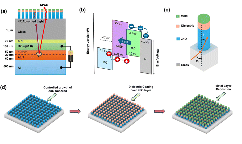
The effect of metal layer thickness in the nanorod on SPP generation was first investigated, given its direct impact on light absorption. In addition, variations in the dielectric refractive index and thickness were explored to find the optimum plasmonic structure. From Fig. 5(a), it is seen that 10 nm metal thickness results in maximum light transmission in the visible range.A steady increase in light transmittance is observed at a dielectric thickness of 30 nm in Fig. 5(b), and the change in refractive index of the dielectric material shows a minimal variation in light transmission as shown in Fig. 5(c). From the observations, a metal layer thickness of 10 nm, Al203, RI = 1.7–1.8 in the visible range, as the dielectric layer, and a dielectric thickness of 30 nm have been used as the plasmonic section of the structure for the optimization process.
 |
| | Fig. 5 Transmission spectra of the MIS nanorod structure under varying meta-dielectric design parameters: (a) metal layer thickness (10 nm, 20 nm, and 30 nm); (b) dielectric layer thickness (30 nm, 60 nm, and 90 nm); and (c) refractive index of the dielectric layer (RI = 1.8, 2.0, 2.3). | |
To choose the metal, enhancement of light intensity at the metal–dielectric interface for different metals (Au, Cu, and Ag) is observed in Fig. 6(a–c), which confirms SPP generation from guided light waves. Ag exhibits strong surface plasmon confinement in the wavelength range of 400–450 nm, while Au demonstrates maximum confinement near 530 nm and Cu at around 600 nm. That's why Ag, Au, and Cu can be used for blue, green, and red emission regions, respectively, due to their distinct plasmonic responses at the corresponding wavelengths.21 ZnO nanorods as a resonator-type waveguide scatter the field to localized light.26,27 This resonance induced a stronger electric field along the nanorod gaps due to the refractive index contrast between ZnO and air, causing light refraction at the nanorod–air interface as per Snell's law.28,29
 |
| | Fig. 6 Generation of SPPS at the metal–dielectric interface of the nanorod for different metals from guided light in the ZnO layer: (a) for Ag at 440 nm, (b) for Au at 550 nm, and (c) for Cu at 640 nm. | |
LEE enhancement trend
After defining the plasmonic structure, the enhancement trend of light extraction efficiency (LEE) at 440, 550, and 640 nm was investigated by systematically varying the structural parameters of the MIS nanorods, including ZnO thickness (L), nanorod radius (R), and array periodicity (P).
As shown in Fig. 7(a), the LEE enhancement curve increases with ZnO thickness for the three wavelengths. As shown in Fig. 7(b), the optimal nanorod radius shifts to larger values with increasing wavelength (red shift). However, at a fixed wavelength, the peak radius decreases beyond a critical point because of the larger absorption area for the photon. Finally, Fig. 7(c) demonstrates that the peak periodicity shifts to a smaller value as the wavelength faces a red shift. LEE enhancement maximizes at 440 nm, 550 nm, and 640 nm wavelengths for the corresponding usage of Ag, Au, and Cu as metal layers, as expected, which is portrayed in Fig. 7(d). The enhancement trends for different structural parameters with respect to wavelength shifting follow the theoretical estimation depicted in the previous section with eqn (2).
 |
| | Fig. 7 LEE enhancement trends at 440 nm, 550 nm, and 640 nm emission wavelengths for different structure parameters: (a) ZnO thickness; (b) nanorod radius; (c) periodicity of the array; (d) metal types as the top layer. | |
Although various metals exhibit distinct plasmon resonance frequencies and can enhance light intensity at their respective emission wavelengths, integrating multiple metal layers within a single OLED unit for display applications is impractical from a fabrication standpoint. From Fig. 8, it can be observed that Au and Cu enhance light extraction consistently across the visible spectrum. In contrast, Ag exhibits stronger enhancement in the blue emission region but tends to absorb more light at longer (red) wavelengths, rather than efficiently exciting SPPs. Therefore, Au or Cu emerges as the more practical choice for the proposed design.
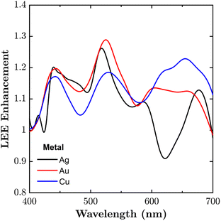 |
| | Fig. 8 Au and Cu exhibit broadband enhancement across the visible range (400 nm–700 nm), while Ag shows a pronounced peak in the blue emission region but reduced performance in the red region due to higher absorption losses. | |
Optimization results
Observing the parameter trends, the boundary values set for the PSO algorithm are ZnO thickness [100 nm–800 nm], nanorod radius [30 nm –80 nm], and array periodicity [180 nm–350 nm]. After 25 iterations, the objective function reaches a converged value and provides optimized structure parameters for all three wavelengths, as shown in Fig. 9. Since multiple parameters affect the transmittance, there can be more than one optimized combination to achieve the optimal figure of merit. The combinations of optimized parameters to achieve the maximum objective function are listed in Table 1. If we look at the optimized parameters, for example, at 440 nm wavelength, ZnO thickness has reduced while the nanorod radius has increased in the 2nd combination compared to the 1st one. This trend has also been followed for the combinations at 550 and 640 nm wavelengths. So, the optimized parameter values reconfirm eqn (2) that for resonance at a particular wavelength, if one parameter between L and D reaches the maximum value, the other one will try to reach the minimum to incorporate maximum optical mode. By reducing the nanorod length and increasing its radius, the proposed structure can enhance light extraction, decreasing the vertical footprint of the device relative to previously reported results at the same time.30 Although our algorithm explored different metals to optimize performance across various emission regions, Au or Cu should ultimately be selected for manufacturing owing to their ability to enhance light extraction effectively across the entire visible wavelength range, as discussed in the preceding subsection.
 |
| | Fig. 9 Updated value of near-field transmittance after each iteration from the PSO algorithm at (a) 440 nm; (b) 550 nm; (c) 640 nm wavelength. | |
Table 1 Optimized structural parameters of MIS nanorod arrays for different metals
| Wavelength |
ZnO thickness (nm) |
Nanorod radius (nm) |
Array periodicity (nm) |
Metal |
Max transmittance |
LEE enhancement (%) |
|
λ = 440 nm |
150.31 |
74.00 |
250.00 |
Ag |
0.2066 |
29.12 |
| 100.00 |
80.00 |
350.00 |
|
|
|
|
λ = 550 nm |
105.67 |
78.89 |
204.06 |
Au |
0.1447 |
30.36 |
| 100.00 |
80.00 |
180.00 |
|
|
|
|
λ = 640 nm |
136.48 |
68.30 |
195.03 |
Cu |
0.1442 |
51.78 |
| 120.26 |
74.97 |
185.75 |
|
|
|
With the optimized MIS nanorod structure on the OLED surface, other key performance parameters, including emission intensity, color temperature, far-field angular distribution, SLE, transmittance at UV wavelength, and electrical characteristics, were also analyzed.
Optical performance
As shown in Fig. 10(a–c), the optimized MIS nanorods enhance emission intensity across the blue, green, and red spectral regions. The maximum emission intensity increases for red OLEDs by almost 2 times. It also increases by 1.33 times and 1.42 times for green and blue OLEDs, respectively. The linewidth of the spectrum has become broader for all the OLEDs.
 |
| | Fig. 10 Enhanced emission intensity after incorporating MIS nanorods on the glass surface for (a) blue, (b) green and (c) red emitting OLED devices. MIS nanorods on the glass surface for (a) blue, (b) green and (c) red emitting OLED devices. Comparative analysis of angular radiation patterns between a conventional OLED and MIS nanorod integrated OLED at (d) λ = 440 nm, (e) λ = 550 nm, and (f) λ = 640 nm wavelengths. | |
Subsequently, the angular radiation intensity was analyzed for the simulated OLED without a nanorod array and with the optimized nanorod array on the substrate surface. The angular coverage of the light intensity of these two devices at wavelengths of 440 nm, 550 nm, and 640 nm is portrayed in Fig. 10(d–f). At λ = 440 nm and λ = 640 nm, the radiation pattern remains nearly unchanged, whereas at λ = 550 nm the incorporation of MIS nanorods leads to a more uniform light intensity distribution. The effective viewing angle for the proposed device expands up to 30°.
Another performance parameter, the spectral luminosity efficiency (SLE), was measured at 440, 550, and 640 nm wavelengths for the optimized MIS nanorod structures incorporated on the OLED surface, as demonstrated in Fig. 11(a). The SLE values obtained at emission wavelengths of 440 nm, 550 nm, and 640 nm are 5.07%, 62.57%, and 45.57%, respectively. The highest SLE is obtained at a wavelength of 550 nm, which corresponds to the maximum overlap with the human eye's luminosity function. In contrast, the blue emission at 440 nm exhibits the lowest SLE, primarily due to fluorescence-related limitations.31
 |
| | Fig. 11 (a) SLE values at 440 nm, 550 nm, and 640 nm emission wavelengths for optimized MIS nanorod structures incorporated on the OLED surface. (b) UV transmittance reduces at 250 nm, 300 nm, 350 nm, and 400 nm wavelengths by using MIS nanorods, which were optimized for blue (440 nm), green (550 nm), and red (640 nm) emission, compared to the conventional OLED structure without nanorods. | |
Another advantage of incorporating optimized nanorods on the glass surface is the effective suppression of UV wavelengths. The optimized parameters corresponding to emission wavelengths of 440 nm, 550 nm, and 640 nm significantly decrease the UV light output from OLEDs compared to conventional structures. The transmittance in this region reduces from 12% to 5–7% because of the nanorod structure on top. In particular, the optimized MIS nanorod design for 550 nm emission reduces the transmittance to below 5% in the deep UV region, representing a comparable improvement with the state of the art.32 The reduction of UV light at 250 nm, 300 nm, 350 nm, and 400 nm wavelengths achieved by introducing optimized nanorods for blue, green, and red emission on the OLED surface is presented in a grouped bar chart in Fig. 11(b).
Electrical performance
We have also compared the electrical characteristics and found no change in internal quantum efficiency (IQE) and J–V plots between a conventional OLED and OLED with MIS nanorods, as shown in Fig. 12. Since the MIS nanorod array on the glass surface is a light extraction structure, it will not have any impact on the photon generation from electron–hole pair recombination in the emitting layer, and the photon recycling effect is also not considered. From the inset of the graphs, the maximum IQE for our studied OLED structure is 12.5% and the cutoff voltage is found to be 1.8 V.
 |
| | Fig. 12 Comparative analysis of (a) IQE; (b) J–V characteristics between OLEDs with and without MIS nanorods. The voltage at which IQE becomes saturated and the cut-off voltage are portrayed in the inset of the graphs. | |
Fabrication and experimental validation
For the growth of ZnO nanostructures, various techniques are used, including pulsed laser deposition,33,34 chemical vapor deposition,35 electrochemical deposition,36 hydrothermal,37 atomic layer deposition38 and chemical bath deposition.39 Compared with many of the previously mentioned techniques, chemical bath deposition (CBD) is a relatively low-temperature and low-cost ZnO synthesis method based on a relatively simple procedure. Deposition of metal and dielectric layers can also be achieved through methods like e-beam evaporation and sputtering.40 Numerous studies have reported the growth of ZnO nanorod arrays on LED substrates to improve light extraction efficiency.25,30,41,42 These experimental findings corroborate our simulation results, demonstrating the dependence of LEE on both the ZnO nanorod length30,41 and the array periodicity.42 Furthermore, the electric field measurements presented in these studies validate our simulated enhancement of light intensity attributed to plasmonic effects, as obtained using the Ansys Lumerical FDTD solver. The optimization of structural parameters through the inverse design algorithm further reinforces the validity of our proposed structure, as the simulated and experimental outcomes show strong agreement with theoretical predictions.
Conclusion
Integration of optimized periodic MIS nanorod arrays on the substrate surface of the OLED substrate has led to a significant enhancement in LEE through the guided surface plasmon-coupled emission. These findings not only address the total internal reflection losses in the substrate layer of OLEDs but also demonstrate the process for wavelength-selective emission tuning. The LEE enhancement achieved at 440, 550, and 640 nm with increased emission intensity suggests promising applications in high-performance displays and energy-efficient lighting. This inverse design optimization technique can contribute to the future development of nanostructured optoelectronic devices. Future research may explore alternative materials and scalable fabrication for further performance and cost optimization.
Author contributions
Khondokar Zahin: conceptualization, data curation, formal analysis, investigation, methodology, software, validation, visualization, writing – original draft. A. K. M Hasibul Haque: formal analysis, methodology, writing – review & editing. Md. Jawadul Karim: software, writing – review & editing. Ying Yin Tsui: resources, validation, writing – review & editing. Md Zahurul Islam: supervision, project administration, resources, investigation, conceptualization, methodology, funding acquisition, formal analysis, validation, writing – review & editing.
Conflicts of interest
The authors declare no conflicts of interest.
Data availability
Data for this article, including LEE enhancement and optimization data are available at http://https://github.com/kh−zahin/MIS−Nanorod−OLED−LEE.git.
Acknowledgements
The authors acknowledge the financial grant (Basic Research Grant, BUET, Office Order no.: Shongstha/R-60/Re-2413, Dated: 10 Oct 2023, DMZI) and logistical support provided by the Department of EEE, BUET throughout the duration of this work.
References
- B.-Y. Lin, Y.-R. Li, C.-H. Chen, H.-C. Hsu, M.-K. Wei, J.-H. Lee and T.-L. Chiu, Effects of electron transport layer thickness on light extraction in corrugated OLEDs, Opt. Express, 2022, 30, 18066–18078 CrossRef CAS PubMed.
- H. Ulla, M. R. Kiran, S. N. Ansari, M. W. Alam, W. M. Girma and G. Gedda, Effect of hole-transport layer thickness on the performance of organic light-emitting diodes, Opt. Mater., 2024, 147, 114602 CrossRef CAS.
- S. Chen, J. Xie, Y. Yang, C. Chen and W. Huang, High-contrast top-emitting organic light-emitting diodes with a Ni/ZnS/CuPc/Ni contrast-enhancing stack and a ZnS anti-reflection layer, J. Phys. D: Appl. Phys., 2010, 43, 365101 CrossRef.
- Y. Sun and S. R. Forrest, Enhanced light out-coupling of organic light-emitting devices using embedded low-index grids, Nat. Photonics, 2008, 2, 483–487 CrossRef CAS.
- M. Kovačič, D. Samigullina, F. Bouchard, J. Krč, B. Lipovšek, M. Soldera, A. F. Lasagni, S. Reineke and M. Topič, Analysis and optimization of light outcoupling in OLEDs with external hierarchical textures, Opt. Express, 2021, 29, 23701–23716 CrossRef PubMed.
- Y. Zhang, R. Biswas, R. Shinar and J. Shinar, Simulation of enhanced light extraction from periodic, disordered, and quasi-periodic OLED structures, J. Opt. Soc. Am. B, 2021, 38, C144–C152 CrossRef.
- Y. D. Kim, K.-H. Han, Y. H. Sung, J.-B. Kim, H.-J. Choi, H. Lee and J.-J. Kim, Enhanced light extraction efficiency in organic light-emitting diode with randomly dispersed nanopattern, Opt. Lett., 2015, 40, 5838–5841 CrossRef CAS PubMed.
- W. Zhu, T. Xiao, G. Zhai, J. Yu, G. Shi, G. Chen and B. Wei, A facile method to enhance out-coupling efficiency in organic light-emitting diodes via a random-pyramids textured layer, J. Phys. D: Appl. Phys., 2016, 49, 385103 CrossRef.
- K. Kang, S. Im, C. Lee, J. Kim and D. Kim, Nanoslot metasurface design and characterization for enhanced organic light-emitting diodes, Sci. Rep., 2021, 11, 9232 CrossRef CAS PubMed.
- J.-J. Kim, Y. Lee, H. G. Kim, K.-J. Choi, H.-S. Kweon, S. Park and K.-H. Jeong, Biologically inspired LED lens from cuticular nanostructures of firefly lantern, Proc. Natl. Acad. Sci. U. S. A., 2012, 109, 18674–18678 CrossRef CAS PubMed.
- N. C. Greenham, R. H. Friend and D. D. Bradley, Angular dependence of the emission from a conjugated polymer light-emitting diode: implications for efficiency calculations, Adv. Mater., 1994, 6, 491–494 CrossRef CAS.
- Y.-J. Lee, S.-H. Kim, J. Huh, G.-H. Kim, Y.-H. Lee, S.-H. Cho, Y.-C. Kim and Y. R. Do, A high-extraction-efficiency nanopatterned organic light-emitting diode, Appl. Phys. Lett., 2003, 82, 3779–3781 CrossRef CAS.
- C.-H. Shin, G. Huseynova, E. Kim, J. Lee, S. Yoo, Y. Choi and J.-H. Lee, Random Al2O3 nanoparticle-based polymer composite films as outcoupling layers for flexible organic light-emitting diodes, Opt. Express, 2020, 28, 26170–26179 CrossRef CAS PubMed.
- Y. Gu, D.-D. Zhang, Q.-D. Ou, Y.-H. Deng, J.-J. Zhu, L. Cheng, Z. Liu, S.-T. Lee, Y.-Q. Li and J.-X. Tang, Light extraction enhancement in organic light-emitting diodes based on localized surface plasmon and light scattering double-effect, J. Mater. Chem. C, 2013, 1, 4319–4326 RSC.
- Y. R. Do, Y.-C. Kim, Y.-W. Song and Y.-H. Lee, Enhanced light extraction efficiency from organic light emitting diodes by insertion of a two-dimensional photonic crystal structure, J. Appl.
Phys., 2004, 96, 7629–7636 CrossRef CAS.
- H.-H. Cho, B. Park, H.-J. Kim, S. Jeon, J.-h. Jeong and J.-J. Kim, Solution-processed photonic crystals to enhance the light outcoupling efficiency of organic light-emitting diodes, Appl. Opt., 2010, 49, 4024–4028 CrossRef CAS PubMed.
- Y. H. Sung, P.-H. Jung, K.-H. Han, Y. D. Kim, J.-J. Kim and H. Lee, Improved out-coupling efficiency of organic light emitting diodes fabricated on a TiO2 planarization layer with embedded Si oxide nanostructures, Opt. Mater., 2017, 72, 828–832 CrossRef CAS.
- W. Ding, Y. Wang, H. Chen and S. Y. Chou, Plasmonic nanocavity organic light-emitting diode with significantly enhanced light extraction, contrast, viewing angle, brightness, and low-glare, Adv. Funct. Mater., 2014, 24, 6329–6339 CrossRef CAS.
- M. Wei, X. Lin, K. Xu, Y. Wu, C. Wang, Z. Wang, K. Lei, K. Bao, J. Li and L. Li, others Inverse design of compact nonvolatile reconfigurable silicon photonic devices with phase-change materials, Nanophotonics, 2024, 13, 2183–2192 CrossRef CAS PubMed.
- M. Minkov, I. A. Williamson, L. C. Andreani, D. Gerace, B. Lou, A. Y. Song, T. W. Hughes and S. Fan, Inverse design of photonic crystals through automatic differentiation, ACS Photonics, 2020, 7, 1729–1741 CrossRef CAS.
-
S. A. Maier,Plasmonics: Fundamentals and Applications, Springer, 2007, vol. 1 Search PubMed.
-
M. Benson, Fields, Waves and Transmission Lines, Springer Science & Business Media, 2012 Search PubMed.
-
S. Y. Liao, Microwave Devices and Circuits, Pearson Education India, 1990 Search PubMed.
- H. Jeong, R. Salas-Montiel and M. S. Jeong, Optimal length of ZnO nanorods for improving the light-extraction efficiency of blue InGaN light-emitting diodes, Opt. Express, 2015, 23, 23195–23207 CrossRef CAS PubMed.
- J. Lu, Z. Shi, Y. Wang, Y. Lin, Q. Zhu, Z. Tian, J. Dai, S. Wang and C. Xu, Plasmon-enhanced electrically light-emitting from ZnO nanorod arrays/p-GaN heterostructure devices, Sci. Rep., 2016, 6, 25645 CrossRef CAS PubMed.
- G. M. Mangalgiri, P. Manley, W. Riedel and M. Schmid, Dielectric nanorod scattering and its influence on material interfaces, Sci. Rep., 2017, 7, 4311 CrossRef PubMed.
- J. Van de Groep and A. Polman, Designing dielectric resonators on substrates: combining magnetic and electric resonances, Opt. Express, 2013, 21, 26285–26302 CrossRef CAS PubMed.
- Y.-H. Hsiao, C.-Y. Chen, L.-C. Huang, G.-J. Lin, D.-H. Lien, J.-J. Huang and J.-H. He, Light Extraction Enhancement with Radiation Pattern Shaping of LEDs by Waveguiding Nanorods with Impedance-Matching Tips, Nanoscale, 2014, 6, 2624–2628 RSC.
- J. Y. Kim and F. E. Osterloh, ZnO–CdSe Nanoparticle Clusters as Directional Photoemitters with Tunable Wavelength, J. Am. Chem. Soc., 2005, 127, 10152–10153 CrossRef CAS PubMed.
- O. H. Kwon, J. W. Jang, S.-J. Park, J. S. Kim, S. J. Hong, Y. S. Jung, H. Yang, Y. J. Kim and Y. S. Cho, Plasmonic-enhanced luminescence characteristics of microscale phosphor layers on a ZnO nanorod-arrayed glass substrate, ACS Appl. Mater. Interfaces, 2018, 11, 1004–1012 CrossRef.
- I. Siddiqui, S. Kumar, Y.-F. Tsai, P. Gautam, Shahnawaz, K. Kesavan, J.-T. Lin, L. Khai, K.-H. Chou, A. Choudhury, S. Grigalevicius and J.-H. Jou, Status and Challenges of Blue OLEDs: A Review, Nanomaterials, 2023, 13, 2521 CrossRef CAS.
- L. Chen, H. Gu, X. Guo, M. Xu, T. Shi, J. Li, W. Cao and S. Liu, Simultaneously improving color purity, stability, and health-friendliness of OLEDs via optimally designed color filters, Opt. Express, 2025, 33, 13506–13518 CrossRef.
- Y. Sun and Y. Tsui, Production of porous nanostructured zinc oxide thin films by pulsed laser deposition, Opt. Mater., 2007, 29, 1111–1114 CrossRef CAS.
- M. Taschuk, Y. Sun and Y. Tsui, Angularly resolved photoluminescent emission from pulsed-laser-deposited ZnO films with different microstructures, Appl. Phys. A:Mater. Sci. Process., 2008, 90, 141–147 CrossRef CAS.
- T. M. K. Thandavan, S. M. A. Gani, C. San Wong and R. Md. Nor, Enhanced photoluminescence and Raman properties of Al-doped ZnO nanostructures prepared using thermal chemical vapor deposition of methanol assisted with heated brass, PLoS One, 2015, 10, e0121756 CrossRef PubMed.
- S. Sun, S. Jiao, K. Zhang, D. Wang, H. Li, S. Gao, J. Wang, Q. Yu, F. Guo, L. Zhao and others, Morphology and properties of ZnO nanostructures by electrochemical deposition: effect of the substrate treatment, J. Mater. Sci.: Mater. Electron., 2013, 24, 85–88 CrossRef CAS.
- Z. Dong, B. Han, S. Qian and D. Chen, Fluorescent properties of ZnO nanostructures fabricated by hydrothermal method, J. Nanomater., 2012, 2012, 251276 CrossRef.
- K. R. Nandanapalli and D. Mudusu, Surface passivated zinc oxide (ZnO) nanorods by atomic layer deposition of ultrathin ZnO layers for energy device applications, ACS Appl. Nano Mater., 2018, 1, 4083–4091 CrossRef CAS.
- K. O. Zheng, N. Rosli, M. Rashid and M. M. Halim, Electrically pumped random laser device based on Pd/SiO2/ZnO nanorods MIS structure, Results Phys., 2024, 64, 107946 CrossRef.
- L. P. Hackett, A. Ameen, W. Li, F. K. Dar, L. L. Goddard and G. L. Liu, Spectrometer-free plasmonic biosensing with metal–insulator–metal nanocup arrays, ACS Sens., 2018, 3, 290–298 CrossRef CAS PubMed.
- H. Jeong, R. Salas-Montiel and M. S. Jeong, Optimal length of ZnO nanorods for improving the light-extraction efficiency of blue InGaN light-emitting diodes, Opt. Express, 2015, 23, 23195–23207 CrossRef CAS PubMed.
- K.-K. Kim, S.-d. Lee, H. Kim, J.-C. Park, S.-N. Lee, Y. Park, S.-J. Park and S.-W. Kim, Enhanced light extraction efficiency of GaN-based light-emitting diodes with ZnO nanorod arrays grown using aqueous solution, Appl. Phys. Lett., 2009, 94, 071118 CrossRef.
|
| This journal is © The Royal Society of Chemistry 2026 |
Click here to see how this site uses Cookies. View our privacy policy here. 
 Open Access Article
 This Open Access Article is licensed under a Creative Commons Attribution-Non Commercial 3.0 Unported Licence
 *a
*a


