
 Open Access Article
 This Open Access Article is licensed under a Creative Commons Attribution-Non Commercial 3.0 Unported Licence
Lead-free metal halide layered double perovskites as sustainable platforms: composition tuning, synthetic methods and advanced applications
Kavitha H.
 a,
Sangita Das
b and
Partha Pratim Das
*a
a,
Sangita Das
b and
Partha Pratim Das
*a
aManipal Institute of Technology, Manipal Academy of Higher Education, Manipal-576104, Karnataka, India. E-mail: partha.das@manipal.edu
bDepartment of Biochemistry, School of Chemical Sciences, St Joseph's University, Bengaluru-560027, Karnataka, India
First published on 22nd May 2026
Abstract
The growing demand for environmentally friendly and stable materials has accelerated research into lead-free alternatives for optoelectronic and energy applications. Among these, layered double perovskites (LDPs) with the general formula A4B(II)B(III)2X12 have gained attention due to their structural versatility, tunable optoelectronic properties and enhanced stability. This review critically examines compositional engineering in mixed-metal halide LDPs, focusing on how targeted modification of cationic and anionic sublattices governs their optoelectronic behaviour. The molecular source of band gap tunability, photoluminescence properties, defect tolerance, and structural stability are highlighted, providing a unified perspective on structure–property correlations in this material class. The impact of synthetic techniques is further investigated, demonstrating how regulated crystallisation pathways from bulk and single crystals to nanostructures and thin films dictate morphology, defect landscape, and phase purity, ultimately determining material performance. The integration of composition design with synthesis control has been demonstrated to be necessary for unlocking the full potential of LDPs. Recent advances in the applications of tailored LDP compositions in energy conversion and optoelectronic devices are discussed to illustrate their growing technological relevance. Overall, this review aims to provide a unified understanding of the structure–property–function relationship in lead-free LDPs, while also identifying future directions for high-performance, environmentally benign lead-free perovskite-based systems.
 Kavitha H. | Kavitha Hosamane is a PhD student at Manipal Institute of Technology, Manipal Academy of Higher Education (MAHE), Manipal, India. She obtained her master's degree in Organic Chemistry in 2024 from SDM College, Ujire, Karnataka, India. In 2024, she commenced her PhD at MAHE under the supervision of Dr Partha Pratim Das. Her research focuses on lead-free metal halide perovskites for optoelectronic applications. |
 Sangita Das | Dr Sangita Das is an Assistant Professor at St. Joseph's University, Bangalore, India. Her research interests include organic and supramolecular chemistry, fluorescence sensing, molecular recognition, advanced functional materials, and drug delivery systems. She completed her PhD from the Indian Institute of Engineering Science and Technology, Shibpur, India under the CSIR-JRF programme in 2011. She was awarded the prestigious Newton International Fellowship and conducted research at Durham University, UK (2019–2021), followed by research activities at KIST Europe, Germany in 2022. She has published extensively in reputed international journals and edited scientific books in sensing and biomedical materials. |
 Partha Pratim Das | Dr Partha Pratim Das is an Assistant Professor at the Manipal Institute of Technology, Manipal Academy of Higher Education, Manipal, India. He received his PhD in Chemistry from Jadavpur University, Kolkata, India in 2016, with research conducted at CSIR-Central Glass and Ceramic Research Institute, Kolkata and CSIR-National Chemical Laboratory, Pune, India. He subsequently pursued postdoctoral research at Yonsei University and Seoul National University, South Korea under nationally funded research programmes (2016–2022). His research focuses on the processing, structure, and optoelectronic properties of advanced functional materials under varied conditions, with particular emphasis on sustainable energy and environmental applications. |
1. Introduction
1.1 Metal halide perovskites
Recently, metal halide perovskites have turned out to be the most promising class of functional materials for various applications, including photocatalytic CO2 reduction, photovoltaic (PV) cells, light emitting diodes (LEDs), photodetectors, lasers and scintillators owing to their remarkable optical and electronic properties as well as their ease of solution processibility.1–3The basic perovskite structure follows the general formula ABX3, where B is a divalent cation that occupies the BX6 octahedral center and A is a monovalent cation that occupies the interspace of the octahedral BX6 framework coordinated with X anions. The metal halide perovskites show excellent optoelectronic properties such as optical absorption, narrow band gaps, superior charge carrier mobility, photoluminescence, defect tolerance, conductivity, etc.4,5 As reflected by the strong broad absorption in the visible region of the solar spectrum, metal halide perovskites possess outstanding optical absorption property that can be utilized for visible light optoelectronics.6 A notable example is methylammonium lead iodide (MAPbI3), one of the extensively explored perovskite materials in various applications including photovoltaic cells, photodetectors and LEDs owing to its excellent optoelectronic properties.7–9
Despite the rapid increase in the power conversion efficiency of the lead-based perovskites in a short period of time, they face many challenges. The first drawback of lead-based perovskites is the degradation of the compound upon exposure to oxygen and moisture.10 The one more major drawback is its toxicity. The lead metal we get from earth crust is toxic, but the lead halide that is formed as the degradation product of metal halide perovskites is even more toxic than the lead metal.11 Researchers have found several ways of replacing lead to develop non-toxic, stable and highly efficient perovskite materials.
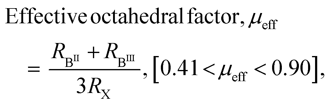
To replace toxic Pb2+ in perovskites, isoelectronic cations such as Sn2+ and Ge2+ have been explored due to their similar outer ns2 electronic configuration. Sn-based perovskites showed narrower optical bandgaps and high carrier mobilities compared to the lead-based perovskites. Nevertheless, the instability of Sn2+ prone to oxidation leads to the formation of vacancies, which promote charge carrier recombination and degrade performance. However, no other divalent cations showed suitable optical activity in replacement of lead.12,13 To synthesize a stable perovskite the ionic radius and charge neutrality conditions must be considered. The octahedral factor (RB/RX) must be within the range of 0.44 to 0.90 and the tolerance factor of the material should be in the range of 0.813 to1.107 to get a stable perovskite structure. The tolerance factor can be calculated by using the formula (RA + RX)/2[RB + RX], where RA, RB and RX are the ionic radii of the A-site cation, B-site cation, and X-site anion respectively.10
In pursuit of environmentally benign and stable alternatives to lead-based perovskites, less toxic trivalent cations such as Bi3+ and Sb3+ have emerged as promising candidates giving rise to the layered structure with the formula A3B2X9. Bismuth-based perovskites, in particular, have demonstrated superior stability compared to their lead-containing counterparts.14 However, their optoelectronic performance remains limited due to intrinsic challenges, including indirect and wide bandgaps, large carrier effective masses, low carrier mobility, and poor defect tolerance.15 Antimony is in the same group as that of bismuth and can be a good replacement of lead as it has outer ns2 configuration as in the case of lead. The zero-dimensional dimer phase of antimony-based compounds suffers from indirect band gaps and low carrier transport.16 The two-dimensional layered phase shows better performance compared to the dimer phase. Nevertheless, the efficiency of antimony-based perovskites remains modest. Recent efforts have focused on band gap engineering particularly through doping strategies to optimize absorption in alignment with the solar spectrum.17 In addition to heterovalent replacement, another promising approach for mitigating the limitations of lead-based perovskites involves the development of double perovskite structures.18,19 In this strategy, two divalent lead ions are replaced either by the vacancy ordered tetravalent metal ions or by the combination of trivalent and monovalent ions, resulting in compounds with general formulas A2B(IV)X6 and A2B(I)B(III)X6 respectively.20–22 There is still scope for the discovery of new materials based on incorporation of different combinations of metals for the betterment of optoelectronic properties.
1.2 Layered double perovskites (LDPs)
LDPs represent an emerging class of lead-free halide perovskites formed by combining heterovalent cation substitution, with dimensional reduction of three-dimensional double perovskite frameworks. This design strategy enhances compositional diversity, structural stability, and tunability of optoelectronic properties. LDPs can be broadly classified based on their crystallographic orientation (e.g., 100 and 111 oriented structures) as well as the nature of the spacer cations.4 In particular, LDPs incorporating organic spacer cations form hybrid structures that are further categorised into Ruddlesden–popper (RP) and Dion–Jacobson (DJ) phases, depending on whether monovalent or divalent organic spacers are present. These organic–inorganic hybrid LDPs offer additional flexibility in tuning interlayer interactions, octahedral distortions and electronic properties.23 In contrast, fully inorganic LDPs typically exhibit improved thermal and environmental stability. Among the various compositions, 111 oriented LDPs with the general formula A4B(II)B(III)2X12 have attracted particular attention due to their structural simplicity, enhanced stability, and promising optoelectronic characteristics.21.3 A4B(II)B(III)2X12 family of materials
The LDPs having the general formula A4B(II)B(III)2X12 have emerged considering the advantages of both layered and double perovskites to give the combined improvement in stability and optoelectronic properties as illustrated in Fig. 1. Here, the A-site typically denotes a monovalent cation, while B(II) and B(III) are divalent and trivalent metal cations, respectively, coordinated by halide ions.2,24 Based on the presence of four A-site cations in their chemical formula, these LDPs are commonly referred to as quadruple perovskites. These compounds form a layered architecture with alternating metal-halide octahedral sheets, differing from the classical 3D perovskites while offering a tunable lattice framework. Such configurations have been explored primarily in compositions like Cs4Cu(II)Sb2(III)Cl12 which is a very first member of this family.25 While lead free strategies address toxicity in halide perovskites, all inorganic heterometallic A4B(II)B(III)2X12 LDPs stand out for their large compositional space, tunable optoelectronic properties, enhanced structural stability and their potential application in various emerging fields. These traits position LDPs as superior alternatives when compared to other lead-free perovskites.26 | ||
| Fig. 1 Schematic showing the emergence of A4B(II)B(III)2X12 metal halide layered double perovskites. | ||
The possibility of forming these quadruple perovskite crystal structures and their phase stability can be predicted by the modified Goldschmidt parameters specific to the A4B(II)B(III)2X12 family of materials; and DFT calculations can be used to investigate the thermodynamic stability and to know the degradation products.4
 | (1) |
 | (2) |
To date, a wide range of compositions and synthetic strategies have been developed to create LDPs with diverse morphologies. They are extremely adaptable candidates for incorporation into a variety of applications due to their vast compositional flexibility and customizable optoelectronic capabilities. Despite these benefits, A4B(II)B(III)2X12 LDPs encounter several interrelated difficulties. The accessible compositional space remains relatively small, and many materials exhibit unfavourable band structures limiting their optoelectronic performance. Furthermore, problems with crystallization control, defect tolerance, and film integrity continue to make it difficult to produce homogeneous, device-quality thin films, which impedes practical application and results in inconsistent and fragmented reports in the literature. In this regard, a targeted review is necessary to critically integrate current research, establish composition–property correlations, and emphasize practical methods for compositional adjustment and material synthesis.
Previous reviews on LDPs have addressed different aspects of this material class but remain limited in scope with respect to the 111-A4B(II)B(III)2X12 family. For instance, in the review written by Vargas et al., primary focus is placed on the structural evolution of LDPs, with significant emphasis on 100 oriented systems, while the compositional diversity of the 111 family is briefly highlighted.4 In addition, in a broader review written by Nie et al., lead-free materials are mainly focused with the emphasis on solar cell applications.27 Similarly, in the work by Lee et al., attention is concentrated on narrow band gap halide double perovskites, particularly Cs4CuSb2Cl12, with an application-driven perspective centred on band gap engineering.6 Although a more direct discussion on this family is provided by Cai et al., the treatment of compositional tunability across A-, B-, and X-sites, as well as synthesis–structure–property correlations, remains limited.2 Furthermore, in a more recent review by Ghasemi et al., major focus is placed on organic spacer-based LDPs.23
In this context, we mainly concentrate on recent advancements in A4B(II)B(III)2X12 LDPs, covering important discoveries made over the last five to ten years. This review starts with a thorough introduction to compositional engineering in LDPs, with a focus on changes at the A-, B-, and X-sites and how these affect structural, optical, and electrical properties. To give a better grasp of the links between structure and properties, ideas from computational studies on compositional tuning are also explored. The subsequent section thoroughly examines the synthetic techniques used to produce LDPs in different morphologies including bulk materials, single crystals, nanocrystals, and thin films with special attention to how synthesis methods impact optoelectronic performance. This is followed by a description of recent developments in LDP applications, including optoelectronics, photocatalytic CO2 reduction, and photo-thermoelectric energy conversion. Finally, this study offers guidelines on the rational design and development of next-generation lead-free perovskite materials by describing important challenges and potential opportunities.
2. Compositional tuning in LDPs
Compositional tuning in LDPs has become a potent method for precisely regulating their structural, electrical, and optical characteristics. Doping or alloying cations at different lattice sites can change important properties like the band gap, photoluminescence, and charge carrier dynamics. This tunability enables the design of perovskite materials with tailored functionalities for applications in optoelectronics and energy conversion. Variations at the monovalent and divalent sites strongly influence dimensionality and electronic configuration, offering versatile pathways to enhance stability and performance in LDP systems. The recent progress in compositional tuning, synthesis and applications of LDPs is summarised in Tables 1 and 2.| Author (year) | Composition/morphology | Structure/space group | Method | Band gap/emission | Application/key performance | Ref. |
|---|---|---|---|---|---|---|
| Vargas (2017) | Cs4CuSb2Cl12 MCs | Monoclinic (C2/m) | Acid precipitation | 1 eV | Narrow bandgap | 25 |
| Singhal (2018) | Cs4CuSb2Cl12 MCs | Monoclinic (C2/m) | Mechanochemical | 1.1 eV | Reversible thermal changes | 28 |
| Wang et al. (2019) | Cs4CuSb2Cl12 NCs | Monoclinic (C2/m) | Ultrasonic | 1.6 eV | Photoelectrochemical application | 29 |
| Exfoliation | ∼630 nm | |||||
| Cai et al. (2020) | Cs4CuSb2Cl12 NCs | Monoclinic (C2/m) | Hot injection | 1.79 eV | Photodetectors (a lifetime of ∼150 ps) | 30 |
| Jayasankar et al. (2020) | Cs4CuSb2Cl12 MCs | Monoclinic (C2/m) | Precipitation in ethanol | 1.16 eV | Photodetectors (a responsivity of 10−3 A W−1 and a detectivity of 108 J) | 31 |
| Cai et al. (2021) | Cs4Cu1−xCdxSb2Cl12 NCs | Trigonal (R![[3 with combining macron]](https://www.rsc.org/images/entities/char_0033_0304.gif) m) to monoclinic (C2/m) m) to monoclinic (C2/m) |
Hot injection | 3.19–1.92 eV | Photodetectors (rise time ∼25 ps and lifetime ∼150 ps) | 32 |
| Ashitha et al. (2021) | Cs4CuSb2Cl12 NCs | Monoclinic (C2/m) | Hot injection method | 1.56 eV | Photocatalyst in ferricyanide reduction and dye degradation | 33 |
| 570 nm (weak) | ||||||
| Mandal et al. (2022) | Cs4CuSb2Cl12−xIx NCs | Monoclinic (C2/m) | Hot injection method | 1.96–1.92 eV | Photodetectors (a responsivity of 0.67 A W−1 and a detectivity of 4.55 × 10⁸ Jones) | 34 |
| 446–479 nm | ||||||
| Parveen (2022) | Cs4CuSb2Cl12 MCs, NCs and thin film | Monoclinic (C2/m) | Mechano chemical and solvothermal | 1.32 eV (MC) | Analog memristor | 35 |
| 2.2 eV (NC) | ||||||
| 1.1 eV (film) | ||||||
| Wu et al. (2022) | Cs4CuSb2Cl12 MCs & QDs | Monoclinic (C2/m) | Acid precipitation Hot injection | 1.40 eV | Photocatalytic CO2 reduction (CO yield of 233 µmol g−1 after 3 h of illumination) | 36 |
| 1.67 eV | ||||||
| Zhang et al. (2023) | Cs4CuSb2Cl12 MCs | Monoclinic (C2/m) | Acid precipitation | 0.88 eV | Q-switched mode-locking fibre laser | 37 |
| Vahid et al. (2023) | Cs4CuSb2Cl12 MCs | Monoclinic (C2/m) | Precipitation method | 1.10 eV | Stabilizer in a solar cell device | 38 |
| Mishra et al. (2023) | Cs4CuSb2Cl12 MCs | Monoclinic (C2/m) | Precipitation method | 1.66 eV | Solvent dependent relaxation rates of carriers | 39 |
| Balderas et al. (2023) | Cs4CuSb2Cl12 | Monoclinic (C2/m) | Vapour deposition method | 1.65–1.70 eV | Photodetector and memdiodes (conductivity 1.94 × 10⁻⁵ S cm−1) | 40 |
| Cs4CuSb2Cl12:F− thin film | ||||||
| Zhang et al. (2024) | Cs4CuSb2Cl12 MCs | Monoclinic (C2/m) | Ball milling | 1.084–1.066–1.029 eV | Photocatalytic CO2 reduction (CO yield of 72.17 µmol g−1 after 4 h of irradiation) | 41 |
| Wang et al. (2024) | Cs4CuSb2Cl12 MCs | Monoclinic (C2/m) | Acid precipitation | 1.01 eV | Photothermal production of H2 | 42 |
| Pritam et al. (2024) | Cs4CuSb2Cl12 | Monoclinic (C2/m) | Theoretical study | 1.6 eV | Device engineering | 43 |
| Mishra et al. (2025) | Cs4CuSb2Cl12 MCs | Monoclinic (C2/m) | Solution processed method | 1.57 | Surface passivation | 44 |
| Chang et al. (2025) | Cs4Cu1−xCdxSb2Cl12 | Monoclinic (C2/m) to trigonal (Rm) |
Acid precipitation method | 1–2.95 eV | Band gap tuning | 45 |
| Cs4Cu1−yMnySb2Cl12 MCs | ||||||
| Sridhar et al. (2025) | Cs4CuSb2Cl12 MCs/MoS2 | Monoclinic (C2/m) | Precipitation method | 1.1 eV | Photothermal energy conversion | 46 |
| Sarkar et al. (2025) | Cs4CuSb2Cl12 MCs | Monoclinic (C2/m) | Acid precipitation | 0.9 eV | Humidity and temperature sensing | 47 |
| Author | Composition/morphology | Structure (space group) | Synthesis | Band gap/emission | Application/key performance | Ref. |
|---|---|---|---|---|---|---|
| Vargas et al. (2018) | Cs4Mn1−xCuxSb2Cl12 MCs | Trigonal (Rm) to monoclinic (C2/m) |
Acid precipitation | 3–1 eV | Band gap tuning | 24 |
| 605 nm | ||||||
| Lin et al. (2019) | Cs4CdBi2Cl12 | Cubic (Fdm) |
Solvothermal | 3.0–3.23 eV | Orange emission | 48 |
| Cs4CdSb2Cl12 SCs | 700 nm | |||||
| Vargas et al. (2020) | Cs4Cd1−xMnxBi2Cl12 MCs | Trigonal (Rm) |
Acid precipitation | 3.2–3.1 eV | Enhanced luminescence (PLQY-79.5%) | 49 |
| 595 nm | ||||||
| Holzapfel et al. (2020) | Cs4Cd1−xMnxBi2Cl12 SCs | Trigonal (Rm) |
Hydrothermal | 3.2 eV | Orange red emission PLQY-57% | 50 |
| 605 nm | ||||||
| Wei et al. (2020) | Cs4MnBi2Cl12 MCs & SCs | Trigonal (Rm) |
Acid precipitation solvothermal | 610 nm | X-ray scintillator (PLQY-25.7%) | 51 |
| Yang et al. (2020) | Cs4(Cd1−xMnx)Bi2Cl12 NCs | Trigonal (Rm) |
Hot injection method | 3.49–3.56 eV | Mn–Mn coupling interaction (PLQY < 0.1%) | 52 |
| ∼602 nm | ||||||
| He et al. (2021) | Cs4Mn(Bi1−xInx)2Cl12 MCs | Trigonal (Rm) |
Acid precipitation | 606–616 nm | LED | 53 |
| Ma et al. (2021) | Cs4MnBi2Cl12 SCs | Trigonal (Rm) |
Hydrothermal | 3.26–2.0 eV | Pressure induced band gap tuning | 54 |
| 600 nm | ||||||
| Bai et al. (2021) | Cs4M(II)Bi2Cl12 | Trigonal (Rm) |
Hot injection method | ∼3.17 eV | Photodetector (responsivity 0.98 × 10⁴ A W−1) | 55 |
| Cs4M(II)Sb2Cl12 NCs (M = Mn, Cd) | 619–640 nm | |||||
| Gray et al. (2021) | Cs4CdBi2Cl12−zXz, MCs (X = Br, I) | Trigonal (Rm) |
Acid precipitation | 3.20 to 2.99 eV | X-site tuning | 56 |
| Aramel et al. (2022) | Cs4CuBi2Br12 | Monoclinic (C2/m) | Spin coating | 2.59 eV | Compositional tuning | 57 |
| Cs4MnBi2Br12 Thin films | Trigonal (Rm) |
2.52 eV | ||||
| Yang et al. (2022) | Cs4MnBi2Cl12 | Trigonal (Rm) |
Hot injection method | 3.38–3.42 eV | 58 | |
| Cs4CdBi2Cl12 NCs | 614 nm | |||||
| Li et al. (2022) | Ln3+ doped Cs4MnBi2Cl12 MCs | Trigonal (Rm) |
Acid precipitation | 580 nm | Anticounterfeiting | 59 |
| 980 nm | NIR emission | |||||
| 1540 nm | ||||||
| Lin et al. (2022) | Cs4CdxMn1−xBi2Cl12:RE3+ (Ho, Er, Tm, Nd) SCs | Trigonal (Rm) |
Hydrothermal | 985 nm | LED | 60 |
| 1194 nm | NIR emission | |||||
| 1488 nm | ||||||
| Liu et al. (2023) | Cs4MnSb2Cl12 | Orthorhombic (Pnnm) | Hydrothermal & solid-state synthesis | 2.98 eV | Reduced dimensionality (enhanced PL) | 61 |
| Cs10MnSb6Cl30 SCs | 620 nm | |||||
| Zhao et al. (2023) | Cs4Cd1−xMnxBi2Cl12 MCs | Trigonal (Rm) |
Co-precipitation method | 600 nm | Suppressed Mn-Mn coupling | 62 |
| Wang et al. (2023) | Cs4MnBi2Cl12 nanoplates | Trigonal (Rm) |
Hot injection method | 580–600 nm | X-ray scintillators | 63 |
| Dang et al. (2023) | Cs4Cd1−xMnxBi2Cl12:RE3+ (RE: Nd, Ho, Er, Tm) SCs | Trigonal (Rm) |
Hydrothermal method | 520–1650 nm | White LED | 64 |
| Liu et al. (2023) | Cs3Bi2Cl9 | Trigonal (Rm) |
Acid precipitation | 3.0 eV | Mechanism of Mn2+ induced luminescence | 65 |
| Cs4MnBi2Cl12 MCs | 3.1 eV | |||||
| ∼615 nm | ||||||
| Wei et al. (2023) | Cs4Mn(Bi1−xSbx)2Cl12 MCs | Trigonal (Rm) |
Acid precipitation | 3.10–2.81 eV | Photocatalytic CO2 reduction | 66 |
| 520–780 nm | ||||||
| Chen et al. (2024) | Cs4CdBi2Cl12: Ag+ MCs | Trigonal (Rm) |
Hydrothermal method | 2.95–2.57 eV | White LED | 67 |
| 540–660 nm | ||||||
| Gao et al. (2024) | Cs4Mn1−xCuxSb2Cl12 MCs | Trigonal (Rm) |
Acid precipitation | 2.98–1.68 eV | Photocatalytic CO2 reduction (CO yield of 503.86 µmol g−1 after 3 h of irradiation) | 68 |
| Singh et al. (2025) | Cs4MnBi2Cl12 MCs | Trigonal (Rm) |
Acid precipitation | 605 nm | Anticounterfeiting | 69 |
| Huang et al. (2025) | Cs4Mn(CoxBi1−x)2Cl12 MCs | Trigonal (Rm) |
Acid precipitation | 2.76 eV | Photocatalytic CO2 reduction (a CO yield of 69.16 µmol g−1 h−1) | 70 |
| 2.82 eV | ||||||
| Chen et al. (2025) | Cs4CdBi2Cl12 MCs | Trigonal (Rm) |
Acid precipitation | 603 nm | Photocatalytic CO2 reduction (a CO yield of 90.77 after 3 h of irradiation) | 71 |
| 670 nm | ||||||
| Liu Y et al. (2025) | Cs4Cd0.8Cu0.2Bi2Cl12 MCs | Trigonal (Rm) |
Acid precipitation | 2.17 eV | Photocatalytic CO2 reduction (a CH4 yield of 8.78 µmol g−1 3 h−1) | 72 |
| Mai et al. (2023) | Cs4ZnSb2Cl12 NCs | Monoclinic (C2/m) | Hot injection method | Absorption from 400 to 650 nm | Photocatalytic toluene oxidation | 73 |
| Liu J et al. (2025) | Cs4ZnBi2Br12 NCs | Monoclinic (C2/m) | Water-oil biphasic method | Anion exchange | 74 | |
| Liu et al. (2022) | Cs4CuIn2Cl12 NCs | Monoclinic (C2/m) | Moisture assisted hot injection method | 3.56 eV | Moisture assisted PL enhancement | 75 |
| 381 nm | ||||||
| Liu et al. (2024) | Cs4CuIn2Cl12 NCs | Monoclinic (C2/m) | Hot injection method | 3.60 eV/380 nm | Enhancement of PLQY (0.12–11.4%) | 76 |
| Cs4ZnIn2Cl12 NCs | 3.74 eV/416 nm | |||||
| Cs4CoIn2Cl12 NCs | 3.63 eV/430 nm | |||||
| Yukta et al. (2025) | Cs4CoSb2Cl12 NCs | Hot injection method | 2.88 eV/416 nm | Photoelectrochemical activity | 77 | |
| Cs4CoBi2Cl12 NCs | 3.23 eV/419 nm | |||||
| Cs4CoIn2Cl12 NCs | 3.67 eV/403 nm |
2.1 A-Site engineering
The A-site cation fills the cavities generated by the corner-sharing BX6 octahedral framework in metal halide perovskites. It acts primarily as a structural template, supporting the lattice while maintaining overall charge neutrality. The geometric compatibility between the A-site cation and the BX6 framework significantly impacts the structural symmetry and stability of the perovskite lattice.78 The size of the A-site cation and how it interacts with nearby halide ions can have a significant effect on the crystal structure, octahedral distortion, and the optoelectronic properties that go along with them.78,79The structural stability of perovskite materials is often assessed using the Goldschmidt tolerance factor, which is determined by the ionic radii of the A, B, and X-site ions. A tolerance factor close to one helps to create a perfect cubic structure with little distortion of the lattice. On the other hand, deviations from this range can cause octahedral tilting and structural distortions that change the material's electronic band structure and optical properties.80,81 Even though A-site cations usually don't have much of an effect on the frontier electronic states near the band edges, their indirect effect on the geometry of the lattice can have a big impact on carrier transport, band gap energy, and excitonic properties. Consequently, a-site engineering has developed into a proficient method for customizing the structural and optoelectronic properties of metal halide perovskites.79,82
The caesium ion is the most used A-site cation in layered double perovskites, primarily due to its suitable ionic radius. However, Gray et al. (2021) successfully demonstrated the substitution of caesium with rubidium, synthesizing two new compounds Rb4CuSb2Cl12 and Rb4MnSb2Cl12 using a glove box setup.56 Substituting rubidium for caesium is expected to enhance longer wavelength light absorption and reduce the density of defect states, while preserving the integrity of the crystal lattice. For example, Rb-doped Cs2AgBiBr6 devices demonstrated an average power conversion efficiency (PCE), nearly 15% higher than that of undoped counterparts. Despite this achievement, further investigation of these materials is limited by their extreme sensitivity to moisture.83,84
One widely used approach for A-site tuning is cation substitution, in which the original A-site ion is replaced by another monovalent cation with a different ionic radius. Such substitutions can alter lattice parameters, induce octahedral tilting and tune the electronic band structures of the material. Another strategy involves A-site alloying, where two or more a-site cations are incorporated simultaneously to form mixed cation systems. In these systems, the effective ionic radius of the A-site can be controlled through compositional tuning, thereby enabling systematic adjustment of the tolerance factor and crystal symmetry. This approach has been widely used to improve structural stability and suppress defect formation in perovskite materials.27,79
A-site engineering can also influence the dimensionality of perovskite structures. Incorporating larger organic cations can disrupt the three-dimensional framework, yielding quasi-two-dimensional or layered structures with enhanced environmental stability and promising optoelectronic properties.4 In the case of A3Sb2I9, when the bulky organic group methyl ammonium (MA+) was substituted in the A-site, the hybrid antimony perovskite (MA3Sb2I9) adopted the dimer structure(0D), while the inorganic Cs3Sb2I9 with Cs+ at the A-site followed the layered structure. These structural alterations frequently result in increased moisture stability and tunable optical characteristics, which are useful for optoelectronic applications.85
Despite these benefits, several challenges remain in the implementation of A-site engineering strategies. The strict geometric constraints of the perovskite lattice pose a major limitation, as unsuitable ionic sizes can cause structural instability or the creation of non-perovskite phases. Furthermore, in mixed-cation systems, phase segregation or compositional inhomogeneity may arise, compromising the long-term stability and reproducibility of material properties. Variations in the A-site ionic radius can impact interlayer distance, lattice distortion, and octahedral connectivity, hence influencing the material's electrical structure and optical performance. For example, in Cs-based LDPs like Cs4CuSb2Cl12, the Cs+ ions provide structural stabilization to the layered lattice while retaining charge balance within the framework.
Beyond single A-site cation systems, multi-cation approaches present a promising pathway for fine tuning the characteristics of A4B(II)B(III)2Cl12 LDPs. Recent research on mixed A-site antimony halides such as A3−x−yA′xA″ySb2X9 reveals that introducing different monovalent cations, including caesium, methylammonium, formamidinium and rubidium ions, can efficiently control lattice parameters, structural stability and optoelectronic capabilities.86,87 Inspired by these developments, similar A-site compositional engineering could be extended to LDPs. Partial replacement of the Cs+ with other monovalent cations may enable modulation of octahedral distortion, band structure, and charge carrier dynamics, opening new avenues for optimizing the performance of A4B(II)B(III)2Cl12 LDPs for optoelectronic and energy conversion applications.
2.2 B(II)-site engineering
In A4B(II)B(III)2X12 LDPs, the B(II) site plays an important role in determining the electronic structure, optical absorption, and charge carrier dynamics of the material. Since the divalent cation plays a direct role in the formation of metal halide octahedra, substitution at this position considerably alters orbital hybridization with halide ligands, modifies lattice distortion and influences exciton localization. Hence, B(II)-site engineering is a viable technique for optimizing the band gap, photoluminescence behaviour, defect tolerance, and structural stability of lead-free LDPs.Among the various compositions reported, Cs4CuSb2Cl12 represents one of the earliest and most widely investigated LDP systems. This compound can be viewed as originating from the layered structure Cs3Sb2Cl9 through the insertion of divalent cations (Cu2+), forming a vacancy-ordered layered double perovskite framework.88 The inclusion of copper introduces Cu-3d electronic states that strongly hybridise with Cl-p and Sb-p orbitals, resulting in a significant lowering of the band gap and improved visible-light absorption.25 Both theoretical and experimental findings demonstrate that even a small amount of Cu2+ can drastically alter the band structure, emphasising the great sensitivity of LDP electronic properties to B-site composition.45 Systematic substitution of different metal ions at this position provides additional control over structural dimensionality, optical transitions and charge carrier transport behaviour. This section discusses the impacts of different cationic substitutions on the structure and properties of LDPs.
A clear example of this behaviour is observed in the Cs4Mn1−xCuxSb2Cl12 series, where the bandgap can be continuously tuned from ∼3.0 eV for the Mn-rich compound to nearly 1.0 eV with increasing Cu content (Fig. 2(a)). Notably, even a small amount of copper inclusion (x = 0.1) leads to a significant reduction in the band gap from 3.0 eV to 1.7 eV, indicating a strong perturbation of the electronic structure.24,68 Similar band gap narrowing was seen in Cs4Cu1−xCdxSb2Cl12, where Cu substitution results in a pronounced red shift in the absorption spectrum (Fig. 2(b)).32 Copper substitution also causes structural and electronic changes in certain LDP systems. In the Cs4CuxAg2−2xSb2Cl12 series, gradual substitution of Ag+ by Cu2+ triggers the structural transformation from the cubic double perovskite phase (Cs2AgSbCl6) to a monoclinic layered double perovskite phase (Cs4CuSb2Cl12). This transition is accompanied by a shift from an indirect to a direct band gap, substantially improving light absorption efficiency.89
 | ||
| Fig. 2 Schematic showing the influence of B(II) site cations on optoelectronic properties of LDPs. Copper doping induced band gap modulation in Cs4Mn1−xCuxSb2Cl12 (a)24 and Cs4Cd1−xCuxSb2Cl12 (b).32 Tunable band gap in Cs4ZnSb2Cl12 NCs with precise control over shape and size (c) and (d).90 Enhanced emission and photoluminescence quantum yield in Cd2+ incorporated Cs4MnxCd1−xBi2Cl12 NCs (e) and (f).50,55 Emission mechanism and increased carrier lifetime of C4MnBi2Cl12 (g) and (h).69,91 Reprinted with permission from ref. 24, 32, 50, 55, 69, 91, and 90. | ||
Despite its significant impact on band gap modulation, Cu2+ generally does not serve as an efficient luminescent centre in many LDP systems. When compared to Mn-rich analogues, Cu-containing compositions in the Cs4Mn1−xCuxSb2Cl12 system exhibit weak photoluminescence.68 This behaviour suggests that copper primarily modifies the band structure rather than serving as a radiative recombination centre. In contrast, a copper-containing lead-free perovskite Cs3Cu2X5 (X = Cl, Br) shows excellent emission property, with photoluminescence quantum yield (PLQY) near unity.92
The underlying mechanism for these changes originates from the introduction of Cu-3d electronic states within the band structure. These states may create mid gap levels or directly contribute to the valence band maximum, thereby reducing the band gap. Furthermore, the significant Jahn–Teller distortion associated with Cu2+ can alter octahedral symmetry, impacting both carrier localization and structural stability.32,68 Overall, copper substitution is a viable method for increasing visible-light absorption and tuning the electrical characteristics of LDPs.
Mn incorporation can also trigger structural transformations. For instance, gradual substitution of Mn2+ in the Cs3Bi2Cl9 system leads to a phase transition from an orthorhombic structure to the trigonal Cs4MnBi2Cl12 layered double perovskite. This structural evolution arises from the smaller ionic radius of Mn2+ compared with Bi3+, which induces lattice contraction and shifts PXRD peaks toward higher diffraction angles. The structural transition also reflects a dimensional transformation from a one-dimensional framework to a two-dimensional layered structure.65
Cs4MnBi2Cl12 and Cs4MnSb2Cl12 exhibit distinct photoluminescence behaviours and PLQYs. Cs4MnBi2Cl12 typically displays strong orange-red emission centred around 605–619 nm. Its PLQY strongly depends on the materials’ morphology: single crystals can reach PLQY values of approximately 25.7%, whereas microcrystals exhibit lower PLQY values of around 7.8–12.1% due to increased trap states and grain boundaries.91 Temperature-dependent photoluminescence studies further reveal that the emission intensity decreases with increasing temperature, indicating thermally activated non-radiative recombination mediated by electron–phonon coupling.91 Nanocrystals of pure Cs4MnBi2Cl12 generally exhibit very low PLQY (<1%), which is mainly attributed to the surface defects and enhanced non-radiative recombination pathways. However, alloying with Cd2+ has been reported to significantly enhance the PLQY by suppressing non-radiative decay channels and improving energy transfer to the Mn2+ emission centre (Fig. 2(f)).55,69
A significant enhancement of photoluminescence has been observed in Mn-doped single crystals of the Cs4CdBi2Cl12 system. Dilute Mn alloying produces intense orange emission with photoluminescence quantum yields reaching ∼57% (Fig. (2e)).50 The high luminescence efficiency arises because the Cd-rich host lattice spatially isolates Mn2+ centres, thereby suppressing Mn–Mn interactions that typically promote non-radiative energy transfer. This comparison of Mn-rich and Cd-rich compositions demonstrates an important design principle: efficient emission occurs when Mn2+ ions remain sufficiently isolated within the wide-bandgap host lattice.62,63,93
In contrast, Cs4MnSb2Cl12 exhibits relatively weak red photoluminescence at room temperature. The emission is typically red shifted compared with Cs4MnBi2Cl12, appearing near ∼640 nm, and is characterised by a broader full width at half maximum of ∼105 nm. Reported PLQY values for pure Cs4MnSb2Cl12 are generally lower than those of the Bi-based analogue, reflecting less efficient energy transfer to the Mn2+ emission centre.94 Nevertheless, alloyed compositions such as Cs4Mn1−xCdxSb2Cl12 show improved photoluminescence efficiency, demonstrating that compositional engineering can partially overcome the intrinsic limitations of the Sb-based system.95,96
The presence of Mn2+ can introduce impurity energy levels within the band gap, influencing the material's electronic structure and optical characteristics. This substitution can alter charge carrier dynamics by introducing trapping states. For instance, in Cs4MnSb2Cl12 nanocrystals, Mn2+ contributes to ultrafast components attributed to carrier trapping, which competes with energy transfer processes and can reduce the photoluminescence quantum yield.55,69 The presence of Mn2+ influences the electronic structure by contributing to the valence and conduction band edges, facilitating energy transfer processes and potentially altering carrier mobility (Fig. 2(g) and (h)).69,91 While Mn2+ doping can enhance optical properties, excessive concentrations might lead to Mn–Mn coupling, which can weaken radiative recombination and decrease PLQY. The detailed mechanism suggests that while Bi3+ in Cs4MnSb2Cl12 acts as a sensitiser, Mn2+ contributes to the emission through d–d transitions.69 These effects highlight the critical role of Mn2+ in modulating defect states and charge carrier behaviour within these perovskite structures, impacting their luminescence and potentially optoelectronic performance.
In Cs4ZnSb2Cl12, Zn-4s orbitals dominate the conduction band edge, resulting in a narrow direct band gap and a reduced electron effective mass. In contrast, Cu-containing systems typically exhibit highly localised Cu-3d states near the band edges, which can limit carrier mobility. Consequently, Zn-based LDPs are expected to exhibit improved carrier transport properties, making them attractive for optoelectronic and photocatalytic applications.90
Additionally, nanocrystal forms of Cs4ZnSb2Cl12 display size-dependent bandgap tuning due to quantum confinement effects (Fig. 2(c)), which is reflected in the visible colour change of the nanocrystal solution (Fig. 2(d)). As the nanocrystal size decreases, the confinement energy increases, leading to widening of the band gap. Strong confinement effects are observed when particle size approaches approximately 9–10 nm, demonstrating that combining B-site engineering with nanoscale control provides additional flexibility for tailoring optoelectronic behaviour.90
Despite the promising characteristics, Zn-based LDPs remain relatively unexplored. Only a limited number of studies have reported Zn-containing compositions, and even for compounds such as Cs4ZnBi2Br12.74 Systematic investigations of their structural, optical and electronic properties are still scarce. This highlights the need for further experimental and theoretical studies to fully understand and exploit the potential of Zn-based LDP systems.
In the Cs4CuxAg2−2xSb2Cl12 system, increasing copper content gradually converts the structure from a cubic double perovskite to a monoclinic layered double perovskite. This structural transition is accompanied by the emergence of strong visible absorption and a change from an indirect to a direct band gap, illustrating the close relationship between crystal symmetry and electronic band structure.89
Similarly, Ag+ doping in Cs4CdBi2Cl12 significantly enhances photoluminescence intensity, with the maximum emission observed at low doping concentrations (∼0.8%). The absorption position was gradually red shifted by increasing the Ag+ doping concentration. The decrease in band gap was observed from 2.95 to 2.57 when the doping quantity is 5.0%.67
Na+ alloying introduces additional structural effects due to its relatively larger ionic radius. In Cs4MnBi2Cl12, Na substitution expands the lattice and elongates Mn–Cl bonds, which decreases crystal-field splitting around Mn2+ centres. As a result, the energy of the Mn d–d transition increases, leading to a blue shift in photoluminescence (PL) emission. As the Na+ content grows, the PL peak moves continually. For example, the Na-doped sample Cs4Mn0.5NaBi2Cl12 exhibits a PL peak at 590 nm, and further Na+ incorporation continues the blue-shift trend.55
Monovalent substitution in LDPs generally occurs through a heterovalent alloying mechanism that maintains overall charge neutrality while perturbing the metal halide framework. Incorporation of cations such as Ag+ or Na+ alters lattice parameters, metal halide bond lengths and octahedral distortions, which in turn influence the electronic band structure. In particular, d10 cations like Ag+ can contribute s or d orbital character near the band edges, modifying the band dispersion and band gap energies, whereas alkali metals such as Na+ mainly affect the electronic structure indirectly through lattice expansion and changes in crystal field environments. These structural and electronic perturbations collectively provide a mechanistic basis for tuning the optoelectronic properties of LDPs through monovalent cation substitution.
Arramel et al. (2022) reported several new LDPs, including Cs4M(II)Bi2Br12 (M(II) = Cu, Mn, Pb, Sr).57 However, a subsequent re-evaluation using first principles thermodynamic analysis and simulated X-ray diffraction patterns suggested that these compounds are thermodynamically unstable and may preferentially decompose into the Cs3Bi2Br9 phase. The study further indicated that the experimental XRD patterns and nearly identical band gap values (∼2.6 eV) reported for different M(II) cations are consistent with Cs3Bi2Br9 rather than the proposed layered double perovskite structures.97 This highlights the importance of rigorous structural verification when reporting new LDP phases.
Comparative analysis of B(II) site substitution studies reveals several design principles for the rational development of LDPs. Transition metals with partially filled d orbitals, such as Cu2+, introduce localised 3d states that enable substantial band gap tuning and improved visible light absorption. Incorporation of dilute luminescent centres, particularly Mn2+, can significantly enhance photoluminescence efficiency by suppressing concentration quenching in a wide band gap host lattice. In contrast, closed-shell d10 cations like Zn2+ contribute s-orbital character to the conduction band, which can lower the electron effective mass and promote improved charge transport. Additionally, lattice distortions arising from Jahn–Teller effects or ionic size mismatches influence octahedral symmetry, thereby affecting exciton localisation and defect tolerance. Finally, compositional alloying at the B-site provides a strategy to stabilise layered frameworks while simultaneously tuning optical and electronic properties. Collectively, these insights highlight B(II)-site engineering as a powerful approach for tailoring the structural and optoelectronic characteristics of lead-free LDPs for optoelectronic and energy conversion applications.
2.3 B(III) site engineering
The B(III) site is generally occupied by trivalent metal cations such as antimony(III) and bismuth(III), which strongly influence the electronic band structure of LDPs. These cations contribute significantly to the conduction band and valence band characteristics due to their ns2 lone-pair electronic configuration. As a result, modification of the B(III) site can affect band gap energies, optical absorption behaviour and exciton localisation. Substitution between Sb3+ and Bi3+ or substitution or alloying with other trivalent metals provides an effective route to tailor the optoelectronic properties of these materials. | ||
| Fig. 3 B(III) site tuning in LDPs. Energy transfer in Ho3+ doped Cs4MnBi2Cl12 (a).64 Higher lanthanide doping efficiency in smaller octahedra of Sb3+, induced by intense second order John teller distortion. (b)99 Moisture assisted PL enhancement in Cs4CuIn2Cl12. (c)75 Red shift in the emission spectra of Cs4MnBi2Cl12 with increasing In3+ content (d).53 Band alignment diagram and electron spin polarization suppressed recombination in Cs4MnCo0.9Bi0.1Cl12 (e) and (f).70 Effect of Bi3+ and Sb3+ substitution on photoluminescence efficiency of Cs4Cd0.8Mn0.2(Sb1−yBiy)2Cl12 (g).98 Suppression of fluorescence emission in Sb3+ alloyed Cs4MnBi2Cl12 (h).66 Reprinted, with permission, from ref. 98, 66, 75, 53, 70, 99, and 64. | ||
Sb3+ alloying in Cs4Mn(Bi1−xSbx)2Cl12 LDPs improves charge transfer efficiency by limiting unwanted relaxation of photogenerated electrons and reducing radiative recombination. Sb3+ incorporation suppresses electron transfer to [MnCl6]4− emission centres, leading to weaker PL but better photocatalytic performance (Fig. 3(h)). Time-resolved PL measurements confirm this effect by showing faster PL decay and shorter lifetimes after Sb3+ doping. In Sb-alloyed samples, increasing Sb3+ content causes the light absorption edge to shift from 400 nm to around 460 nm, enhancing light-harvesting capability. The absorption edge reaches its maximum at a Bi![[thin space (1/6-em)]](https://www.rsc.org/images/entities/char_2009.gif) :Sb atomic ratio of 2:3, which also corresponds to a visible colour change from white (Cs4MnBi2Cl12) to yellow (Cs4Mn(Bi0.4Sb0.6)2Cl12). Based on Tauc plots, the bandgap (Eg) of Cs4Mn(Bi1−xSbx)2Cl12 samples decreases with higher Sb3+ content, reaching its lowest value 2.81 eV when x = 0.6.66
:Sb atomic ratio of 2:3, which also corresponds to a visible colour change from white (Cs4MnBi2Cl12) to yellow (Cs4Mn(Bi0.4Sb0.6)2Cl12). Based on Tauc plots, the bandgap (Eg) of Cs4Mn(Bi1−xSbx)2Cl12 samples decreases with higher Sb3+ content, reaching its lowest value 2.81 eV when x = 0.6.66
By varying ‘n’ in the general formula, A(□nB′1−3nB2n)X3 (where n denotes the non-stoichiometric concentration of vacancies relative to a single ABX3 perovskite formula unit), a series of novel compounds exhibiting different octahedral connectivity can be obtained. B-site-deficient halide perovskites, such as the layered perovskite A3B2X9 and the layered double perovskite A4B(II)B(III)2X12, are formed when n equals 0.33 and 0.25, respectively. Recently, Liu et al. (2023) reported a novel 10-layer hexagonal perovskite, Cs10MnSb6Cl30, which features 30% B-site vacancies ordered at both face-sharing and corner-sharing sites. This compound was synthesised using straightforward methods, including the hydrothermal method for growing single crystals and solid-state synthesis for obtaining the powder sample. The resulting one-dimensional perovskite structure exhibits enhanced photoluminescence and improved photoluminescence quantum yield compared to the two-dimensional Cs4MnSb2Cl12, which has 25% vacancy ordering.61
The doping of In3+ with a relatively small ionic radius in the Cs4Mn(Bi1−xInx)2Cl12 is bound to alter the internal structure. When In3+ is introduced, it causes distortion in the octahedron and the crystal field strength of the Mn2+ ion changes, resulting in the gradual red shift of the emission band from 606 nm to 616 nm (Fig. 3(d)). The large difference in the ionic radii of In3+ and Bi3+ limits the doping content of In3+ to 12%, while the excessive doping leads to the appearance of other phases and causes structural instability.53
Substitution at the B(II) site also strongly affects the photoluminescence behaviour of Cs4CuIn2Cl12 nanocrystals. Replacing Cu2+ with Co2+ or Zn2+ introduces greater lattice distortion, which promotes the formation of self-trapped excitons (STEs).100 These excitons act as efficient radiative recombination centres, leading to enhanced photoluminescence quantum yields. Consequently, Cs4CoIn2Cl12 and Cs4ZnIn2Cl12 nanocrystals exhibit PLQYs of 4.3% and 11.4%, respectively, whereas pristine Cs4CuIn2Cl12 remains nearly non-emissive with a PLQY of only 0.12%.
Furthermore, to achieve interesting optical properties in visible and near-infrared regions, researchers have successfully incorporated the rare-earth ion doping strategy. By using the hydrothermal method, a series of rare earth ion-doped Cs4Mn1−xCdxBi2Cl12 were synthesised. Cs4MnBi2Cl12 has an indirect narrow bandgap at 2.72 eV and a large absorption with a direct bandgap at 3 eV. By the introduction of Cd2+, the conversion from the indirect to the direct band gap is observed. Furthermore, RE3+ doping can increase the photoluminescence quantum yield to 35–59% due to the superposition of additional RE3+ emissions. The rare-earth ion-doped Cs4MnBi2Cl12 is useful in white light-emitting LED applications.60
Rare-earth (RE3+) ions have abundant 4f states that enable sharp, distinct red and NIR emissions. When doped into Cs4Cd1−xMnxBi2Cl12 vacancy-ordered quadruple perovskites, their luminescence is significantly enhanced by Mn2+, which acts as an energy transfer bridge. As Mn2+ gradually replaces Cd2+, the RE3+ photoluminescence in the red and NIR regions intensifies, peaking at full Mn substitution. In contrast, RE3+ ions in Cs4CdBi2Cl12 without Mn2+ show no red-NIR emission, highlighting the key role of Mn2+ (Fig. 3(a)). Co-doping RE3+ into Cs4MnBi2Cl12 extends emission into both NIR-I and NIR-II ranges, making it promising for NIR detection applications.64
Collectively, the studies discussed above demonstrate that the identity of the trivalent metal cation plays a decisive role in determining the structural stability and optoelectronic behaviour of LDPs. Comparative studies reveal that compounds containing the Bi3+ cation generally exhibit superior spin–orbit coupling and enhanced charge transport compared to those incorporating the Sb3+ cation, which may absorb light more effectively and modulate their band gaps via alloying. Incorporation of the In3+ cation results in wider band gap materials and potentials for ultraviolet optoelectronic applications. Additionally, the incorporation of lanthanide ions leads to enhanced NIR emission for lighting applications. These observations highlight several emerging design principles: Specifically, tuning the B(III) site composition allows for systematic tuning of the band gap through optimisation of orbital interactions and spin–orbit coupling. Furthermore, alloying or hetero-valent doping is found to improve defect tolerance and suppress recombination. Additionally, cation design can be used to improve structural stability by tuning octahedral distortion and lattice strain. Therefore, rational engineering of the B(III) site provides a powerful strategy to optimise the electronic structure, defect chemistry, and optical performance of LDPs, guiding the development of stable and efficient lead-free perovskite materials for advanced applications.
Simultaneous engineering of both B(II) and B(III) sites provides a broader compositional space for tuning the structural and electronic properties of LDPs. Modifications at either metal site can influence octahedral connectivity, band structure, and charge carrier dynamics. Consequently, combined B-site engineering offers a powerful strategy for optimising stability, band gap and photophysical behaviour in LDPs.
2.4 X-site
The X-site anions in most of the previously reported studies are chlorides. However, the strong electronegativity and small ionic radius of Cl− typically lead to relatively wide band gaps, thereby limiting optical tunability. Consequently, partial substitution of chloride with heavier halides such as Br− and I− has emerged as an effective strategy for modulating the electronic structure and optical absorption of Cs4B(II)B(III)2Cl12 compounds.Systematic halide substitution studies reveal that the overall vacancy-ordered quadruple perovskite framework with Rm symmetry is generally preserved upon partial replacement of Cl− with Br− or I−. In Cd2+-containing systems, significant bromide incorporation (>25%) can be achieved without disrupting the host lattice. The larger Br− and I− anions preferentially occupy sites adjacent to the cation-vacancy layers, indicating that local structural flexibility around the vacancy planes facilitates halide substitution. Notably, Cs4CdM(III)2Cl12 compounds exhibit higher bromide solubility compared with their Mn2+ analogues, suggesting that the octahedral environment of Cd2+ can better accommodate lattice expansion induced by larger halides. In contrast, iodide incorporation remains limited because of its substantially larger ionic radius; for example, only ∼6% I− substitution has been reported in Cs4CdBi2Cl12. Consistent with halide substitution trends in other perovskites, incorporation of less electronegative Br− or I− leads to a red shift in optical absorption and progressive band gap narrowing. For instance, the band gap decreases from 3.20 eV in Cs4CdBi2Cl12 to approximately 2.99 eV in mixed-halide compositions such as Cs4CdBi2Cl8.9Br3.1, accompanied by a nearly linear increase in lattice volume due to the larger ionic radii of the substituted halides. Similar substitution limits of ∼26% and ∼29% bromide have been reported for Cs4CdBi2Cl12 and Cs4CdSb2Cl12, respectively.56
Halide substitution effects become particularly pronounced in nanocrystalline systems. For example, nanocrystals of Cs4CuSb2Cl12−xIx synthesised using oleyl amine and oleic acid surfactants exhibit a monoclinic C2/m structure up to approximately 50% iodide incorporation. Beyond this threshold, structural instability emerges, leading to the coexistence of monoclinic and trigonal (Pm1) phases. Importantly, the composition containing ∼50% iodide shows enhanced optoelectronic performance, including higher responsivity and detectivity, which has been attributed to reduced trap state density and improved hole mobility. In contrast, phase-impure nanocrystals formed at higher iodide concentrations display inferior device performance.34
Consistent with these observations, increasing iodide content in Cs4CuSb2Cl12 nanocrystals gradually narrows the band gap from ∼1.96 eV to ∼1.87 eV and induces a systematic red shift in both absorption and photoluminescence spectra. The lattice expansion associated with the substitution of Cl− by the larger I− anions further confirms the structural accommodation of heavier halides. While the parent chloride nanocrystals possess a monoclinic structure, the framework remains stable up to approximately 50% I− substitution before secondary trigonal phases appear, highlighting a structural tolerance limit for iodide incorporation.34
In addition to heavier halides, incorporation of smaller anions such as F− provides an alternative strategy for tuning structural and electronic properties.101 Fluorine substitution has been reported to influence primarily the absorption characteristics and microstructural features of Cs4CuSb2Cl12 thin films. Because of its small ionic radius and strong electronegativity, F− reduces interlayer interactions and results in smaller crystallite sizes, as evidenced by peak broadening in X-ray diffraction patterns. Consequently, a slight blue shift in optical absorption is observed, accompanied by a modest increase in the band gap from 1.65 eV to ∼1.70 eV. Beyond band gap modulation, fluorine incorporation also improves charge-transport properties by passivating defect sites that typically act as hole traps. F-doped films exhibit reduced hysteresis and enhanced carrier transport. Hall effect measurements further reveal increased carrier concentration, improved mobility, and enhanced electrical conductivity, indicating that halide substitution can simultaneously modulate both optical and electronic properties in LDPs.40
In addition to halide substitution, emerging strategies explore the incorporation of mixed anion frameworks, where halides coexist with chalcogenide anions. Mixed chalcogenide-halide perovskites have been proposed as promising lead-free alternatives in which chalcogenide (Ch = S, Se) and halide (X = Cl, Br, I) anions coexist within the same lattice. The stronger metal-chalcogenide bond compared to metal halide interactions is expected to enhance structural stability, particularly under humid conditions. Although incorporation of these materials remains limited and their synthesis often requires high temperatures, the split anion approach significantly expands the compositional space of LDPs.27 Continued theoretical investigations together with experimental synthesis will be essential for understanding the structural chemistry and guiding the development of mixed chalcogenide-halide perovskites for future applications.
Overall, X-site engineering represents an effective strategy for tuning both the structural and optoelectronic properties of LDPs. While incorporation of larger halides such as Br− and I- enables band gap narrowing and red-shifted optical absorption through lattice expansion and modified metal-halide orbital interactions, excessive substitution can induce structural instability or secondary phases. In contrast, incorporation of smaller ions such as F− primarily influences defect passivation and charge transport, highlighting that X-site engineering provides a versatile pathway to simultaneously control the band structure, defect chemistry and material performance. Beyond halide substitution, developing mixed chalcogenide-halide systems further shows the possibility of stronger metal–chalcogen bonding to improve environmental stability while extending compositional flexibility. Collectively, these patterns suggest that the ionic size, electronegativity, and bonding type of X-site anions are essential parameters regulating the structural stability and optoelectronic performance of lead-free perovskites, offering useful guidance for future material design and optimization.
2.5 Compositional exploration through theoretical studies
Theoretical investigations play a crucial role in guiding the discovery and rational design of LDPs by predicting structural stability, electronic properties and feasible compositional spaces before experimental synthesis. Computational screening approaches commonly evaluate parameters such as Goldschmidt tolerance factor, octahedral factor, thermodynamic stability and electronic band structures to identify promising candidates for optoelectronic applications.In a combined computational-experimental study, Vargas et al. explored potential LDP compositions for optoelectronic and photovoltaic applications by evaluating thermodynamic stability and electronic structures. Their screening identified nine potential LDPs, most exhibiting wide band gaps in the range of 2.7–3.6 eV, except for Rb4CuSb2Cl12, which showed comparatively narrower band gap characteristics. Using solid-state synthesis and precipitation routes in acidic or polar solvents, five of the predicted compounds were successfully synthesised experimentally. However, attempts to synthesise chromium and iron-based analogues were unsuccessful, primarily due to the instability of the +2-oxidation state for these transition metals under typical synthesis conditions. The difference in precursor solubility and kinetic limitations during crystallisation may also contribute to the formation difficulties, highlighting the importance of coupling theoretical predictions with careful synthetic optimisation.83
Further theoretical insights were provided by Jian Xu et al. (2021), in which the hypothetical compound Rb4SnSb2Br12 was investigated using first-principles calculations. Twelve distinct polymorphic forms were identified and classified according to local octahedral connectivity motifs. Significantly different electronic structures were exhibited by these polymorphs, resulting in band gaps spanning a wide portion of the visible spectrum. It was demonstrated in the study that the optoelectronic properties of layered perovskites can be effectively tuned by modifying structural parameters such as layer thickness and octahedral stacking arrangements. Such tunability renders these materials attractive candidates for van der Waals heterostructures and tandem solar cells, although the synthesis and fabrication of high-quality thin films remain a key experimental challenge.102 Symmetry analysis combined with density functional theory (DFT) calculations was employed by Lin et al. to predict stable layered structures. Cs4CdSb2Cl12 and Cs4CdBi2Cl12 were identified as thermodynamically stable compounds and were subsequently synthesised using solvothermal methods. The calculated band gaps were in good agreement with experimental values, with 3.0 eV for Cs4CdSb2Cl12 and 3.23 eV for Cs4CdBi2Cl12. The slight increase in band gap upon replacing Sb3+ with Bi3+ reflects the influence of B-site cation electronic configurations on the conduction band structure, illustrating how theoretical calculations can guide the band gap tuning through compositional engineering.48
A systematic theoretical investigation on Cs4MSb2X12-type perovskites (M = transition metal; X = Cl, Br, I) led to the identification of three thermodynamically stable candidates. Among them, Cs4CuSb2Cl12 and Cs4MnSb2Cl12 were successfully synthesised, while Cs4ScSb2Cl12 remained a computational prediction. Notably, these materials exhibit antiferromagnetic ordering, making them suitable not only for photovoltaics but also for spintronic applications.103 Earlier, Jian Xu et al. (2018) identified seven stable Cs4M(II)B(III)2Cl12 LDPs (Cs4ZnSb2Cl12, Cs4ZnBi2Cl12, Cs4ZnBi2Br12, Cs4CdSb2Cl12, Cs4CdSb2Br12, Cs4CdBi2Cl12 and Cs4CdBi2Br12) through first-principles calculations as promising p-type transparent conductors, owing to their light hole effective masses and intrinsic conductivity.81 Recent computational studies have also explored mixed valence layered halide perovskites with the general composition Cs4M(IV)M(II)2X12 (M = Ge or Sn; X = Cl or Br). Four Ge-based compounds were predicted to be both thermodynamically and dynamically stable: Cs4GeGe2Cl12 (C2/m and Rm), Cs4GeGe2Br12 (Rm) and the mixed anion phase Cs4GeGe2Cl6Br6 (Rm). In contrast, the corresponding Sn analogues were found to be dynamically unstable due to imaginary phonon modes associated with high-energy Sn 5s states. Halide substitution further influences dielectric and optical properties, where Br incorporation increases the static dielectric constant and improves optical absorption. Hybrid functional calculations revealed tunable band gaps ranging from 1.16 eV to 2.25 eV, with an unusual intermediate conduction band originating from Ge(IV) 4s orbitals.104 These findings expand the compositional landscape of lead-free mixed valence layered perovskites and identify Ge–Br chemistry as particularly promising for optoelectronic applications.
These findings emphasise the need for continued efforts in synthesis and property–function correlation to realise their full potential across optoelectronic applications.81 The formation energies of the materials will vary depending on the synthetic conditions, and it is found that some materials are stable in the nanoscale compared to their bulk counterpart.90 Exploration of synthetic strategies through experiments and material compositions through computational studies is required for future development. A systematic assembly of elements capable of forming A4B(II)B(III)2X12 is presented in Fig. 4.
 | ||
| Fig. 4 Elements forming layered double perovskites with the composition A4B(II)B(III)2X12. The colours specify the site occupied by the elements, according to the standard composition at the top. The elements marked with (*) denote the elements that have been computationally predicted to form stable products but need experimental validation. The elements marked with the lined pattern denote the elements that could be used in A4B(II)B(III)2X12 composition but need to be explored through computational and experimental methods. | ||
3. Synthetic techniques
The synthetic strategy plays a critical role in determining the structural stability, morphology, and optoelectronic performance of LDPs (Fig. 5). Careful selection of synthetic routes enables control over crystal growth, defect formation, and dimensionality, thereby allowing the tuning of material properties for specific optoelectronic applications. In general, LDPs can be synthesised in a variety of morphologies, from bulk polycrystalline powders and single crystals to nanocrystals and thin films by employing suitable synthetic methods. | ||
| Fig. 5 Schematic representation of the influence of different synthetic methods on structure and optoelectronic properties of A4B(II)B(III)2Cl12 LDPs. | ||
3.1 Bulk crystal synthesis
The LDP materials synthesised via mechanochemical grinding exhibit structural characteristics comparable to those obtained through conventional solution-processed methods. One of the key advantages of this technique is the high reaction efficiency, often yielding nearly quantitative conversion of precursors. Additionally, the resulting material demonstrates good thermal and chemical stability, remaining stable up to approximately 210 °C under ambient conditions.28
Despite these advantages, mechanochemical synthesis typically provides limited control over particle size distribution and morphology compared to solution-based nanocrystal synthesis methods. As a result, this approach is more suitable for the preparation of bulk or polycrystalline materials rather than highly uniform nanostructures required for certain optoelectronic applications.
Ball-milling the co-precipitated Cs4CuSb2Cl12 crystals creates intense mechanical collisions that fracture the weak van der Waals-held layers, exposing the surface and ejecting chlorine atoms because the Cu–Cl bond has the lowest bond-energy in the lattice. The loss of Cl− generates chlorine vacancies, and the vacancy-induced charge imbalance promotes partial reduction of nearby Cu2+ to Cu+, as the missing Cl− leaves excess electrons that localise on copper centres. These vacancy-related defect states introduce mid-gap energy levels, widening the absorption tail into the near-infrared and raising the electron concentration and mobility.106
Optical characterisation revealed a broad absorption feature with the absorption edge extending up to ∼1100 nm. As the particle size decreased, the absorption intensity in the 900–1400 nm region increased significantly. Correspondingly, the band gap gradually decreased from 1.084 eV (bulk) to 1.066 eV and further to 1.026 eV after three hours of milling. This band gap narrowing and enhanced light absorption were directly associated with improved photocatalytic performance. Overall, the study demonstrates that ball milling serves as an effective top-down approach to tailor the optical properties by controlling particle size and surface area.41
3.2 Nanocrystal synthesis
Nanocrystals have attracted considerable interest due to their superior optical and electronic properties compared to bulk materials. The reduction in particle size introduces quantum confinement effects, enabling tunable band gaps and modified charge-carrier dynamics. As a result, nanocrystals often exhibit enhanced optical absorption, improved photoluminescence, and increased surface reactivity, making them favourable for applications in optoelectronics and photocatalysis. The structural and optoelectronic properties of nanocrystals strongly depend on parameters such as particle size, morphology and surface chemistry. Surfactants play a crucial role during synthesis by controlling nucleation and growth, stabilising surface atoms and providing colloidal stability, which in turn influences the photophysical properties of the nanocrystals.107 Common synthetic approaches for LDP nanocrystals include the hot-injection method, ultrasonic exfoliation and solvothermal methods, each offering different levels of control over particle size, morphology and crystallinity.The high-polarity solvents readily degraded the Cs4CuSb2Cl12 nanocrystals, while low-polarity solvents showed better suspension quality. The size of the nanocrystals obtained varied from 3 nm to 25 nm in the non-polar or low polarity solvents. The higher concentration of Cs4CuSb2Cl12 NC was observed in a non-chlorinated solvent, toluene, most likely due to its elevated boiling point. The darkest colour among the chlorinated solvents is observed in chloroform solution, which may be due to the generation of HCl through hydrolysis. The presence of HCl species may help weaken the interlayer forces, facilitating the separation of layers. The size of the Cs4CuSb2Cl12 NCs was unaffected or scarcely varied with the centrifugation speed. The use of surfactants like oleic acid led to a notable transformation in the nanocrystals’ morphology. The combined solution of chloroform and oleic acid was potentially suitable for obtaining high-quality nanocrystals.29
The first colloidal synthesis of lead-free layered double perovskite nanocrystals via the hot-injection method was reported by Ashitha et al. (2021) for Cs4CuSb2Cl12. The synthesised nanocrystals crystallised in a vacancy-ordered monoclinic structure and exhibited a direct band gap of about 1.79 eV. The nanocrystals showed better crystallinity that facilitates efficient charge transport, along with good stability under ambient and thermal conditions, highlighting their potential for practical optoelectronic applications.33
To achieve better control over nanocrystal morphology, Mai et al. employed a modified hot-injection method for the synthesis of Cs4ZnSb2Cl12 nanocrystals. By systematically adjusting parameters such as solvent composition, reaction temperature, precursor concentration, and reaction time, the morphology of nanocrystals could be tuned to obtain nanodots, nanowires, and nanoplatelets (Fig. 6(a)). In addition, surfactants such as oleic acid and oleyl amine played a crucial role as capping ligands by directing crystal growth and stabilizing the formed nanostructures. This ligand assisted growth enabled precise control over particle shape and size, which in turn influenced the optoelectronic properties of the material. The controlled nanostructures exhibited tunable optical absorption (Fig. 6(b) and (c)) and enhanced light–matter interaction compared to bulk materials, demonstrating the significant impact of nanoscale morphology on optoelectronic properties.90
 | ||
| Fig. 6 Influence of synthetic parameters on the morphology nanocrystals. Schematic of the synthesis of Cs4ZnSb2Cl12 nanocrystals with precise control over shape and size (a). Absorbance spectra of Cs4ZnSb2Cl12 nanodots (b) and nanoplates (c) of varying particle size.90 Effect of moisture on the synthesis of Cs4CuIn2Cl12 nanocrystals (d). Size distribution plot of nano-cubes and moisture assisted nanoplates. (e)75 Reprinted, with permission, from ref. 90 and 75. | ||
Defect-related trap states, which dominate carrier loss in many perovskite nanomaterials, are markedly suppressed in these hot-injection-synthesized NCs. Unlike exfoliated Cs4CuSb2Cl12 NCs that exhibit an ultrafast ∼14 ps defect-trapping component arising from incomplete surface termination,29 the NCs synthesized through the hot injection method show no such fast trap and instead display longer lifetimes indicative of effective surface passivation.108
Charge carriers can become trapped in localised electronic states within the band gap. These trap states are classified as shallow (near the band edge) or deep (closer to the middle of the band gap). Deep trap states are particularly detrimental as they can lead to non-radiative recombination and optical losses.105 For instance, ultrafast charge-carrier trapping processes, occurring in as little as 1.4ps, have been identified as a limitation in quadruple-perovskite nanocrystals.55 Surface defects in Cs4CuSb2Cl12 microcrystals also contribute to carrier trapping, limiting optoelectronic performance. The relaxation of photogenerated carriers is a complex process influenced by factors like alloying and surface passivation.105
In comparative studies, Cs4CuSb2Cl12 microcrystals were synthesised using different capping ligands, including oleic acid (OA), oleyl amine (OAm), and trioctylphosphine (TOP), by varying their concentrations. OA was found to support the product formation even at relatively higher concentrations (1–12%), indicating its compatibility with the crystal growth process. In contrast, the use of TOP did not yield the characteristic black precipitate, suggesting unsuccessful crystallisation. Similarly, increasing the concentration of OAm from 1–2% prevented the precipitate formation, implying that excessive OAm suppresses nucleation and growth of Cs4CuSb2Cl12 crystals. This behaviour is attributed to the relatively larger molecular size of OAm, which can introduce steric hindrance between precursor species, thereby restricting effective crystal formation.106
The comparative investigation of several nanocrystal synthesis procedures demonstrates that the synthetic process greatly influences the shape, crystallinity, defect density and hence the optoelectronic performance of LDPs. Top-down methods such as ultrasonic exfoliation are useful for creating nanostructures with reduced effective mass and configurable band gaps. Whereas bottom-up methods such as hot-injection synthesis allow superior control over particle size, shape and surface passivation. Among the reported approaches, colloidal hot-injection synthesis generally delivers extremely uniform and crystalline nanostructures with better optical absorbance and optoelectronic performance due to fine control over nucleation and growth kinetics. Across these studies, some common design principles can be identified for the synthesis of LDP nanocrystals. Control over dimensionality and particle size is critical for tailoring the band structure and charge carrier dynamics, while the ligand engineering plays a vital role in regulating crystal formation and minimising surface trap states. In addition, solvent polarity and precursor chemistry substantially influence nanocrystal stability, morphology, and phase formation. Improved crystallinity along with good defect passivation is crucial for achieving enhanced photophysical and photocatalytic performance. Overall, these observations suggest that rational control of synthesis parameters is crucial for forming high-performance LDP nanocrystals for optoelectronic and energy related applications.
3.3 Water-oil biphasic method
A novel water-oil biphasic method for synthesising lead-free double perovskite nanocrystals was developed by Liu et al. In this approach, the transformation from 0D Cs3BiBr6 to 2D Cs4ZnBi2Br12 was achieved in a two-step process. Initially, Cs3BiBr6 nanocrystals (NCs) were synthesised using the conventional hot-injection method. Then, a controlled volume of ZnBr2 aqueous solution (1.5 µL of 4 g mL−1) was added to 2 mL of the Cs3BiBr6 NC dispersion. The resulting biphasic mixture was stirred at 400 rpm for 30 minutes at room temperature. After allowing phase separation for one minute, the upper toluene layer was collected and centrifuged at 4000 rpm for 5 minutes.74This biphasic system offers a controlled reaction environment that enhances nanocrystal formation by minimising structural damage and facilitating impurity removal. The immiscible phases serve unique functions; the aqueous phase allows for fine control of ionic concentrations and cation delivery, whereas the toluene phase stabilises the developing nanocrystals. Interfacial ligands act as molecular bridges, facilitating ion transfer across phases and encouraging uniform nucleation.109,110
By restricting the reaction to the interface, this approach produces nanocrystals with higher crystallinity, structural stability, and lower impurity levels than conventional single-phase synthesis. The aqueous phase also serves as a sink for byproducts, aiding in the purifying procedure. Furthermore, the controlled growth kinetics and stabilising ligand environment contribute to the long-term environmental stability of the NCs. This method enables real-time monitoring of nanocrystal transformations and offers valuable insights into cation exchange processes and structural evolution.111,112
3.4 Hydrothermal method
Single crystals (SCs) of layered double perovskites can be grown under controlled temperature and pressure using hydrothermal methods. Polycrystalline Cs4CuSb2Cl12 is first synthesised through a solid-state reaction by heating stoichiometric amounts of CsCl, CuCl2, and SbCl3 at 220 °C for 3days. The resulting polycrystalline material serves as a precursor for single-crystal growth. For the hydrothermal process, the precursor is mixed with hydrochloric acid, sealed in a Teflon-lined stainless-steel autoclave, heated gradually to 150 °C, maintained for 3 days, and then slowly cooled to room temperature. This procedure produces dark purple triangular single crystals suitable for structural and optical characterisation.54,113Similarly, Cs4MnBi2Cl12 single crystals were synthesised, and they exhibited orange photoluminescence under illumination with a photoluminescence quantum yield of about 25.7% at 610 nm, originating from the d–d transition of Mn2+ emissive centres. In contrast, microcrystals of the same compound prepared via an acid-precipitation method with layered wafer morphology show a lower PLQY of 7.8%. The enhanced PLQY in single crystals is attributed to improved crystallinity, reduced trap state density, and fewer grain boundaries.91,114
The solvothermal approach has also been extended to the synthesis of nanocrystals, typically employing organic capping ligands to control nucleation and particle growth.35
3.5 Film preparation
Another commonly used solvent is dimethylformamide (DMF), although it is more volatile and toxic than DMSO. The solubility of metal halide precursors is less in DMF in comparison to DMSO due to its strong ionic lattice. Consequently, mixed solvent systems such as DMF/DMSO are frequently employed to balance solubility and crystallisation kinetics. Such solvent combinations have also been successfully used for depositing related layered and double perovskite films, including Cs3Sb2I9 and Cs2AgBiBr6.117 Careful control of thermal annealing is required to ensure slow crystallisation and obtain uniform films. In contrast, polar protic solvents such as water, methanol, ethanol and isopropanol are generally unsuitable as primary solvents for film preparation. Their high volatility and low boiling points tend to induce rapid precipitation rather than controlled film growth, often resulting in rough or discontinuous films.118
Similarly, non-polar solvents such as toluene, hexane, and chlorobenzene cannot dissolve LDP precursors because of the compound's ionic and polar nature. Films prepared directly from such dispersions are typically uneven or cracked. However, these solvents play an important role as antisolvents during spin coating, where they assist in the rapid removal of the primary solvent and promote controlled crystallisation.119,120 Among them, toluene and chlorobenzene are the most appropriate antisolvents used for the synthesis of pin-hole free, smooth and uniform films, and they enable good removal of the primary solvents.121,122
Despite these strategies, the fabrication of LDP thin films remains challenging due to poor precursor solubility, rapid crystallisation, and precipitation during processing. As a result, vapour-phase deposition methods such as aerosol-assisted chemical vapour deposition (AACVD) are often considered more reliable for obtaining uniform films, owing to their scalability, simplicity and better control over film growth.40
Each precursor solution is nebulised into fine droplets before being sent to a nozzle chamber via a nitrogen gas stream. A secondary nitrogen flux is used to dilute the aerosol and send it to a heated substrate, where solvent evaporation causes film nucleation and growth. The method facilitates in situ formation of continuous perovskite films, effectively addressing challenges like low solubility and rapid crystallisation that limit solution-based methods such as spin coating.124,125
AACVD stands out for its simplicity, scalability, and cost-effectiveness, as well as its versatility in doping, which can be achieved by simply introducing dopant salts into the precursor solutions. The choice of solvent system is critical for phase purity; a mixture of propan-2-one and propan-2-ol was found to yield phase-pure films for both undoped and F-doped compositions. This AACVD-deposited perovskite material was subsequently employed in photoconductive devices, with films deposited onto substrates patterned with interdigitated gold electrodes.126
One of the primary challenges is film uniformity and phase purity. Nonuniform nucleation and uncontrolled crystallisation are common problems in solution-processed perovskite films, leading to uneven film shape and insufficient substrate coverage. Rapid solvent evaporation during spin coating can create nanoscale inhomogeneities and defective clusters that degrade optoelectronic properties and device performance. Post-annealing or vapor-assisted treatments have been shown to promote grain growth and reduce these structural irregularities in perovskite films.128 Another critical issue is defect formation within the bulk and at interfaces. Polycrystalline perovskite films typically contain vacancies, antisite defects, and interstitials that act as trap states for charge carriers. These defects significantly influence the recombination process and reduce material performance.129 Simulation studies on Cs4CuSb2Cl12-based photovoltaic devices indicate that increasing bulk defect density dramatically decreases open circuit voltage, current density, and power conversion efficiency due to enhanced carrier recombination.130 Therefore, controlling defect density through precursor chemistry, optimised annealing conditions, and compositional engineering is essential for improving material performance.
Closely related to defect formation is the presence of grain boundaries in polycrystalline films. Grain boundaries often act as recombination centres because they contain a high density of structural defects and dangling bonds. These regions can trap charge carriers and hinder their transport across the film, thereby reducing charge collection efficiency. In addition, grain boundaries can serve as pathways for environmental degradation under moisture, heat or illumination. Strategies such as compositional engineering, additive incorporation and surface passivation have been widely investigated to mitigate grain boundary defects and enhance film stability.131 Increasing grain size through controlled crystallisation is also an effective approach, as larger grains generally correspond to lower trap density and improved carrier transport.
Controlling crystallisation kinetics is crucial for LDP thin films because many layered perovskites possess strong ionic bonds and low precursor solubility. These traits often cause rapid nucleation and uncontrolled precipitation during solution processing, resulting in films with incomplete surface coverage and irregular grain shapes. To overcome this, approaches such as solvent engineering, antisolvent treatment, and vapor-assisted crystallization have been employed to modulate nucleation and achieve uniform crystal growth.129
From a practical perspective, scalability and compatibility with large-area processing techniques represent another major bottleneck. While many studies on perovskite thin films have been performed in a laboratory setting via spin coating or drop casting, these methods are inherently confined to small areas and not compatible with industrial-scale processing. On the other hand, large area coating processing techniques such as blade coating, slot-die coating, spray coating and chemical vapour deposition are compatible with fabrication of perovskite films on large areas. However, maintaining film uniformity and controlled crystallisation over large substrates remains challenging because slight variations in solvent evaporation, temperature gradients or precursor concentration can lead to thickness fluctuations and defect formation.132
Furthermore, interface quality between the perovskite layer and charge transport layers plays a decisive role in device operation. High densities of interface defects can introduce trap states that increase recombination and reduce device efficiency. Studies have shown that even a moderate increase in interface defect density can significantly degrade photovoltaic performance, highlighting the importance of interfacial engineering and surface passivation strategies for device optimisation.130 Overall, the development of scalable LDP thin films requires a combination of controlled crystallisation, defect passivation and large area deposition techniques. Future research should focus on understanding the structure-processing-property relationships governing the thin film formation in LDPs, enabling the design of deposition methods that simultaneously ensure uniform morphology, low defect density, and compatibility with large scale manufacturing processes.
4. Applications for LDPs
The large compositional space and strong structural tunability of LDPs give rise to a wide range of optoelectronic properties. Moreover, when compared to traditional lead-based perovskites, heterometallic halide LDPs show better environmental stability, which makes them attractive options for a variety of functional applications. As a result, their potential in a variety of optoelectronic and energy-related technologies has been the subject of numerous investigations in recent years. Recent developments in the application of LDPs in light-emitting diodes (LEDs), photodetectors, photovoltaics, photocatalytic CO2 reduction, and photothermal energy conversion are outlined in the following sections.4.1 Light emitting diodes (LEDs)
LDPs have been investigated as potential phosphors for white LED applications because of their better environmental stability, easy production, and good emissive qualities. For instance, Cs4MnBi2Cl12 single crystals exhibit efficient Mn2+ based orange red emission with good PLQY and high resistance to heat, moisture and continuous illumination, enabling their use as red phosphor in phosphor converted white LEDs (Fig. 7(a)).51 Emission performance can be significantly improved through compositional engineering. For example, In3+ substitution at the Bi3+ site in Cs4MnBi2Cl12 induces lattice distortion of the [MnCl6]4− octahedra, strengthening the local crystal field around Mn2+ and producing a red shift of the Mn2+ emission band from 606 nm to 616 nm.53 Phosphor converted LEDs fabricated using Cs4MnBi2Cl12 and Cs4Mn(Bi0.88In0.12)2Cl12 show improved device performance, with colour rendering indices (CRI) of 82–86 and correlated colour temperatures around 4280–4510 K, along with an expanded colour gamut.53 Similarly, Ag+ doping in Cs4CdBi2Cl12 markedly enhances broad band orange emission by suppressing exciton–phonon coupling and non-radiative recombination associated with self-trapped excitons, enabling white LEDs with CIE coordinates of (0.31, 0.34), a high CRI of ∼90, and stable operation for extended periods.67 In addition, rare earth ion (RE3+ = Nd, Ho, Er, Tm) incorporation in Mn-containing layered perovskites such as Cs4Mn1-wCdwBi2Cl12 introduces characteristic red and NIR emissions.60 Such systems enable full-spectral emission spanning the visible and NIR regions and yield phosphor-converted LEDs with significantly enhanced CRI values (up to ∼93).64 These studies collectively demonstrate that heterovalent doping and rare-earth sensitisation provide effective routes to tailor emission colour, improve quantum efficiency, and expand the spectral coverage of LDP, highlighting their growing potential as stable phosphor materials for optoelectronic devices. | ||
| Fig. 7 Applications of LDPs. Representation of Cs4MnBi2Cl12 for LED applications (a).91 Depiction of Cs4CuSb2Cl12 nanocrystals in high-speed photodetector devices (b).89 Theoretically predicted device structure for Cs4CuSb2Cl12 with different charge transport layers (c).133 A schematic of photocatalytic CO2 reduction (d). Illustration of photothermal energy conversion (e).134 Reprinted with permission from ref. 91, 133, 134, and 30. | ||
4.2 Photodetectors
LDPs have also demonstrated promising performance in photodetection applications due to their favourable carrier transport and defect tolerant electronic structures. For example, Cs4CdSb2Cl12 NCs exhibit ultrafast carrier dynamics, enabling highspeed photodetectors with a photocurrent rise time of ∼25 ps and carrier lifetime of ∼150 ps. The photocurrent intensity is more than three orders of magnitude higher than the dark current, indicating efficient photo-carrier generation and transport.32 Similarly, the Cs4CuSb2Cl12 NC thin film photodetector (Fig. 7(b)) shows ultrafast response with lifetimes around 150 ps and bandwidths approaching 10 GHz, attributed to efficient charge transport within the layered structure.89 In contrast, microcrystalline Cs4CuSb2Cl12 devices typically exhibit slower photo-response (rise and fall times in the millisecond range) but maintain good sensitivity, with detectivity values of the order of 108 Jones and responsivity of 10−3 A W−1.31 Partial halide substitution also enables photodetection functionality where the resulting device of Cs4CuSb2Cl6I6 exhibits a responsivity of 0.67 A W−1 and detectivity of 4.55 × 10⁸ Jones.34 Compositional engineering further enhances device performance; for instance, alloyed Cs4Mn0.25Cd0.75Bi2Cl12 NCs exhibit significantly improved responsivity (∼0.98 × 10⁸ A W−1) and quantum efficiency of 3 × 10⁶% due to enhanced crystallinity, reduced trap density and longer carrier lifetimes.55 These studies collectively demonstrate that structural tuning and nano-structuring in LDPs can effectively optimize charge transport and carrier dynamics, enabling their use in high-speed and highly sensitive photodetectors.4.3 Photovoltaics (theoretical studies)
The photovoltaic potential of LDPs having a narrow bandgap suitable for solar absorbing materials such as Cs4CuSb2Cl12 has been extensively explored through theoretical investigations. Device optimization studies using the Solar Cell Capacitance Simulator (SCAPS-1D) software have evaluated the influence of different charge transport layers and device parameters on solar cell performance. Simulated device architectures employing CuSbS2/NiO and CNTS/NiO as hole transport layers demonstrated efficiencies of 19.88% and 19.95%, respectively (Fig. 7(c)).133 Moreover, theoretical efficiencies approaching 30% were achieved through the use of CuSCN as the hole transport layer and SnO2 as the electron transport layer. SCAPS-1D software was used to investigate 224 device designs with different parameters such as layer thickness, defect density, and doping concentration.135Despite promising features, Cs4CuSb2Cl12-based simulated solar cells have low carrier separation efficiency, which restricts total performance. To address this, a gradient doping approach was developed and optimized using SCAPS simulations. Tuning absorber thickness and doping concentration resulted in a power conversion efficiency of 24.4% at 400 K.136 Furthermore, Pritam et al. simulated a tandem solar cell configuration comprising two top cells made of Cs4CuSb2Cl12 and Cs2AgBiBr6 as absorber materials, and a bottom cell of crystalline silicon. The results underscore the potential of lead-free layered double perovskites as viable additives in high-efficiency solar devices.43
It is important to note that the above results are based on computational studies and have not yet been fully validated through practical device fabrication. In addition to simulation studies, a recent experimental study by Hoseinpour et al. has demonstrated the potential of these materials in solar cells. Cs4CuSb2Cl12 microcrystals, with a suitable band gap of ∼1 eV and broad absorption range, have been utilized as additives in lead-based solar cell devices. Incorporation of just 1% Cs4CuSb2Cl12 into the active layer significantly enhanced both the efficiency and long-term stability of the device.38
In parallel, Cs4ZnSb2Cl12 perovskites have demonstrated improved optoelectronic capabilities due to the insertion of Zn2+, which introduces vacant Zn 4s orbitals into the conduction band minimum. This results in a decreased electron effective mass compared to counterparts like Cs4CuSb2Cl12, where the conduction band is created by more localized Cu 3d orbitals. The lower carrier effective mass in Cs4ZnSb2Cl12 facilitates improved charge transport and shows better toluene to benzaldehyde conversion further supporting its potential for photovoltaic applications.90
Although these forecasts are promising, experimental realization is still limited by difficulties in producing high-quality thin films and achieving efficient carrier separation. Defect-induced recombination and suboptimal charge transport also need to be resolved to unlock their full photovoltaic potential. Ongoing advances in compositional engineering and thin-film fabrication are expected to enhance practical performance. With further material and device optimization, A4B(II)B(III)2X12 LDPs could become attractive, environmentally friendly candidates for next-generation photovoltaic technologies.
4.4 Photocatalytic CO2 reduction
Photocatalytic CO2 reduction efficiency in lead-free halide LDPs has been greatly boosted using several techniques such as nano-structuring, cation replacement, and alloying. For instance, Cs4CuSb2Cl12 nanocrystals synthesized via coprecipitation followed by ball milling exhibit improved activity (72.17 µmol g−1) compared to the bulk material (45.01 µmol g−1). This enhancement is attributed to reduced particle size, increased surface area, high defect density, and broad-spectrum absorption, all of which contribute to a greater number of active catalytic sites.137In Cs4MnSb2Cl12, the incorporation of copper drastically alters the photocatalytic behaviour. Even small amounts of Cu2+ insertion led to significant improvements in CO2 reduction. The best composition, Cs4Mn0.7Cu0.3Sb2Cl12, achieves high CH4 and CO yields of 68.35 and 503.86 µmol g−1 respectively. However, additional increases in Cu2+ content result in lower product yields, highlighting the significance of precise dopant tuning for peak performance.68 Adding Cu2+ in Cs4Cd0.8Cu0.2Bi2Cl12 also improves photocatalytic CO2 reduction, resulting in a CH4 yield of 8.78 µmol g−1 and a high selectivity of 95.78%. This is ascribed to Cu2+-induced increase in charge separation, higher density of surface-active sites, and stabilization of critical reaction intermediates such as *COOH and *CO, which effectively direct the reaction route toward CH4 generation under visible light.72
Similarly, Sb3+ insertion in Cs4MnBi2Cl12 increases photocatalytic activity by improving light absorption, lowering spin–orbit coupling and Jahn–Teller effects and stimulating electronic delocalization. This reduces undesired electron transport to Mn2+ centres, resulting in lower fluorescence but greater charge carrier separation. The material attains a CO2 reduction rate of 35.1 µmol g−1 h−1 with 100% selectivity and allows simultaneous water oxidation to form H2O2, revealing the multifunctional catalytic potential of mixed cation systems.66 Cs4CdBi2Cl12 further illustrates the impact of composition on performance, surpassing its Sb counterpart (Cs4CdSb2Cl12) due to higher surface area, improved CO2 adsorption, greater reduction potential, and more efficient charge separation. This results in higher CO and CH4 yields and a CO selectivity of 97.2%, compared to 89.9% in the Sb analogue.71
Recently, cobalt doped perovskites like Cs4MnCo0.9Bi0.1Cl12 demonstrated outstanding photocatalytic behaviour, achieving a CO yield of 69.16 µmol g−1 h−1, which is 177 times higher than that of the undoped counterpart. This substantial improvement originates from cobalt induced spin polarization, which provides an internal electric field that enables charge carrier separation, suppresses recombination, and prolongs carrier lifetime-critical factors for achieving high photocatalytic efficiency.70
In photocatalytic CO2 reduction, gas–solid systems are generally preferred over liquid–solid systems due to their improved catalyst stability. However, this configuration limits the formation of valuable liquid-phase products such as formic acid, methanol, formaldehyde and ethanol, which possess higher energy densities and greater potential for downstream applications. Addressing this limitation requires the development of more water stable LDP compositions and the design of photocatalytic systems capable of operating efficiently in mild and environmentally benign reaction media.138
Encapsulation strategies have emerged as effective approaches to address the stability limitations of lead-free perovskites while also improving charge carrier dynamics. Several studies have demonstrated the incorporation of these materials into protective matrices such as zeolites,139 metal organic frameworks (MOFs),140 or mesoporous oxides141 to shield them from moisture and light-induced degradation. Furthermore, a detailed study of the strategies for the enhancement of photocatalytic solar fuel production was performed by Xie et al. in their recent review.142
4.5 Photothermal production of hydrogen
Wang et al. (2024) demonstrated the first example of utilizing layered double perovskite Cs4CuSb2Cl12 microcrystals as the photothermal material with narrow band gap and lower thermal conductivity for the rapid hydrogen production (Fig. 7(e)).29 The material is capable of absorbing full spectrum solar radiation and exhibits solar-thermal efficiency up to 93.4%. The rapid hydrogen production from ammonia borane was achieved by the high photothermal performance of the material that provides a new application for halide perovskites as photothermal converters.134 This work opens up a new field of novel research for the metal halide layered double perovskites.4.6 Photo-thermoelectric energy harvesting
The integration of Cs4CuSb2Cl12 with MoS2 enhances photothermal (PT) energy conversion through a synergistic interaction. Cs4CuSb2Cl12 provides strong light absorption, especially in the near-infrared (NIR) region, and exhibits low thermal conductivity (<0.32 W m−1 K−1), promoting localized heating. In contrast, MoS2 has high thermal conductivity (155 W m−1 K−1), aiding efficient heat dissipation. The composite benefits from the properties of both materials, including better optical absorption, thermal transport, and film compactness. A 75% Cs4CuSb2Cl12 composition achieves optimal photothermal performance by balancing heat localization and thermal conduction, resulting in a better temperature difference (ΔT) and increased photothermal conversion efficiency. The composite films preserved phase purity and higher MoS2 content improved packing density, further improving photothermal properties.46 These results highlight the potential of LDP-based composites for efficient photothermal energy conversion and broaden their scope toward advanced energy harvesting applications.5. Challenges and future perspectives
Despite the rising curiosity in lead-free LDPs with the general formula A4M(II)M(III)2Cl12, various difficulties remain to limit its broad application and full potential in optoelectronic and energy conversion technologies. Addressing these issues requires a systematic roadmap that distinguishes short-term achievable goals from long-term fundamental research directions.5.1 Short-term research priorities
(i) Expanding compositional diversity: the compositional landscape of LDPs remains largely unexplored, as most reported systems are restricted to Cs+ at the A-site and Cl− at the X-site. Expanding the compositional diversity through A-site substitution with other alkali cations (e.g., Rb+, K+) and X-site engineering using Br−, I−, or split anion approach could enable improved bandgap tunability, structural flexibility, and environmental stability. In addition, B(II)-site engineering through incorporation of other transition-metals (Ni2+, Zn2+, Fe2+, Co2+…) and lanthanide substitution at the B(III) positions may further tailor luminescence, band structure alignment, and carrier dynamics. Such compositional modifications represent accessible strategies that can rapidly broaden the library of functional LDP materials.(ii) Improving environmental stability: operational instability in humid environments and polar solvents remains a major drawback of LDPs. Exposure to moisture can cause structural degradation, and instability in polar media hampers electrochemical studies. Near-term approaches such as encapsulation, surface passivation, and incorporating hydrophobic binders or protective matrices during material preparation can markedly improve environmental stability and enable reliable material performance.
(iii) Thin film fabrication and property investigation: the optoelectronic properties of LDPs have been predominantly investigated in powder or bulk crystalline forms. However, these properties can differ significantly in thin-film configurations, which are more relevant for device applications. Therefore, systematic studies on the growth and characterization of high-quality LDP thin films are necessary. Additionally, investigations into defect states and their passivation remain limited, and deeper understanding in this area could significantly improve the performance of LDP-based optoelectronic devices. Future research should prioritize systematic investigations of defect states and their passivation, along with detailed exploration of the optoelectronic properties of LDPs in thin-film configurations relevant to device applications.
(iv) Development of scalable synthetic strategies: achieving precise stoichiometry and compositional homogeneity, particularly for nanocrystals and thin films, remains challenging. Many reported synthesis routes also suffer from limited reproducibility and scalability. Optimizing synthetic protocols and developing scalable deposition techniques for thin films will therefore be essential for translating LDP materials from laboratory studies to practical applications.
5.2 Long-term fundamental challenges
(i) Discovery of new material systems: exploring mixed-anion or chalcogenide-based layered perovskites such as partially substituting halides with S2− or Se2− could greatly broaden the structural and electronic landscape of LDPs. Likewise, introducing larger organic cations like MA+ or FA+ at the A-site may generate new structural motifs and alter electronic properties. A combination of computational screening and experimental validation will be essential for discovering these next-generation materials.(ii) Heterostructure design: hybrid heterojunctions that integrate LDPs with porous materials such as covalent organic frameworks (COFs) or metal–organic frameworks (MOFs) offer promising pathways for photocatalytic CO2 reduction. In such systems, LDPs function as light harvesters and charge generators, while the porous frameworks facilitate CO2 adsorption and activation. Rational design of these composite architectures could simultaneously improve catalytic efficiency and moisture stability.
(iii) Device level integration and emerging applications: although theoretical studies suggest that LDPs could be suitable for photovoltaic devices, experimental demonstrations of efficient solar cells remain scarce. Future efforts should focus on optimizing device architectures, interfacial engineering, and defect passivation strategies to enable high-performance photovoltaic devices. In addition, emerging applications such as photocatalytic CO2 reduction and photothermal energy conversion require further development of efficient materials and optimized reaction systems.
In summary, LDPs are a highly promising class of lead-free materials but realizing their full potential in energy conversion and advanced optoelectronics will require thorough compositional engineering, novel synthesis routes, and seamless integration at the device level. Achieving this will depend on a multidisciplinary strategy that merges theoretical modelling, cutting-edge characterization, and practical engineering. This review gives researchers a clear insight into designing compositions, synthesizing them and applying strategies to develop and commercialize high-performance lead-free LDPs.
Author contributions
Kavitha Hosamane: conceptualization, writing - original draft, writing review and editing; Sangita Das: formal analysis, writing review and editing, validation, visualization; Partha Pratim Das: conceptualization, supervision, validation, visualization, writing – original draft, writing review and editing.Conflicts of interest
There are no conflicts to declare.Data availability
No primary research results, software or code have been included and no new data were generated or analysed as part of this review.Acknowledgements
The authors acknowledge financial support from the Manipal Academy of Higher education (MAHE), Manipal. K. H acknowledges the Dr T. M. A Pai PhD Fellowship, and P. P. D. acknowledges intramural research funding (IMF, Project Id: 10007846UTN: RG09241241) from MAHE.References
- C. Zhou, H. Lin, Q. He, L. Xu, M. Worku, M. Chaaban, S. Lee, X. Shi, M.-H. Du and B. Ma, Mater. Sci. Eng., R, 2019, 137, 38–65 CrossRef.
- T. Cai, L. Dube, P. Saghy, H. Yang and O. Chen, Trends Chem., 2023, 5, 29–44 CrossRef CAS.
- P. P. Mohanty, R. Ahuja and S. Chakraborty, Nanotechnology, 2022, 33, 292501 CrossRef CAS PubMed.
- B. Vargas, G. Rodrĺguez-López and D. Solis-Ibarra, ACS Energy Lett., 2020, 5, 3591–3608 CrossRef CAS.
- V. Hazra, A. Mandal and S. Bhattacharyya, Chem. Sci., 2024, 15, 7374–7393 RSC.
- J. Y. Lee, P. Pandey, S. Lee, Q. Shen and D. W. Kang, Chem. Eng. J., 2024, 491, 152026 CrossRef CAS.
- A. K. Jena, A. Kulkarni and T. Miyasaka, Chem. Rev., 2019, 119, 3036–3103 CrossRef CAS PubMed.
- L. R. W. White, F. U. Kosasih, K. Ma, J. Fu, M. Feng, M. P. Sherburne, M. Asta, T. C. Sum, S. G. Mhaisalkar and A. Bruno, ACS Energy Lett., 2024, 9, 4450–4458 Search PubMed.
- Z. Li, L. Jiang, X. Rong, Q. Dong, H. Dong, L. Wang and G. Dong, J. Phys. Chem. Lett., 2022, 13, 815–821 CrossRef CAS PubMed.
- M. Singh, Akash and J. P. Tiwari, ACS Appl. Energy Mater., 2024, 7, 10212–10229 CrossRef CAS.
- V. Kumar, A. Kathiravan and M. A. Jhonsi, Nano Energy, 2024, 125, 109523 CrossRef CAS.
- A. E. Magdalin, P. D. Nixon, E. Jayaseelan, M. Sivakumar, S. K. N. Devi, M. S. P. Subathra, N. M. Kumar and N. Ananthi, Results Eng., 2023, 20, 101438 CrossRef CAS.
- M. Wang, W. Wang, B. Ma, W. Shen, L. Liu, K. Cao, S. Chen and W. Huang, Nanomicro Lett., 2021, 13, 62 Search PubMed.
- P. Kumari, S. Prasanthkumar and L. Giribabu, Sol. Energy, 2024, 284, 113049 CrossRef CAS.
- F. Bai, Y. Hu, Y. Hu, T. Qiu, X. Miao and S. Zhang, Sol. Energy Mater. Sol. Cells, 2018, 184, 15–21 CrossRef CAS.
- S. Mishra, S. Sapru, S. N. Upadhyay, A. Singh, S. Pakhira and A. K. De, J. Phys. Chem. C, 2023, 127, 1881–1890 CrossRef CAS.
- B. Saparov, F. Hong, J.-P. Sun, H.-S. Duan, W. Meng, S. Cameron, I. G. Hill, Y. Yan and D. B. Mitzi, Chem. Mater., 2015, 27, 5622–5632 CrossRef CAS.
- P. Kumar and A. Kumar, J. Mater. Sci.: Mater. Electron., 2023, 34, 1810 CrossRef CAS.
- S. Ghosh, H. Shankar and P. Kar, Mater. Adv., 2022, 3, 3742–3765 RSC.
- S. Umer, M. I. Khan, A. Ullah, Ihtisham-ul-haq, M. Asad, I. Kebaili, W. Mnif, Z. Algarni and M. I. Saleem, Opt. Mater., 2024, 156, 115896 CrossRef CAS.
- A. Ullah, W. ur Rehman, M. I. Khan and N. S. A. EL-Gawaad, J. Solgel Sci. Technol., 2024, 112, 814–825 CrossRef CAS.
- S. Zhang, G. Liu, B. Teng and S. Ji, CrystEngComm, 2025, 27, 3416–3432 RSC.
- M. Ghasemi, P. Karsili, A. Mishra, M. R. Golobostanfard and J. V. Milić, Adv. Energy Mater., 2025, 15, 1–27 CrossRef.
- B. Vargas, R. Torres-Cadena, J. Rodríguez-Hernández, M. Gembicky, H. Xie, J. Jiménez-Mier, Y. S. Liu, E. Menéndez-Proupin, K. R. Dunbar, N. Lopez, P. Olalde-Velasco and D. Solis-Ibarra, Chem. Mater., 2018, 30, 5315–5321 CrossRef CAS.
- B. Vargas, E. Ramos, E. Pérez-Gutiérrez, J. C. Alonso and D. Solis-Ibarra, J. Am. Chem. Soc., 2017, 139, 9116–9119 CrossRef CAS PubMed.
- C. Zhao, Y. Gao and J. Qiu, Inorg. Chem., 2023, 62, 17382–17389 CrossRef CAS PubMed.
- R. Nie, R. R. Sumukam, S. H. Reddy, M. Banavoth and S. Il Seok, Energy Environ. Sci., 2020, 13, 2363–2385 RSC.
- N. Singhal, R. Chakraborty, P. Ghosh and A. Nag, Chem. – Asian J., 2018, 13, 2085–2092 CrossRef CAS PubMed.
- X. D. Wang, N. H. Miao, J. F. Liao, W. Q. Li, Y. Xie, J. Chen, Z. M. Sun, H. Y. Chen and D. Bin Kuang, Nanoscale, 2019, 11, 5180–5187 RSC.
- T. Cai, W. Shi, S. Hwang, K. Kobbekaduwa, Y. Nagaoka, H. Yang, K. Hills-Kimball, H. Zhu, J. Wang, Z. Wang, Y. Liu, D. Su, J. Gao and O. Chen, J. Am. Chem. Soc., 2020, 142, 11927–11936 CrossRef CAS PubMed.
- P. M. Jayasankar, A. K. Pathak, S. P. Madhusudanan, S. Murali and S. K. Batabyal, Mater. Lett., 2020, 263, 127200 CrossRef CAS.
- T. Cai, W. Shi, D. J. Gosztola, K. Kobbekaduwa, H. Yang, N. Jin, Y. Nagaoka, L. Dube, J. Schneider, S. Hwang, J. Gao, X. Ma and O. Chen, Matter, 2021, 4, 2936–2952 CrossRef CAS.
- P. P. Ashitha, M. Joshi, D. Verma, S. Jadhav, A. R. Choudhury and D. Jana, ACS Appl. Nano Mater., 2021, 4, 1305–1313 CrossRef.
- A. Mandal, A. Mondal, R. Bhattacharyya and S. Bhattacharyya, Nanotechnology, 2022, 33, 415403 CrossRef CAS PubMed.
- S. Parveen, L. T. Manamel, A. Mukherjee, S. Sagar and B. C. Das, Adv. Mater. Interfaces, 2022, 9, 2200562 CrossRef CAS.
- D. Wu, C. Tian, J. Zhou, Y. Huang, J. Lai, B. Gao, P. He, Q. Huang and X. Tang, Carbon Neutralization, 2022, 1, 298–305 CrossRef.
- H.-J. Zhang, T. Song, X.-X. Liu, M.-Z. Chen, B. Ma, H.-Z. Huang, X.-P. Zhai, Q. Wang, Y.-L. Tang and H.-L. Zhang, J. Mater. Chem. C, 2023, 11, 14127–14133 RSC.
- V. Hoseinpour, Z. Shariatinia and L. Echegoyen, Mater. Res. Bull., 2023, 159, 112088 CrossRef CAS.
- S. Mishra, S. Sapru, S. N. Upadhyay, A. Singh, S. Pakhira and A. K. De, J. Phys. Chem. C, 2023, 127, 1881–1890 CrossRef CAS.
- J. U. Balderas-Aguilar, C. Falcony-Guajardo, I. A. Garduño-Wilches, M. Á. Aguilar-Frutis, N. Hernández-Como, I. E. Martínez-Merlín, M. García-Hipólito and J. C. Alonso-Huitrón, J. Mater. Chem. C, 2023, 11, 16214–16224 RSC.
- K. Zhang, Y. Zhang, D. Zhou, Y. Yang, Z. Yang, Z. Song, J. Zhang, Q. Wang and J. Qiu, J. Alloys Compd., 2024, 976, 173283 CrossRef CAS.
- Y. Wang, Y. Ji, Y. Yang, Z. Chen, H. Sun, X. Wang, Z. Zou and H. Huang, ACS Energy Lett., 2024, 9, 336–345 CrossRef CAS.
- P. Kumar and A. Kumar, Silicon, 2024, 16, 3343–3357 CrossRef CAS.
- S. Mishra, A. Gurjar and A. K. De, J. Phys. Chem. C, 2025, 129, 5156–5163 CrossRef CAS.
- Y. Chang, X. Gan, J. Liao, L. Du, L. Guo, Z. Wen and H. Liu, J. Solid State Chem., 2025, 347, 125295 CrossRef CAS.
- V. Sridhar, C. Wu and S. Chattopadhyay, ACS Appl. Mater. Interfaces, 2025, 17, 39584–39594 CrossRef CAS PubMed.
- J. A. Sarkar, M. J. Pulikkathumbayil, V. P. Veena and M. Aslam, ACS Appl. Nano Mater., 2025, 8, 17121–17132 CrossRef CAS.
- Y.-P. Lin, S. Hu, B. Xia, K.-Q. Fan, L.-K. Gong, J.-T. Kong, X.-Y. Huang, Z. Xiao and K.-Z. Du, J. Phys. Chem. Lett., 2019, 10, 5219–5225 CrossRef CAS PubMed.
- B. Vargas, D. T. Reyes-Castillo, E. Coutino-Gonzalez, C. Sánchez-Aké, C. Ramos, C. Falcony and D. Solis-Ibarra, Chem. Mater., 2020, 32, 9307–9315 CrossRef CAS.
- N. P. Holzapfel, J. D. Majher, T. A. Strom, C. E. Moore and P. M. Woodward, Chem. Mater., 2020, 32, 3510–3516 CrossRef CAS.
- J.-H. Wei, J.-F. Liao, X.-D. Wang, L. Zhou, Y. Jiang and D.-B. Kuang, Matter, 2020, 3, 892–903 CrossRef.
- H. Yang, W. Shi, T. Cai, K. Hills-Kimball, Z. Liu, L. Dube and O. Chen, Nanoscale, 2020, 12, 23191–23199 RSC.
- S. He, S. Fang, T. Han, T. Lang, M. Cai, H. You, L. Peng, S. Cao, B. Liu, Q. Qiang, J. Chen and B. Lei, J. Phys. Chem. C, 2021, 125, 16938–16945 CrossRef CAS.
- Y. Ma, L. Zhang, Y. Tang, S. Wu, M. L. Tong, K. Wang, B. Zou and M. R. Li, ACS Appl. Energy Mater., 2021, 4, 7513–7518 CrossRef CAS.
- T. Bai, B. Yang, J. Chen, D. Zheng, Z. Tang, X. Wang, Y. Zhao, R. Lu and K. Han, Adv. Mater., 2021, 33, 2007215 CrossRef CAS PubMed.
- M. B. Gray, J. D. Majher, N. P. Holzapfel and P. M. Woodward, Chem. Mater., 2021, 33, 2165–2172 CrossRef CAS.
- Arramel, F. Maddalena, M. H. Mahyuddin, X. Yin, C. S. Tang, M. K. Agusta, M. F. Sahdan, C. Diao, C. Dang, M. D. Birowosuto, A. T. S. Wee and A. Rusydi, Mater. Today Energy, 2022, 24, 100921 CrossRef CAS.
- H. Yang, T. Cai, L. Dube and O. Chen, Chem. Sci., 2022, 13, 4874–4883 RSC.
- J. Li, J. Xiao, T. Lin, Z. Yan and X. Han, J. Mater. Chem. C, 2022, 7626–7632 RSC.
- J. Lin, P. Dang, G. Zhang, W. Yang, H. Lian and G. Li, Research Square, 2022, 1–21 Search PubMed.
- H. Liu, H. Hafeez, D. B. Cordes, A. M. Z. Slawin, G. Peters, S. L. Lee, I. D. W. Samuel and F. D. Morrison, Inorg. Chem., 2023, 62, 3629–3636 CrossRef CAS PubMed.
- C. Zhao, Y. Gao and J. Qiu, Inorg. Chem., 2023, 62, 17382–17389 CrossRef CAS PubMed.
- C. Wang, J. Xiao, Z. Yan, X. Niu, T. Lin, Y. Zhou, J. Li and X. Han, Nano Res., 2023, 16, 1703–1711 CrossRef CAS.
- P. Dang, G. Zhang, W. Yang, H. Lian, G. Li and J. Lin, Chem. Mater., 2023, 35, 1640–1650 CrossRef CAS.
- J. Liu, Q. Hu, H. Yu, H. Xu, J. Yu, Q. Han and W. Wu, Inorg. Chem., 2023, 62, 9111–9119 CrossRef CAS PubMed.
- H. Wei, Z. Li, H. Wang, Y. Yang, P. Cheng, P. Han, R. Zhang, F. Liu, P. Zhou and K. Han, J. Energy Chem., 2023, 82, 18–24 Search PubMed.
- Z. Chen, F. Zhang, D. Yang, H. Ji, X. Chen, D. Wu, X. Li, Y. Zhang and Z. Shi, Nano Res., 2024, 17, 3068–3078 CrossRef CAS.
- B. Gao, C. Tian, L. Guo, J. Zhou, Z. Wang, C. Fu, H. Ran, W. Chen, Q. Huang, D. Wu, X. Tang and Z. Luo, Adv. Sci., 2024, 11, 2307543 CrossRef CAS PubMed.
- A. Singh, C. Barman and S. S. K. Raavi, Opt. Mater., 2025, 166, 117182 CrossRef CAS.
- Y. Huang, Y. Liu, Y. Liu, X. Tan, Y. Wang, Q. Xiao, X. Tong, J. Pan, Z. Yu, Z. Yao and Y. Hou, Chem. Eng. J., 2025, 518, 164734 CrossRef CAS.
- W. Chen, Y. Huang, D. Wu, H. Ran, Y. Liu, L. Gao, W. Zhang, Q. Huang and X. Tang, Inorg. Chem., 2025, 64, 8532–8543 CrossRef CAS PubMed.
- Y. Liu, W. Chen, Y. Huang, D. Wu, H. Ran, L. Gao, W. Zhang, Y. Liu and X. Tang, ACS Appl. Energy Mater., 2025, 8, 6501–6509 CrossRef CAS.
- H. Mai, X. Li, J. Lu, X. Wen, T. C. Le, S. P. Russo, D. Chen and R. A. Caruso, J. Am. Chem. Soc., 2023, 145, 17337–17350 CrossRef CAS PubMed.
- J. Liu, A. A. Vedernikova, Q. Xue, H. Gao, X. Xie, J. Xie, E. V. Ushakova, H. Huang and X. Zhang, Adv. Sci., 2025, 12, 1–8 Search PubMed.
- M. Liu, S. K. Matta, H. Ali-Löytty, A. Matuhina, G. K. Grandhi, K. Lahtonen, S. P. Russo and P. Vivo, Nano Lett., 2022, 22, 311–318 CrossRef CAS PubMed.
- M. Liu, S. K. Matta, T. Al Said, J. Liu, A. Matuhina, B. Al-Anesi, H. Ali-Löytty, K. Lahtonen, S. P. Russo and P. Vivo, Small, 2024, 20, 2401051 CrossRef CAS PubMed.
- Yukta, S. Rahman, Q. Shi, T. A. Said, S. K. Matta, T. Hu, W. Wang, A. Opis-Basilio, K. Ray, K. A. Dick, T. Pullerits and M. Liu, Small Struct., 2025, 6, 2500179 CrossRef CAS.
- M. P. Hautzinger, W. Mihalyi-Koch and S. Jin, Chem. Mater., 2024, 36, 10408–10420 CrossRef CAS PubMed.
- W. Gao, C. Chen, C. Ran, H. Zheng, H. Dong, Y. Xia, Y. Chen and W. Huang, Adv. Funct. Mater., 2020, 30(34), 2000794 CrossRef CAS.
- M. M. Byranvand, C. Otero-Martínez, J. Ye, W. Zuo, L. Manna, M. Saliba, R. L. Z. Hoye and L. Polavarapu, Adv. Opt. Mater., 2022, 10(14), 2200423 CrossRef CAS.
- J. Xu, J. B. Liu, J. Wang, B. X. Liu and B. Huang, Adv. Funct. Mater., 2018, 28, 1–10 Search PubMed.
- Z. Liu, S. Liu, X. Zhang, H. Hao, X. Chang, Z. Shen, L. Kong, Q. Zhang and L. Li, J. Phys. Chem. Lett., 2025, 16, 7443–7450 CrossRef CAS PubMed.
- B. Vargas, R. Torres-Cadena, D. T. Reyes-Castillo, J. Rodríguez-Hernández, M. Gembicky, E. Menéndez-Proupin and D. Solis-Ibarra, Chem. Mater., 2020, 32, 424–429 CrossRef CAS.
- N. Daem, A. Maho, P. Colson, G. Spronck, C. Malherbe, T. H. Hoang, M. N. Ghazzal, G. He, F. Lang, R. Cloots and J. Dewalque, Next Mater., 2025, 8, 0–11 CAS.
- K. M. Boopathi, P. Karuppuswamy, A. Singh, C. Hanmandlu, L. Lin, S. A. Abbas, C. C. Chang, P. C. Wang, G. Li and C. W. Chu, J. Mater. Chem. A Mater., 2017, 5, 20843–20850 RSC.
- Z. Liu, D. Liu, H. Chen, L. Ji, H. Zheng, Y. Gu, F. Wang, Z. Chen and S. Li, Nanoscale Res. Lett., 2019, 14, 304 CrossRef PubMed.
- J. J. Gallardo, M. Barea-Sepúlveda, T. Aguilar, R. Alcántara, C. Fernández-Lorenzo and J. Navas, Mater. Res. Bull., 2019, 119, 110528 CrossRef CAS.
- J. Wen, K. Rong, L. Jiang, C. Wen, B. Wu, B. Sa, Y. Qiu and R. Ahuja, Nano Energy, 2024, 128, 109802 CrossRef CAS.
- T. Cai, W. Shi, S. Hwang, K. Kobbekaduwa, Y. Nagaoka, H. Yang, K. Hills-Kimball, H. Zhu, J. Wang, Z. Wang, Y. Liu, D. Su, J. Gao and O. Chen, J. Am. Chem. Soc., 2020, 142, 11927–11936 CrossRef CAS PubMed.
- H. Mai, X. Li, J. Lu, X. Wen, T. C. Le, S. P. Russo, D. Chen and R. A. Caruso, J. Am. Chem. Soc., 2023, 145, 17337–17350 CrossRef CAS PubMed.
- J.-H. Wei, J.-F. Liao, X.-D. Wang, L. Zhou, Y. Jiang and D.-B. Kuang, Matter, 2020, 3, 892–903 CrossRef.
- Y. Chen, H. Zhu, D. Babaian, C. Dzorkpata, A. Grigoriev, Z. Wang, S. Wheat, S. Guha and P. Zhu, Adv. Mater., 2025, 37, 2500083 CrossRef CAS PubMed.
- A. Sawahreh, T. Binyamin, J. Jiang, O. Millo, O. Goldberg, D. Azulay, R. Pachter and L. Etgar, Nanoscale, 2022, 14, 3487–3495 RSC.
- H. Liu, H. Hafeez, D. B. Cordes, A. M. Z. Slawin, G. Peters, S. L. Lee, I. D. W. Samuel and F. D. Morrison, Inorg. Chem., 2023, 62, 3629–3636 CrossRef CAS PubMed.
- C. Zhang, L. He, J. Li, K. Shi, P. Chang, Y. Zheng, Y. Yang, D. Zhou and J. Qiu, J. Lumin., 2026, 289, 121642 CrossRef CAS.
- E. Sartori, M. Campolucci, D. Baranov, M. Zeng, S. Toso, G. Divitini, M. Ferretti, Z. Hens, L. Manna and F. Locardi, Nanoscale, 2022, 14, 305–311 RSC.
- W. Tao, H. Wu, L. Xiao and Z. Xiao, Mater. Today Energy, 2025, 54, 102101 CrossRef CAS.
- B. Vargas, E. Coutiño-Gonzalez, O. Ovalle-Encinia, C. Sánchez-Aké and D. Solis-Ibarra, J. Phys. Chem. Lett., 2020, 11, 10362–10367 CrossRef CAS PubMed.
- H. Lin, S. Talebi, W. MacSwain, V. Vanshika, A. Chakraborty and W. Zheng, ACS Nano, 2025, 19, 14941–14953 Search PubMed.
- N. S. M. Viswanath and W. B. Im, ACS Appl. Opt. Mater., 2025, 3, 578–600 CrossRef CAS.
- V. V. Klepov, K. A. Pace, A. A. Berseneva, J. B. Felder, S. Calder, G. Morrison, Q. Zhang, M. J. Kirkham, D. S. Parker and H.-C. zur Loye, J. Am. Chem. Soc., 2021, 143, 11554–11567 CrossRef CAS PubMed.
- J. Xu, J. B. Liu, B. X. Liu and B. Huang, Adv. Funct. Mater., 2021, 31, 1–8 Search PubMed.
- D. Han, T. Zhang and S. Chen, J. Phys.:Condens. Matter, 2020, 32, 225705 Search PubMed.
- C. Feng, Q. Zhao, C. Wu, X. Luo, S. Li, D. Li, G. Tang and G. Zhang, J. Phys. Chem. Lett., 2022, 13, 1077–1084 CrossRef CAS PubMed.
- S. Mishra, A. Gurjar and A. K. De, J. Phys. Chem. C, 2025, 129, 5156–5163 CrossRef CAS.
- S. Mishra, S. Sapru, S. N. Upadhyay, A. Singh, S. Pakhira and A. K. De, J. Phys. Chem. C, 2023, 127, 1881–1890 Search PubMed.
- A. Santhiran, J. Zhu, Y. Chen, E. Gi, X. Zhou, X. Peng, X. Kong, J. Vela and A. Rossini, ChemRxiv, 2025, preprint DOI:10.26434/chemrxiv-2025-3wjpt.
- K. C. Chou, R. Wu, O. Chen and J. Z. Zhang, J. Phys. Chem. Lett., 2025, 16, 11421–11427 CrossRef CAS PubMed.
- F. Li, L. Cao, S. Shi, H. Gao, L. Song, C. Geng, W. Bi and S. Xu, Angew. Chem., Int. Ed., 2019, 58, 17631–17635 CrossRef CAS PubMed.
- Y. Zheng, H. Lv, H. Q. Wang, C. Geng and S. Xu, J. Phys. Chem. Lett., 2024, 15, 4040–4046 CrossRef CAS PubMed.
- J. Xie, L. Wu, M. Cao, Q. Zhong, Y. Zeng, C. Ni, Q. Qian, X. Zhang and H. Huang, Adv. Mater. Technol., 2022, 7, 1–8 Search PubMed.
- L. Cao, S. Shi, F. Li, Z. Tian, S. Xu and C. Geng, Chem. Eng. J., 2022, 434, 134693 CrossRef CAS.
- T. T. Tran, T. T. Tran, C. A. Pocs, Y. Zhang, Y. Zhang, M. J. Winiarski, M. J. Winiarski, J. Sun, M. Lee, T. M. McQueen and T. M. McQueen, Phys. Rev. B, 2020, 101, 235107 CrossRef CAS.
- N. P. Holzapfel, J. D. Majher, T. A. Strom, C. E. Moore and P. M. Woodward, Chem. Mater., 2020, 32, 3510–3516 CrossRef CAS.
- H.-J. Zhang, T. Song, X.-X. Liu, M.-Z. Chen, B. Ma, H.-Z. Huang, X.-P. Zhai, Q. Wang, Y.-L. Tang and H.-L. Zhang, J. Mater. Chem. C, 2023, 11, 14127–14133 RSC.
- D. Zheng, F. Raffin, P. Volovitch and T. Pauporté, Nat. Commun., 2022, 13, 6655 CrossRef CAS PubMed.
- K. M. Boopathi, P. Karuppuswamy, A. Singh, C. Hanmandlu, L. Lin, S. A. Abbas, C. C. Chang, P. C. Wang, G. Li and C. W. Chu, J. Mater. Chem. A, 2017, 5, 20843–20850 RSC.
- D. Zhao, B. Wang, C. Liang, T. Liu, Q. Wei, S. Wang, K. Wang, Z. Zhang, X. Li, S. Peng and G. Xing, Sci. China Mater., 2020, 63, 1518–1525 CrossRef CAS.
- S. Wang, D. Han, C. Maheu, Z. Xu, A. Biewald, H. Illner, R. Hooijer, T. Mayer, A. Hartschuh, H. Ebert and T. Bein, APL Materials, 2023, 11, 041110 CrossRef CAS.
- J. R. Bautista-Quijano, O. Telschow, F. Paulus and Y. Vaynzof, Chem. Commun., 2023, 59, 10588–10603 Search PubMed.
- Q. Chen, A. K. Singh, H. Alghathami, X. Liu, K. Huang, A. G. Thomas, R. J. Curry, L. J. Phillips and A. J. Hughes, Green Chem., 2025, 27, 7532–7543 RSC.
- M. Zhang, Z. Wang, B. Zhou, X. Jia, Q. Ma, N. Yuan, X. Zheng, J. Ding and W. Zhang, Solar RRL, 2018, 2, 1700213 CrossRef.
- Y. Cao, Z. Liu, T. Liu, K. Ou, Y. Cui, Y. Ni, Y. Xia and H. Wang, J. Lumin., 2025, 286, 121429 Search PubMed.
- Y. Wang, J. Chen, Y. Zhang, P. Lv, J. Pan, M. Hu, W. L. Tan, Z. Ku, Y.-B. Cheng, A. N. Simonov and J. Lu, Adv. Mater., 2024, 36, 2412021 CrossRef CAS PubMed.
- J. H. Hernández, J. U. Balderas Aguilar, L. A. Becerril Landeros, C. Falcony and I. E. Martinez Merlin, Cryst. Growth Des., 2025, 25, 253–263 CrossRef.
- Z. Wang, M. Lyu, B. W. Zhang, M. Xiao, C. Zhang, E. Q. Han and L. Wang, Small Methods, 2025, 9, 1–35 CrossRef PubMed.
- X.-D. Wang, N.-H. Miao, J.-F. Liao, W.-Q. Li, Y. Xie, J. Chen, Z.-M. Sun, H.-Y. Chen and D.-B. Kuang, Nanoscale, 2019, 11, 5180–5187 RSC.
- T. Du, F. Richheimer, K. Frohna, N. Gasparini, L. Mohan, G. Min, W. Xu, T. J. MacDonald, H. Yuan, S. R. Ratnasingham, S. Haque, F. A. Castro, J. R. Durrant, S. D. Stranks, S. Wood, M. A. McLachlan and J. Briscoe, Nano Lett., 2022, 22, 979–988 CrossRef CAS PubMed.
- M. Li, W. Li and H. Wei, 2025 DOI:10.1002/adpr.202400095.
- Y. He, L. Xu, C. Yang, X. Guo and S. Li, Nanomaterials, 2021, 11, 2321 CrossRef CAS PubMed.
- H. Na, M. Qiang Li, J. Cha, S. Kim, H. Jin, D. Baek, M. Kyong Kim, S. Sim, M. Lee, M. Kim, J. Lim, J. Lee and M. Kim, Appl. Surf. Sci., 2023, 626, 157209 CrossRef CAS.
- C. Kan, C. Luo and Y. Hou, Energy Environ. Sci., 2026, 1101–1123 Search PubMed.
- K. M. Sadat, M. K. Hossain, M. S. Uddin, P. Prabhu, A. Aggarwal, K. Gopalakrishna, P. S. Kiran, A. K. Mishra, S. K. Shah, S. Islam, A. M. S. Alhuthali, M. H. Abdellattif and V. K. Mishra, Sci. Rep., 2025, 15, 1–18 Search PubMed.
- Y. Wang, Y. Ji, Y. Yang, Z. Chen, H. Sun, X. Wang, Z. Zou and H. Huang, ACS Energy Lett., 2024, 9, 336–345 CrossRef CAS.
- S. C. Yadav, V. Manjunath, A. Srivastava, R. S. Devan and P. M. Shirage, Opt. Mater., 2022, 132, 112676 CrossRef.
- W. Yang, W. Li, T. Li and Q. Liu, Renew. Energy, 2026, 256, 124022 CrossRef CAS.
- K. Zhang, Y. Zhang, D. Zhou, Y. Yang, Z. Yang, Z. Song, J. Zhang, Q. Wang and J. Qiu, J. Alloys Compd., 2024, 976, 173283 CrossRef CAS.
- G. N. Liu, R. Y. Zhao, B. Xu, Y. Sun, X. M. Jiang, X. Hu and C. Li, ACS Appl. Mater. Interfaces, 2020, 12, 54694–54702 CrossRef CAS PubMed.
- Z. Cui, P. Wang, Y. Wu, X. Liu, G. Chen and P. Gao, Appl. Catal., B, 2022, 310, 121375 CrossRef CAS.
- D. Lan, D. Yongping, B. Fenghua, C. Gonglai, Z. Shuwei, Y. Xiaoxue, L. Huiqin and W. Xiaojing, Inorg. Chem., 2023, 62, 2289–2303 CrossRef PubMed.
- Q. M. Sun, J. J. Xu, F. F. Tao, W. Ye, C. Zhou, J. H. He and J. M. Lu, Angew. Chem., Int. Ed., 2022, 61, e202200872 CrossRef CAS PubMed.
- Z. Xie and Y. H. Ng, Energy Fuels, 2025, 40, 1831–1883 CrossRef.
| This journal is © The Royal Society of Chemistry 2026 |