DOI:
10.1039/D5MA01160D
(Paper)
Mater. Adv., 2026,
7, 1781-1789
A numerical study on the effect of temperature gradient on the growth stability of Yb:YAG crystals grown using the EFG method
Received
9th October 2025
, Accepted 8th December 2025
First published on 15th January 2026
Abstract
This study focuses on the edge-defined film-fed growth (EFG) method for growing Yb:YAG crystals, analyzing the relationships among insulation structures, temperature gradients, and the driving force for crystal growth. We investigated the temperature field through 3D numerical simulation and examined how different insulation thicknesses modulate the axial temperature gradient near the die top and the radial temperature distribution on the die top surface. By incorporating the axial temperature gradient into the pressure and heat balance equations at the meniscus, we derive the limiting ranges of the process parameters, which provide guidance for successfully growing high-quality crystals. Subsequent measurements of X-ray excited luminescence (XEL) spectra and decay times revealed that the luminescence characteristics of the EFG-grown crystals are comparable to those of crystals grown by the Czochralski (Cz) method.
1. Introduction
Yb ion doped Y3Al5O12(Yb:YAG) crystals, serving as the core materials for functional devices in domains of precision manufacturing, national defense, and high-energy physics, have demonstrated broad application prospects in the fields of laser technology and scintillation detection.1–3 Since Johnson et al. achieved the laser oscillation of Yb3+ doped YAG crystals in 1965,4 research on the laser performance of Yb:YAG crystals has attracted much attention. Yb:YAG laser crystals exhibit no excited-state absorption and up-conversion, and exhibit the advantages of a broad absorption band and long fluorescence lifetime.5–7 Meanwhile, Yb:YAG crystals are ultrafast scintillators. Since Guerassimova et al. first reported that the decay time of Yb:YAG crystals under room temperature X-ray excitation was 2 ns in 2001,8 the immense potential of Yb:YAG crystals in ultrafast pulse radiation diagnosis was discovered.
At present, the primary method for growing large-sized Yb:YAG crystals is the Cz method. In 2023, Beijing Opto-Electronics Technology Co., Ltd used the Cz method to grow Yb:YAG crystals with a diameter of 10 inches.9 However, the Cz method entails lengthy growth cycles and high costs, particularly for the iridium crucibles required for growing large crystals. The limited crystal size restricts equipment advancement. Therefore, in order to meet strategic and application demands, there is an urgent need for a new technology to grow Yb:YAG crystals. The edge-defined film-fed growth (EFG) method is widely used in the growth of sapphire, gallium oxide and other crystals, with advantages including low growth cost, short growth cycle, and controllable crystal shape.10,11 Currently, numerical simulations of EFG growth are primarily applied to sapphire and gallium oxide crystals.12,13 Our research group has previously successfully grown Yb:YAG crystals using the EFG method.14
In the process of crystal growth by the EFG method, the control of growth stability is a critical factor to ensure the successful growth of high-quality crystals.15 However, the maintenance of stability faces many challenges. Edmundo et al. established the thermal radiation model of Cz-grown YAG crystals, confirmed the influence of the enclosing top surface on the solid–liquid interface temperature, and revealed that there was a dynamic limit temperature range.16 D. Schwabe et al. studied the impact of crystal rotation speed on the flat interface.17 In order to enhance the homogeneity of YAG crystals grown by the Bridgman method, Lan et al. developed a numerical simulation of facet formation that could predict radial and axial abnormal segregation.18 Jyotirmay simulated YAG and Nd:YAG to study the influence of temperature distribution on the shape of the solid–liquid interface.19 Quan et al. investigated the issue of interface inversion in the Cz-grown Nd:YAG crystals.20 Aleksandar et al. calculated the growth conditions for Nd:YAG by combining the Reynolds and Grashof numbers, and obtained coreless single crystals.21 Although our group has previously demonstrated the feasibility of growing Yb:YAG crystals via the EFG method,14 that preliminary work primarily focused on process verification and lacked a systematic optimization of the thermal environment. In the present work, the die width was increased to enable the growth of larger-sized crystals. However, this dimensional expansion inevitably amplifies the radial temperature gradient across the die top surface, making the precise control of the surface temperature difference significantly more critical than in smaller-scale experiments. Unlike the well-established thermal models for EFG-grown sapphire or gallium oxide, or the closed thermal systems of Cz-grown YAG, the large-scale EFG growth of Yb:YAG faces unique challenges in balancing the high axial temperature gradient required for crystallization driving force against the low radial temperature difference needed to suppress cracking and flat shoulder defects. Existing studies have rarely addressed how specific insulation configurations can decouple these two conflicting thermal requirements. In this study, we propose regulating the graphite carbon felt thickness on the crucible cover to independently tune axial and radial temperature distributions.
To analyze crystal growth stability, we integrated a 3D global numerical simulation with a 2D meniscus model to establish an optimal temperature field for large crystal growth. We investigated the influence of axial and radial temperature distributions on crystal growth and adjusted the growth process parameters to determine the appropriate range of pulling speed. Through numerical simulations and optimization of process parameters, the large-sized and high-quality Yb:YAG crystals were successfully grown.
2. Experimental and simulation description
2.1. Description of the EFG system for Yb:YAG crystals
The Yb:YAG crystals simulated in this paper are doped with a low concentration of the Yb element, and the Yb concentration is 0.1 at%. Fig. 1 illustrates the EFG insulation material system for Yb:YAG, which consists of a molybdenum crucible, molybdenum die, a molybdenum crucible cover, resistance heaters, a lifting rod, Yb:YAG crystals, Yb:YAG raw materials and insulation materials – graphite carbon felt. The physical properties of the main materials are detailed in Table 1.22 The die with a cross section of 300 × 10 mm2 is placed in the center of the crucible, and there is a slit with a width of 0.35 mm at the die center. After being heated by resistance heaters, the raw material in the crucible is melted. The existence of the slit makes the melt in the crucible rise to the top of the die via capillary force, subsequently forming a melt meniscus at the top of the die. Insulations are arranged around the die top, and their shapes and dimensions can be adjusted to affect the temperature field.
 |
| | Fig. 1 Schematic diagram of the EFG furnace for growing the Yb:YAG crystals. 1-Graphite carbon felt; 2-resistance heaters; 3-Yb:YAG raw materials; 4-lifting rod; 5-Yb:YAG crystals; 6-crucible cover; 7-die; and 8-crucible. | |
Table 1 Physical properties of the main materials used in the simulation
| Material |
Variable |
Value |
|
These values are the physical properties of the Al2O3 melt.22
|
| Y3Al5O12 melt |
Density (g cm−3) |
3.6 |
| Thermal conductivity (W m−1 K−1) |
4 |
| Heat capacity (J kg−1 K−1) |
800 |
| Dynamic viscosity (kg m−1 s−1) |
4.6 × 10⁻² |
| Melting point (K) |
2243 |
| Thermal expansion (1/K) |
1.8 × 10⁻⁵ |
| Surface tension (N m−1) |
0.781 |
| Growth angle (°) |
17a |
| Emissivity |
0.3 |
| Y3Al5O12 crystal |
Density (g cm−3) |
4.3 |
| Thermal conductivity (W m−1 K−1) |
8 |
| Heat capacity (J kg−1 K−1) |
390 |
| Emissivity |
0.9 |
| Latent heat of solidification (kJ kg−1) |
−455.4 |
| Molybdenum |
Density (g cm−3) |
10.28 |
| Thermal conductivity (W m−1 K−1) |
138 |
| Heat capacity (J kg−1 K−1) |
250 |
| Emissivity |
0.3 |
| Graphite |
Density (g cm−3) |
2.09 |
| Thermal conductivity (W m−1 K−1) |
80 |
| Heat capacity (J kg−1 K−1) |
1760 |
| Graphite carbon felt |
Density (g cm−3) |
180 |
| Thermal conductivity (W m−1 K−1) |
1.5 |
| Heat capacity (J kg−1 K−1) |
1800 |
2.2. Numerical simulation of the temperature field
A global numerical simulation of the temperature field within the furnace was conducted using the finite volume method in ANSYS Fluent software, with the numerical model employing an unstructured mesh. Temperature continuity and conservation of heat flux density are ensured at the internal boundaries of two neighboring domains. Radiation heat transfer is calculated by the discrete ordinates method. It assumes a constant temperature (300 K) in the outermost layer of the system. The following assumptions are employed to simplify the model: (1) the argon gas in the furnace chamber is characterized as an ideal gas; (2) all radiative surfaces exhibit diffuse-gray; (3) the melt flow is laminar flow and exhibits Newtonian incompressible behavior, with natural convection being considered using the Boussinesq approximation. The turbulence model is employed to simulate the gases within the furnace.13,23 Due to the low concentration of Yb doping, this numerical simulation can also be applied to YAG crystals.
The governing equations for flow and temperature field are as follows:12,13
In the melt:
| | | ρlul·∇ul = −∇pl − ∇·τl + βlρlg(Tl − Tm) | (2) |
In the gas:
| | | ρgug·∇ug = −∇pg − ∇·τg + ρgg | (5) |
| | | ρgCPgug·∇Tg = −kg∇·∇Tg | (6) |
In the heater:
In the other solid parts:
where
u is the velocity vector,
ρ is the density,
τ is the stress tensor,
β is the thermal expansion coefficient,
p is the pressure,
g is the gravitational acceleration vector,
T is the temperature,
Tm is the melting point,
Cp is the heat capacity,
k is the thermal conductivity, and
Qh is the specific volume power in the resistance heater. The subscripts l, g, s and h are the melt, gas, solid components and the heater, respectively.
2.3. Pressure equilibrium in the meniscus and heat balance at the solid–liquid interface
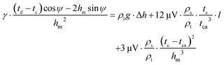
Fig. 2 shows a schematic of the meniscus. The meniscus at the die top is in a state of pressure equilibrium. The pressure difference between the liquid in the meniscus and the gas in the furnace comprises three components: ΔP1 is the hydrostatic pressure that drives the liquid in the capillary to rise; ΔP2 is the pressure loss due to liquid flowing in the capillary; and ΔP3 is the pressure loss due to horizontal flow of the liquid at the die top. The curvature related to the pressure difference can be represented by the Laplace equation:22| | | γ/R = ΔP1 + ΔP2 + ΔP3 | (10) |
| |  | (11) |
where γ is the surface tension, R is the meniscus vertical radius of curvature, t is the thickness, ψ is the growth angle, hm is the meniscus height, ρ is the density, Δh is the distance between the die top and the crucible melt, µ is the viscosity, V is the growth rate, and lca is the capillary canal length. The subscripts d, c and ca are the die, crystal and the capillary canal, respectively.
 |
| | Fig. 2 Geometrical parameters of the meniscus and thermal balance at the solid–liquid interface. | |
In the energy conservation equation at the solid–liquid interface, Q1 is the heat conducted by the solid, Q2 is the heat conducted by the liquid, Q3 is the heat radiation in the meniscus, and Q4 is the latent heat of solidification.
| | | ksgradsT = klgradlT + εσ(T4 − Tm4) + ρsVLs | (13) |
| | 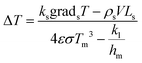 | (14) |
where grad
sT is the temperature gradient in the solid, grad
lT is the temperature gradient in the liquid,
ε is the emissivity,
σ is the Stefan Boltzmann constant,
Ls is the latent heat of solidification,
T is the temperature at the die top, and
Tm is the melting point. The liquid temperature gradient grad
lT varies linearly with the meniscus height
hm.
22 Δ
T =
T −
Tm, the overheating Δ
T is defined by the temperature difference between the die top and the melting point. Substituting the simulated solid temperature gradient into
eqn (11) and (14) yields the relationship between the growth rate
V, the meniscus height
hm, and the overheating Δ
T, thereby facilitating the selection of an appropriate pulling speed.
3. Results and discussion
The temperature gradient serves as the driving force for crystal growth. To ensure effective crystal growth, it is necessary for the magnitude of the temperature gradient to be appropriately matched to the required driving force. Furthermore, the temperature distribution on the die surface significantly influences the stability of crystal growth. Therefore, we optimize the thermal insulation configuration near the die top region. Inside the furnace, the die is located at the center of the crucible, with the die top slightly higher than the crucible cover. As shown in Fig. 3, we define two structures: structure A, which lacks insulation material on its crucible cover; and structure B, which is equipped with carefully placed insulation material on its crucible cover. The graphite carbon felt covers the entire upper surface of the crucible cover, with dimensions of 500 × 80 mm. The thermal insulation material employed in structure B is graphite carbon felt. To prevent any reaction between the graphite carbon felt and the molybdenum crucible cover, tungsten sheets are inserted between them.
 |
| | Fig. 3 Diagram of structures A and B, where only the crucible cover, crucible, die, and insulation materials are shown. | |
Fig. 4 illustrates the temperature field distribution in the core region, including the die, crucible, and melt. In view of the biaxial symmetry of this region, only a quarter of it is depicted in the figure. As shown in Fig. 4(b), the application of insulating carbon felt increased the overall melt temperature by approximately 30 K. This temperature rise demonstrated that at constant heater power, the carbon felt could reduce the power requirement for raw material melting, thereby improving energy efficiency. The comparative analysis of die temperature distributions in Fig. 4(a) and (b) demonstrates that the introduction of insulating carbon felt induces significant thermal modifications. The die region immersed in the melt exhibits a marked temperature increase, while the axial temperature gradient along the die height becomes substantially enhanced. Meanwhile, the localized high-temperature zone observed in Structure A between the melt surface and crucible cover is effectively eliminated in Structure B. This phenomenon stems from radiative heat transfer between the uninsulated crucible wall and the die surface in the same horizontal plane, which generates the localized hot zone depicted in Fig. 4(a). Following the application of insulating carbon felt, the increase in melt temperature elevated the temperature of the immersed die region correspondingly, homogenizing the thermal distribution between the melt surface and crucible cover, thereby eliminating the localized hot zone.
 |
| | Fig. 4 Temperature distribution of the die, crucible, and melt: (a) without carbon felt, (b) with carbon felt. | |
Fig. 5 depicts the temperature field distribution on the die top surface, using a quarter-die structure. The thermal profile exhibits a distinct radial gradient, with the maximum temperature (Point A: die center) decreasing gradually toward the periphery (Point B: die edge). In the EFG furnace, the resistance heaters mounted on the sidewalls are positioned in close proximity to both the crucible and die. When there is no insulating carbon felt on the crucible cover, thermal radiation from the heater primarily heats the crucible cover and die top surface. The die top edge exhibits accelerated cooling via heat exchange with the surrounding environment, consequently serving as the primary heat dissipation pathway. Consequently, a significant temperature difference emerges between the center and the edge of the die top surface, as shown in Fig. 5(a), which is 7.29 K. While the application of insulation is evidently effective, the extent of its impact is closely tied to the thickness of the carbon felt. To precisely optimize the thermal insulation configuration and achieve the desired temperature distribution, a systematic investigation into the influence of carbon felt thickness is necessary.
 |
| | Fig. 5 Temperature distribution at the die top surface: (a) without carbon felt, (b) 20 mm thick carbon felt, (c) 40 mm thick carbon felt, (d) 50 mm thick carbon felt, (e) 60 mm thick carbon felt, and (f) temperature difference at the die top surface. | |
To further study the impact of carbon felt thickness on temperature distribution, simulation results of different thicknesses applied to the die top are shown in Fig. 5(b–e). With a 20 mm thick carbon felt, this difference decreased to 3.42 K. A more substantial improvement was observed at 40 mm thickness, where the temperature difference was reduced to 2.43 K. Further increasing the thickness to 50 mm and 60 mm resulted in only marginal reductions to 2.37 K and 2.25 K, respectively. The results of temperature difference between Point A Point B (ΔTA–B) at the die top surface and the trend of temperature variation are shown in Fig. 5(f). This trend indicates a diminishing marginal effect: carbon felt's beneficial effect on reducing the surface temperature difference becomes less significant as the carbon felt thickness increases beyond 40 mm. Thus, the 40 mm thick carbon felt already achieves an obvious improvement in radial temperature distribution, effectively minimizing thermal stress concentration and suppressing crystal defects, while additional thickness offers limited further benefit.
During the crystal growth process, the radial temperature distribution has a significant impact on the growth stability and defect formation, and this influence is particularly pronounced during the shoulder stage. Although the pulling rate remains constant throughout the shoulder stage, the shoulder area expands exponentially with time, resulting in a rapid increase in the crystal mass. As the shoulder area expands, the heat dissipation rate of the shoulder also increases. This leads to an increase in thermal stress within the crystal, thereby increasing the risk of cracking. Consequently, it is necessary to control the radial temperature distribution, keeping it at a relatively low level and ensuring a uniform distribution. Along the die top surface, an excessively large temperature difference will accelerate the lateral growth rate of the crystal, inducing the flat shoulder phenomenon and subsequently degrading the crystal quality. By applying insulating carbon felt, the temperature difference on the die top surface is reduced to one-third of that without the application, effectively suppressing the formation of crystal cracking and the flat shoulder phenomenon. The axial temperature data within a 3 cm range above the die top surface are extracted, and the results are illustrated in Fig. 6. As depicted in Fig. 6(a), with the increase of the thickness of the carbon felt, the temperature near the die top surface decreases. The temperature was lower than that without the use of carbon felt, but there were differences. The main point is that after the thickness of the carbon felt exceeded 40 mm, further increasing the thickness to 50 mm or 60 mm resulted in a smaller decrease in temperature as Z increased.
 |
| | Fig. 6 (a) Axial temperature distribution above the die, and (b) axial temperature gradient above the die (Z = 0 denotes the center of die top surface). | |
Fig. 6(b) displays the axial temperature gradient. When the thickness of the carbon felt is gradually increased to 40 mm, the gradient increases from −6.13 K cm−1 to −10.95 K cm−1, thereby enhancing the driving force for crystallization. When we continue to increase the thickness of the carbon felt to 60 mm, it can be observed that the gradient decreases to −8.47 K cm−1. This might be due to the restricted axial heat dissipation path when the carbon felt was too thick. Consequently, the addition of appropriate thickness thermal insulation carbon felt facilitates the growth of thick and wide crystals with uniform shapes and fewer cracks.
We thoroughly analyze the key role of controllable parameters in the crystal growth process and their impact on growth results, in order to more accurately regulate and optimize the crystal growth conditions. Two critical controllable parameters are the overheating at the die top and the pulling speed in the process of crystal growth. After modifying the design of the thermal insulation device, we conducted simulations of the temperature field and incorporated the simulated temperature gradient into the heat and pressure balance equations within the meniscus. By substituting the axial temperature gradient of structure B into the above formula (11) and (14), the relationship between the growth rate and the overheating is derived and recorded in Fig. 7. As shown in Fig. 7, ΔT decreases as the growth rate V increases. Overheating ΔT represents the temperature difference between the melting point and the die top, and the pulling speed can be approximated as the crystal growth rate V.
 |
| | Fig. 7 Relationship between ΔT and growth rate V. | |
As illustrated in Fig. 7, the maximum growth rate of the crystal is constrained. An excessively rapid pulling speed can result in a negative value of ΔT. When the pulling speed exceeds 4.5 µm s−1, the value of ΔT becomes zero, resulting in the interface freezing on the die. Therefore, during the growth phase, a pulling speed near the center of the appropriate range should be selected, for instance 3.0 µm s−1. In practical crystal growth processes, the introduction of low-temperature seeds effectively enhances the axial temperature gradient near the die top surface, thereby increasing the theoretical maximum growth rate.
These calculations provide crucial guidance for crystal growth processes, enabling a more scientific approach to parameter regulation, enhancing controllability, and substantially reducing the costs associated with multiple experiments. The crystal grown using this 40 mm thick carbon felt thermal insulation device and the specified process parameters is shown in Fig. 8. The transparency of the as-grown crystal is good, but there is a bubble layer on its surface. As depicted in Fig. 8, there are lines on the crystal surface, reflecting the diffusion paths of microbubbles within the melt onto the die. The specific mechanisms underlying these phenomena require further investigation.
 |
| | Fig. 8 Photograph of the Yb:YAG crystal grown using the EFG method. | |
In order to further characterize the luminescence properties of the crystal, we measured the XEL spectra and decay times using an Edinburgh Instrument FLS1000 photoluminescence spectrometer coupled with an X-ray generator and a 213 nm laser, and both the EFG-grown and Cz-grown crystal samples were cut and polished to identical dimensions of 10 × 10 × 1 mm3. The Cz method is currently the primary technique for growing Yb:YAG crystals, which exhibit excellent optical properties. In this study, the Cz method was also utilized to grow Yb:YAG crystals. Fig. 9 shows the XEL spectra and decay time profiles of Yb:YAG crystals grown using the EFG and Cz method. At room temperature, it can be seen that the XEL spectral line of the EFG-grown crystal is basically consistent with that of the Cz-grown crystal. The main luminescence peak at 335 nm corresponds to the charge transfer (CT) state transition to 2F7/2, and the weaker luminescence band near 500 nm is caused by the CT state transition to 2F5/2.24 The decay curves are fitted using a single-term exponential function. Under the excitation of a 213 nm laser, the decay times of the EFG-grown and Cz-grown crystals at 330 nm are comparable, which are 1.45 ns and 1.44 ns respectively. This fully demonstrates that the crystals grown using the EFG method exhibit comparable luminescence characteristics to those grown using the Cz method.
 |
| | Fig. 9 (a) XEL spectra and (b) decay time of the Yb:YAG crystals grown using the EFG and Cz method. | |
4. Conclusions
In order to establish an appropriate temperature field, we installed different thicknesses of graphite carbon felt on the crucible cover and conducted numerical simulation calculations. The results demonstrate that applying a 40 mm thick carbon felt on the die top can effectively optimize the temperature distribution. Specifically, the axial temperature gradient is increased to −10.95 K cm−1, while the radial temperature difference is reduced to 2.43 K. This modification significantly enhances the axial temperature gradient, providing the essential driving force for crystal growth. Moreover, the uniform temperature distribution across the die top surface effectively prevents thermal stress concentration and cracking. Furthermore, we refined and adjusted the growth process parameters to optimize the crystal quality. Through the accurate calculation of the meniscus, we established the relationship between the overheating at the die top and the growth rate, thereby providing a reference range of pulling speeds suitable for the crystal growth process. Consequently, we successfully grew the large-sized and high-quality Yb:YAG crystal. Subsequent tests on the annealed crystal samples, including XEL and decay time measurements, revealed that the luminescence properties of the EFG-grown crystal are consistent with those of the Cz-grown crystal. Furthermore, given the high similarity in thermophysical properties—such as the melting point, thermal conductivity, and melt viscosity—between Yb:YAG and other rare-earth ion-doped yttrium aluminum garnet (RE:YAG) crystals, the thermal field optimization strategy proposed in this study is widely applicable. The established correlation between the insulation configuration and temperature gradient regulation can be theoretically extended to the EFG growth of other garnet systems, providing generalizable guidelines for achieving high-quality growth within this class of materials. This achievement lays a foundation for the research and development of growing other rare earth ion-doped garnet crystals using the EFG method.
Author contributions
The manuscript was collaboratively written by all authors, and the final version was approved by each author.
Conflicts of interest
There are no conflicts to declare.
Data availability
The data that support the findings of this study are available from the corresponding author, Mingyan Pan, upon reasonable request.
Acknowledgements
The authors acknowledge the Youth Innovation Promotion Association, Chinese Academy of Sciences (CAS) (No. 2023254), and the Strategic Priority Research Program of the Chinese Academy of Sciences, Grant No. XDA 0380000.
Notes and references
- W. Schneider, A. Ryabov, C. Lombosi, T. Metzger, Z. Major, J. A. Fulop and P. Baum, 800-fs, 330-µJ pulses from a 100-W regenerative Yb:YAG thin-disk amplifier at 300 kHz and THz generation in LiNbO3, Opt. Lett., 2014, 39, 6604–6607 Search PubMed.
- K. Xiao, X. Yuan, X. Jiang, X. Yan, Z. Wang, M. Li, J. Zheng and W. Zheng, Research Status of Conceptual Design of Diode-Pumped Solid-State Laser Driver for LIFE, Laser Optoelectron. Prog., 2015, 52, 040001–040010 CrossRef.
- G. Bressi, G. Carugno, E. Conti, C. Del Noce and D. Iannuzzi, New prospects in scintillating crystals, Nucl. Instrum. Methods Phys. Res., Sect. A, 2001, 461, 361–364 Search PubMed.
- L. F. Johnson and J. E. Geusic, Vanuiter.Lg, Coherent oscillations from Tm3+, Ho3+, Yb3+, and Er3+ ions in yttrium aluminum garnet (threshold reduction by energy transfer E), Appl. Phys. Lett., 1965, 7, 127 CrossRef CAS.
- D. P. Bour, G. A. Evans and D. B. Gilbert, High-power conversion efficiency in a strained InGaAs/AlGaAs quantum well laser, J. Appl. Phys., 1989, 65, 3340–3343 CrossRef CAS.
- J. Dong, A. Shirakawa, K.-I. Ueda, H. Yagi, T. Yanagitani and A. A. Kaminskii, Efficient Yb3+:Y3Al5O12 ceramic microchip lasers, Appl. Phys. Lett., 2006, 89, 091114 CrossRef.
- A. Giesen, H. Hugel, A. Voss, K. Wittig, U. Brauch and H. Opower, Scalable concept for diode-pumped high-power solid-state lasers, Appl. Phys. B:Lasers Opt., 1994, 58, 365–372 CrossRef.
- N. Guerassimova, N. Garnier, C. Dujardin, A. G. Petrosyan and C. Pédrini, X-ray-excited charge transfer luminescence in YAG:Yb and YbAG, J. Lumin., 2001, 94, 11–14 Search PubMed.
- X. Li, G. Yang, J. Han, Y. Wang, H. Bi and X. Xu, Growth of high quality φ10 inch Yb:YAG laser crystal by Czochralski method, J. Synth. Cryst., 2023, 52, 547–549 Search PubMed.
- H. E. Labelle, EFG, The invention and application to sapphire growth, J. Cryst. Grow., 1980, 50, 8–17 CrossRef CAS.
- H. Aida, K. Nishiguchi, H. Takeda, N. Aota, K. Sunakawa and Y. Yaguchi, Growth of β-Ga2O3 Single Crystals by the Edge-Defined, Film Fed Growth Method, Jpn. J. Appl. Phys., 2008, 47, 8506–8509 CrossRef CAS.
- C. Stelian, N. Barthalay and T. Duffar, Numerical investigation of factors affecting the shape of the crystal-melt interface in edge-defined film-fed growth of sapphire crystals, J. Cryst. Grow., 2017, 470, 159–167 CrossRef CAS.
- C. Le, Z. Li, W. Mu, Z. Jia and L. Liu, 3D numerical design of the thermal field before seeding in an edge-defined film-fed growth system for β-Ga2O3 ribbon crystals, J. Cryst. Grow., 2019, 506, 83–90 CrossRef CAS.
- L. Zhang, M. Pan, R. Tian, J. Sun, J. Mao, W. Kong, B. Jiang, W. Ji and H. Qi, Rapid Growth of a Yb:YAG Slab Crystal with Superior Laser Properties by the Edge-Defined Film-Fed Growth Method, Cryst. Growth Des., 2024, 24, 1959–1968 CrossRef CAS.
- W. W. Mullins and R. F. Sekerka, Morphological stability of a particle growing by diffusion or heat flow, J. Appl. Phys., 1963, 34, 323 Search PubMed.
- E. M. Nunes, M. H. N. Naraghi, H. Zhang and V. Prasad, A volume radiation heat transfer model for Czochralski crystal growth processes, J. Cryst. Grow., 2002, 236, 596–608 Search PubMed.
- D. Schwabe, R. R. Sumathi and H. Wilke, An experimental and numerical effort to simulate the interface deflection of YAG, J. Cryst. Grow., 2004, 265, 440–452 CrossRef CAS.
- C. W. Lan and C. J. Chen, Dynamic three-dimensional simulation of facet formation and segregation in Bridgman crystal growth, J. Cryst. Grow., 2007, 303, 287–296 CrossRef CAS.
- J. Banerjee and K. Muralidhar, Role of internal radiation during Czochralski growth of YAG and Nd:YAG crystals, Int. J. Therm. Sci., 2006, 45, 151–167 CrossRef CAS.
- J. Quan, G. Ke, Y. Zhang, J. Liu and J. Huang, Study on Growth Interface of Large Nd:YAG Crystals, Crystals, 2023, 13, 970 CrossRef CAS.
- A. Golubovic, S. Nikolic, R. Gajic, S. Duric and A. Valcic, The growth of Nd:YAG single crystals, J. Serb. Chem. Soc., 2002, 67, 291–300 CrossRef CAS.
- L. Carroz and T. Duffar, Tuning the sapphire EFG process to the growth of Al2O3/YAG/ZrO2:Y eutectic, J. Cryst. Grow., 2018, 489, 5–10 CrossRef CAS.
- C.-H. Chen, J.-C. Chen, C.-W. Lu and C.-M. Liu, Numerical simulation of heat and fluid flows for sapphire single crystal growth by the Kyropoulos method, J. Cryst. Grow., 2011, 318, 162–167 CrossRef CAS.
- R. Tian, L. Zhang, M. Pan and H. Qi, Growth and Spectral Properties of Si4+ Co-Doped Yb:YAG Single Crystal, J. Synth. Cryst., 2021, 50, 1957–1962 CAS.
|
| This journal is © The Royal Society of Chemistry 2026 |
Click here to see how this site uses Cookies. View our privacy policy here. 
 Open Access Article
 This Open Access Article is licensed under a Creative Commons Attribution-Non Commercial 3.0 Unported Licence
 ab,
Bowen
Jiang
ac,
Lu
Zhang
ab,
Shaoqing
Cui
ab,
Yexi
Huang
a,
Ning
Jia
a,
Hongji
Qi
ad and
Mingyan
Pan
*a
ab,
Bowen
Jiang
ac,
Lu
Zhang
ab,
Shaoqing
Cui
ab,
Yexi
Huang
a,
Ning
Jia
a,
Hongji
Qi
ad and
Mingyan
Pan
*a


