
 Open Access Article
 This Open Access Article is licensed under a Creative Commons Attribution-Non Commercial 3.0 Unported Licence
Morphology-engineered α-MoO3 nanostructures via MoS2 transformation for high-performance supercapacitors
Ahmed A.R.
Abdel-Aty
a,
Mohammed Mosaad
Awad
a,
Olfa
Kanoun
b and
Ahmed S.G.
Khalil
 *cd
*cd
aInstitute of Basic and Applied Science, Egypt-Japan University of Science and Technology (E-JUST), 179 New Borg El-Arab City, Alexandria, Egypt
bProfessorship of Measurement and Sensor Technology, Chemnitz University of Technology, Reichenhainer Str. 70, 09126 Chemnitz, Germany
cEnvironmental and Smart Technology Group, Faculty of Science, Fayoum University, 63514, Fayoum, Egypt. E-mail: asg05@fayoum.edu.eg
dEvoSmarTec GmbH, Alfredstr. 81, 45130 Essen, Germany
First published on 11th December 2025
Abstract
We report a morphology-engineering strategy to enhance supercapacitor performance by transforming hydrothermally synthesized 1T/2H-MoS2 nanosheets into α-MoO3 nanoflakes through controlled thermal annealing. For comparison, α-MoO3 nanoplates and nanofibers were also prepared via calcination and hydrothermal methods, respectively. Comprehensive structural, morphological, and surface analyses confirmed the formation of phase-pure orthorhombic α-MoO3 with distinct morphologies. Electrochemical evaluation revealed that the nanoflake morphology exhibited the highest specific capacitance of 755 F g−1 at a scan rate of 5 mV s−1, along with the lowest charge-transfer resistance of 0.14 Ω at a current density of 1 A g−1 in 1 M H2SO4, outperforming both the nanoplate and nanofiber counterparts. The superior performance is attributed to the high electrochemically active surface area, abundant accessible redox sites, and efficient ion diffusion pathways provided by the nanoflakes. This work demonstrates a simple, scalable route for producing high-performance α-MoO3 electrodes, offering valuable insights into morphology–property relationships for next-generation energy storage devices.
1. Introduction
The rapid development of hybrid electric vehicles, power systems, and portable electronics has increased the demand for efficient energy storage systems.1,2 Among them, supercapacitors have gained significant attention because of their high power and energy density, long cycle life, environmental stability, and low maintenance requirements.3,4 Supercapacitors are classified as electrochemical double-layer capacitors (EDLCs) or pseudocapacitors, depending on their energy storage mechanism.5,6 EDLCs store energy by adsorption of ionic charges on porous carbon-based electrodes, but their capacitance is limited by the surface area of the electrode material.7 In contrast, pseudocapacitors store energy through fast, reversible redox reactions at the surface of active materials, leading to much higher specific capacitance.8,9 This makes pseudocapacitors an excellent choice for the next generation of energy storage devices with higher energy and power densities, longer lifetime, and better sustainability. The overall performance of a supercapacitor depends strongly on the choice of electrode material. In recent decades, many new nanostructures have been reported for supercapacitor applications, including carbon materials, conductive polymers, and transition metal compounds such as oxides, nitrides, and sulfides, with laser-induced graphene (LIG) emerging as a particularly promising candidate due to its high conductivity and porous architecture.10 The search for optimal electrode materials is still ongoing.11In this context, the design and fabrication of two-dimensional (2D) materials for environmental and energy applications has become an active research area, leading to major advances in the last decade.12,13 Metal oxides such as MnO2, MoO3, Bi2O3, and Fe2O3 have unique functionalities that make them suitable for high-performance electrodes and for dye removal.14,15 Their ability to undergo fast, reversible redox reactions result in higher specific capacitance, enhancing energy density, power delivery, and device efficiency.16 Mo-based oxides are particularly interesting because of their multiple oxidation states and high electrochemical activity.17,18
Molybdenum disulfide (MoS2), a 2D transition metal dichalcogenide (TMD), has high ionic conductivity and abundant active sites due to its phase- and layer-dependent properties.19 Its layered S–Mo–S structure allows easy cation intercalation/deintercalation during electrochemical processes, increasing ion storage capacity.20 For example, Bin Li et al.21 reported inkjet-printed MoS2 micro-supercapacitors with layer-dependent capacitive behavior, achieving a maximum areal capacitance of 175 µF cm−2 for 10-layer coatings, along with energy and power densities of 0.215 mWh cm−3 and 0.079 W cm−3, respectively. Xiumei Geng et al.22 prepared multilayer metallic MoS2 (M-MoS2) nanosheets with water layers, obtaining a specific capacitance of 380 F g−1 at 5 mV s−1. The water layers improved electron transport and ion diffusion. Moreover, integrating MoS2 with conductive frameworks such as laser-induced graphene (LIG) has recently emerged as an effective strategy to overcome its intrinsic limitations. Mensah et al. demonstrated that engineering a well-defined MoS2/LIG interface significantly enhances charge transport, electrolyte accessibility, and structural stability, resulting in markedly improved supercapacitor performance. Their findings further highlight the potential of MoS2-based hybrid architectures for next-generation high-energy, flexible microsupercapacitors.23
Despite such progress, MoS2 suffers from poor rate capability, volume expansion during cycling, and limited stability. These drawbacks can be reduced by combining MoS2 with metal oxides, carbon, or polymers.
Molybdenum oxide (MoO3) is another promising 2D material because of its rich redox chemistry, high thermal and chemical stability, and layered crystal structure.24,25 MoO3 exists mainly in three polymorphs: orthorhombic α-MoO3 (thermodynamically stable), and metastable β-MoO3 and h-MoO3. The layered α-MoO3 has strong anisotropy and can form low-dimensional structures. However, its low electrical conductivity and slow reaction kinetics limit its performance. Nanoscale 1D and 2D MoO3 can overcome these problems by providing a high surface-to-volume ratio and better conductivity.26 Layered α-MoO3 has been synthesized by hydrothermal synthesis,27 electrodeposition,28 chemical vapor deposition (CVD),29 and thermal evaporation.30 Each method has drawbacks. Hydrothermal synthesis and electrodeposition can have material limitations and complex reaction conditions, while CVD and thermal evaporation are costly because they require vacuum systems and controlled gas flows. For example, Pujari et al. prepared MoO3 microrod thin films by chemical bath deposition, achieving 194 F g−1 specific capacitance, 1200 W kg−1 power density, and 7.33 Wh kg−1 energy density. The 2D layered α-MoO3 structure also offers high surface area for ion diffusion and charge storage.31 These properties make α-MoO3 a strong candidate for next-generation supercapacitors and batteries, but a simpler and more scalable synthesis method is still needed.
In this work, we developed morphology-tuned α-MoO3 nanoflakes by thermal annealing of hydrothermally synthesized 1T/2H-MoS2 nanosheets. For comparison, α-MoO3 nanoplates and nanofibers were synthesized by calcination and hydrothermal methods. We systematically investigated the structural, morphological, optical, electrical, and surface properties of the products, and evaluated their electrochemical performance as supercapacitor electrodes. The results provide new insights into how synthesis methods affect the morphology and performance of α-MoO3 for energy storage applications.
2. Experimental
2.1. Materials
Ammonium molybdate ((NH4)6Mo7O24·4H2O) was purchased from SUVCHEM, India. Thiourea (CH4N2S) was obtained from ADVENT, India. Nitric acid (HNO3) and citric acid monohydrate were purchased from Loba Chemie, India. All chemicals were used without further purification.2.2. Synthesis of 1T/2H-MoS2 nanosheets by the hydrothermal method
MoS2 nanosheets (S0) were prepared by a hydrothermal method. In a typical process, 76.5 mL of deionized (DI) water was used to dissolve 2.47 g of ammonium molybdate and 0.76 g of Thiourea at a Mo![[thin space (1/6-em)]](https://www.rsc.org/images/entities/char_2009.gif) :S molar ratio of 1:5 under continuous stirring at 400 rpm. The solution was transferred into a 170 mL Teflon-lined autoclave, filled to 45% of its capacity, and heated at 200 °C for 24 h. After cooling to room temperature (25 °C), the black precipitate was collected, centrifuged at 4000 rpm for 40 min, and washed several times with ethanol and DI water. The product was dried at 80 °C for 12 h, yielding 70% 1T/2H-MoS2 (S0).
:S molar ratio of 1:5 under continuous stirring at 400 rpm. The solution was transferred into a 170 mL Teflon-lined autoclave, filled to 45% of its capacity, and heated at 200 °C for 24 h. After cooling to room temperature (25 °C), the black precipitate was collected, centrifuged at 4000 rpm for 40 min, and washed several times with ethanol and DI water. The product was dried at 80 °C for 12 h, yielding 70% 1T/2H-MoS2 (S0).
2.3. Synthesis of α-MoO3 by thermal annealing of 1T/2H-MoS2 nanosheets
α-MoO3 nanoflakes (S1) were obtained by thermal annealing of MoS2 nanosheets at 400 °C for 2 h in a muffle furnace under air. The MoS2 was oxidized to α-MoO3, producing a grey powder.2.4. Synthesis of α-MoO3 by surfactant-free chemical method
α-MoO3 nanoplates (S2) were synthesized via a calcination method. First, 4 g of ammonium molybdate dihydrate was dissolved in 100 mL of DI water and stirred at 60 °C for 30 min at 700 rpm. The solution was then heated at 120 °C in an oven to remove water, forming a light green powder. The powder was calcined at 400 °C for 30 min in air to obtain grey α-MoO3 nanoplates (S2).2.5. Synthesis of α-MoO3 by Teflon-lined autoclave hydrothermal
α-MoO3 nanofibers (S3) were prepared by a hydrothermal method, as shown in Scheme 1. In this process, 0.618 g of ammonium molybdate dihydrate was suspended in 120 mL of DI water and stirred at 60 °C, 400 rpm. Then, 0.315 g of citric acid was added, followed by 0.5 mL of nitric acid, added dropwise over 30 min while stirring. The homogeneous solution was transferred to a Teflon-lined autoclave (filled to 60% capacity) and heated at 180 °C for 12 h. The product was washed with ethanol and water, dried for 12 h, and collected as α-MoO3 nanofibers (S3).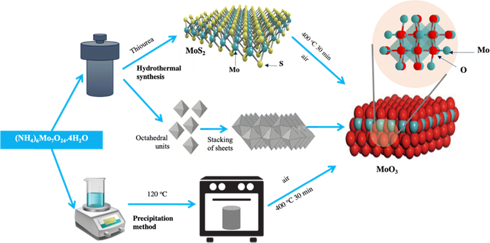 | ||
| Scheme 1 Schematic diagram of fabrication of 1T/2H-MoS2 (S0) and α-MoO3 (S1, S2, S3) samples. | ||
2.6. Materials characterization
The morphology of α-MoO3 nanostructures was examined using a field emission scanning electron microscope (FESEM, ZEISS Sigma 500 VP) equipped with an energy-dispersive X-ray (EDX) detector, and transmission electron microscopy (TEM, JEOL 1200). X-ray diffraction (XRD) patterns were obtained using Cu Kα radiation (λ\lambdaλ = 1.54056 Å) on a PANalytical Empyrean diffractometer at room temperature. X-ray photoelectron spectroscopy (XPS) measurements were carried out on a K-ALPHA instrument (Thermo Fisher Scientific, USA) using monochromatic Al Kα radiation. Raman spectra were recorded with a WITec α 300 RA confocal Raman microscope using a 532 nm Nd:YAG laser. Surface area measurements were performed using the Brunauer–Emmett–Teller (BET) method with N2 adsorption–desorption isotherms at 77 K (TriStar system). UV-Vis spectra were measured using a Cary 60 Agilent spectrophotometer. Attenuated total reflection infrared (ATR-IR) spectra were obtained for surface functional group analysis. Zeta potential and particle size distributions were measured using a Zetasizer Nano (Malvern, UK).2.7. Electrochemical characterization
Electrochemical tests were performed using a CHI 660 workstation in a three-electrode configuration. A slurry was prepared by mixing MoO3 powder, carbon black, and polyvinylidene fluoride (PVDF) in a mass ratio of 80:10:10 with N-methyl-2-pyrrolidone (NMP) as the solvent, followed by sonication for 1 h. The slurry was coated on graphite foil (1 cm2), dried at 120 °C for 11 h in a vacuum oven, and used as the working electrode. An Ag/AgCl electrode and platinum foil served as the reference and counter electrodes, respectively. The electrolyte was 1 M H2SO4.
Cyclic voltammetry (CV) was performed at scan rates from 5 to 100 mV s−1 in the 0–1 V range. Galvanostatic charge–discharge (GCD) measurements were carried out at current densities from 1 to 5 A g−1. Electrochemical impedance spectroscopy (EIS) was performed in the frequency range 105–10−2 Hz. The specific capacitance Cs was calculated from the CV and GCD data using the following equations:
 | (1) |
 | (2) |
3. Results and discussion
3.1. Structural and morphological characterization
The FE-SEM images of the S0 and S1 were analyzed at lower and higher magnification, and the findings are illustrated in Fig. 1. The images displayed in Fig. 1a–c show that S0 is composed of homogeneous spherical nanoflowers with an average lateral dimension of 250 nm, and nanosheets dispersed randomly in the sample. These nanosheets are approximately 150 nm in size. Fig. 1d–f shows the morphology of S1. It is observed that the morphology changes from a flower-like structure to a nanoflakes structure, demonstrating a complete conversion to molybdenum trioxide. Based on the FE-SEM micrograph, the flake thickness is estimated to be around 30 nm. Each flake is around 200 × 300 nm in size, arranged one layer over the other. This nanoflake-like structure may also contain narrow sub-flakes interspersed within it. Thermal annealing at 400 °C is likely responsible for the one-directional elongation. FE-SEM micrographs show that these elongated stacked layers are weakly connected. The sample length extends from 0.8 µm to 1 µm, with a thickness of 200–300 nm. The morphology of the as-obtained α-MoO3 sample synthesized by the surfactant-free chemical method (S2) and hydrothermal method (S3) is depicted in the FE-SEM images shown in Fig. 2, which display nanoplates38 and a fiber-like structure, respectively. Fig. 2a–c shows the FE-SEM micrographs of S2 at different resolutions. It clearly reveals a compact α-MoO3 agglomerated hierarchical nanoplate structure. Fig. 2d–f shows typical high and low magnification FE-SEM micrographs of S3. These images show a uniform and smooth surface with fiber-like morphology. The sample consists of nearly 100% fibers, with lengths in the micrometer range. The fibers have a thickness of approximately 200 nm and possess a rectangular cross-section. | ||
| Fig. 1 FE-SEM micrographs of (a) S0 with flower-like morphology, (b) S1 with plate-like morphology. | ||
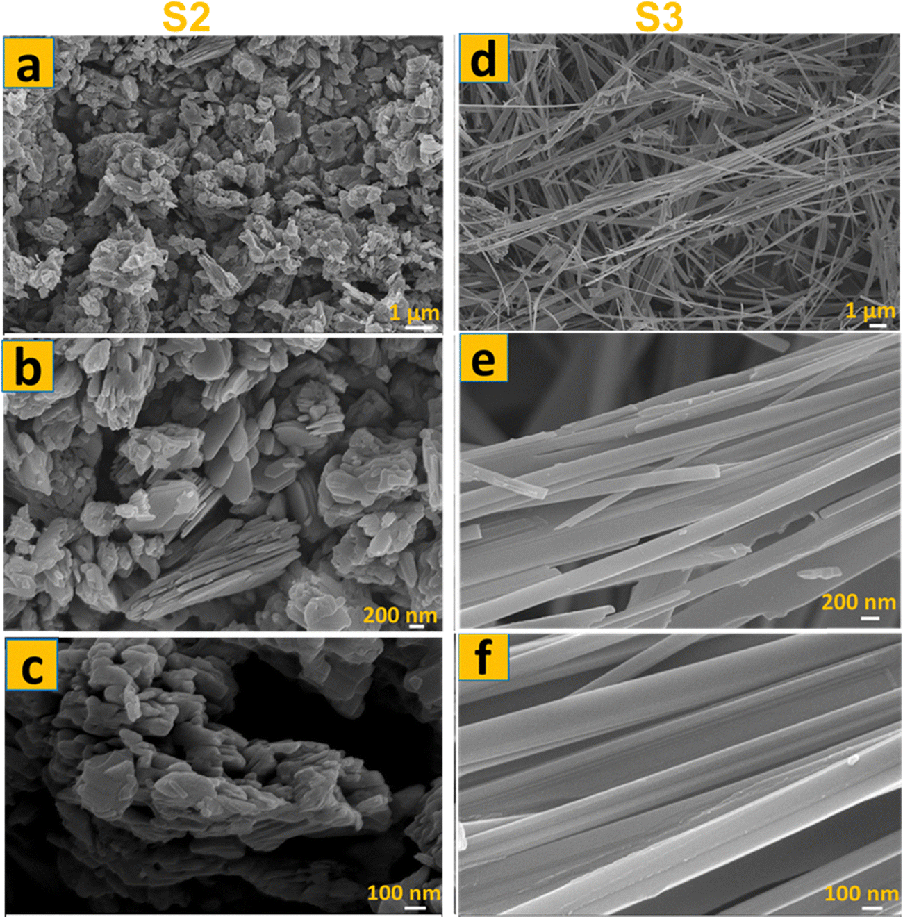 | ||
| Fig. 2 FE-SEM micrographs of (a) S2 with hierarchical nanoplatelets morphology, (b) S3 with fiber-like morphology. | ||
Fig. 3a shows the XRD patterns of the prepared samples using Cu Kα radiation at a wavelength of 1.54 Å to assess their crystal structure features. S0 has unique diffraction peaks closely matching those of JCPDS Card no. 37-1492. Peaks for the (002), (100), and (110) planes appear at angles of 13.2°, 32.7°, and 58.3°, respectively. Interestingly, the primary peak appears at a lower angle than the hexagonal molybdenum sulfide JCPDS Card no. 01-075-1539, indicating that the distance between the MoS2 basal planes has increased.32 The presence of broad peaks in the sample's XRD pattern suggests that the material possesses a nanostructured nature. After the thermal annealing process for the 1T/2H-MoS2 sample (S1), new peaks at 12.7°, 23.3°, 25.7°, 27.3°, 33.8°, and 55.3° are observed, representing the (020), (110), (040), (021), (111), (060), and (002) reflections with d-spacings of 6.9, 3.8, 3.4, 3.2, 2.65, 2.3, and 1.65 Å, which match JCPDS Card no. 21-0569 for MoO3 orthorhombic crystal, confirming that MoS2 has been completely converted into MoO3.33 The orthorhombic crystalline structure of MoO3 is confirmed to be present in the synthesized material by the XRD pattern of S2, which shows large sharp peaks that closely resemble those of the converted 1T/2H-MoS2. Other smaller peaks also show good matching. Importantly, no peaks matching other MoO3 phases were found, suggesting that the sample did not include any additional crystalline phases. The XRD patterns of α-MoO3 fibers (S3) show characteristic diffraction peaks matching for orthorhombic MoO3, with major peaks at 12.74°, 25.88°, and 39.09°, with higher intensities than those corresponding to the (020), (040), and (060) planes, respectively. This might be due to the presence of a layered crystalline structure or anisotropic growth of the oxide.
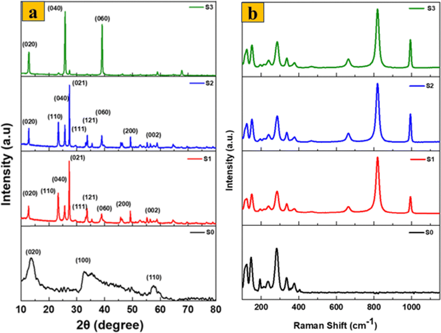 | ||
| Fig. 3 (a) XRD pattern of S0 and α-MoO3 nanostructures, and (b) Raman spectra of S0 and α-MoO3 nanostructures. | ||
The Raman spectra of S0, S1, S2, and S3 samples are presented in Fig. 3b. The Raman spectrum of S0 exhibits six distinctive peaks at 147, 197, 283, 336, 377, and 404 cm−1. Among them, peaks at 149, 197, and 336 cm−1 may be identified as the Mo–Mo stretching vibration and the phonon mode typical of 1T-MoS2. However, sample S1 shows only peaks corresponding to pure MoO3. The peak at 219 cm−1 represents the translation mode of rigid chains. The (B2g, B3g) modes at 283.7 cm−1 (O![[double bond, length as m-dash]](https://www.rsc.org/images/entities/char_e001.gif) MoO) are the wagging modes of vibrations caused by the presence of terminal oxygen atoms. The vibrational mode at 665.8 cm−1 (B2g, B3g) indicates the asymmetric stretching of triply coordinated (Mo3–O) edge-sharing oxygen atoms. O–Mo–O has a bending mode at 337 cm−1, and a peak at 819.1 cm−1 (Mo2–O) and 993 cm−1 (Mo6+O) indicate symmetric and asymmetric stretching of terminal oxygen atoms, respectively. Alternatively, S2 and S3 have roughly matching vibrational peak locations, emphasizing their structural similarities. Three distinct peaks are seen at 995, 822, and 666 cm−1. The 995 cm−1 peak represents the vibration of asymmetric terminal O atoms. The 822 cm−1 peak corresponds to the Mo–O–Mo vibration. Furthermore, the 666 cm−1 peak represents the stretching vibration of triply coordinated O atoms. The detected 288 cm−1 peak is indicative of the Mo–O–Mo wagging vibrations.32 Moreover, the existence of small peaks in the obtained spectra indicates that the produced α-MoO3 nanostructures possess a high degree of crystallinity and exhibit excellent structural order. These characteristics can be attributed to the well-defined vibrational bands observed. The clear presence of these vibrational bands provides strong confirmation of phase-pure α-MoO3.34 Moreover, no 1T/2H-MoS2 bands were identified after the complete oxidation process (S1), which is consistent with the XRD results. As a result, the Raman spectrum data demonstrate that the synthesized α-MoO3 by thermal annealing of S0 is highly pure, as is α-MoO3 produced by the surfactant-free chemical and hydrothermal approaches.
MoO) are the wagging modes of vibrations caused by the presence of terminal oxygen atoms. The vibrational mode at 665.8 cm−1 (B2g, B3g) indicates the asymmetric stretching of triply coordinated (Mo3–O) edge-sharing oxygen atoms. O–Mo–O has a bending mode at 337 cm−1, and a peak at 819.1 cm−1 (Mo2–O) and 993 cm−1 (Mo6+O) indicate symmetric and asymmetric stretching of terminal oxygen atoms, respectively. Alternatively, S2 and S3 have roughly matching vibrational peak locations, emphasizing their structural similarities. Three distinct peaks are seen at 995, 822, and 666 cm−1. The 995 cm−1 peak represents the vibration of asymmetric terminal O atoms. The 822 cm−1 peak corresponds to the Mo–O–Mo vibration. Furthermore, the 666 cm−1 peak represents the stretching vibration of triply coordinated O atoms. The detected 288 cm−1 peak is indicative of the Mo–O–Mo wagging vibrations.32 Moreover, the existence of small peaks in the obtained spectra indicates that the produced α-MoO3 nanostructures possess a high degree of crystallinity and exhibit excellent structural order. These characteristics can be attributed to the well-defined vibrational bands observed. The clear presence of these vibrational bands provides strong confirmation of phase-pure α-MoO3.34 Moreover, no 1T/2H-MoS2 bands were identified after the complete oxidation process (S1), which is consistent with the XRD results. As a result, the Raman spectrum data demonstrate that the synthesized α-MoO3 by thermal annealing of S0 is highly pure, as is α-MoO3 produced by the surfactant-free chemical and hydrothermal approaches.
The UV-Vis spectra of the samples are shown in Fig. 4a. S0 showed no obvious optical absorption peak in the UV-Vis absorption spectra, except for shoulder peaks at about 200 nm, which can be attributed to the 1T metallic phase. The results also showed a maximum absorbance at 227 nm, which confirms the formation of MoO3 due to the d–d transition in MoO3.35 Using Tauc's equation (Fig. 4b), the direct optical band gap of the synthesized S0 and MoO3 samples was calculated. The band gap of S0 was measured to be 1.3 eV, consistent with the 1T metallic phase. The calculated optical band gaps for the S1, S2, and S3 samples were 2.49 eV, 3.4 eV, and 3.2 eV, respectively. The observed increase in the band gap after thermal annealing of MoS2 is mainly due to the hybridization of the Mo and O atoms’ d orbitals in MoO3 (S1). The variation in band gap for the MoO3 samples is mostly due to differences in crystallite size or a reduction in crystal defects. According to Mott and Davis’ density of states model, a reduction in defects corresponds to a lower density of localized states, which narrows the energy width of the band tails associated with these localized states.
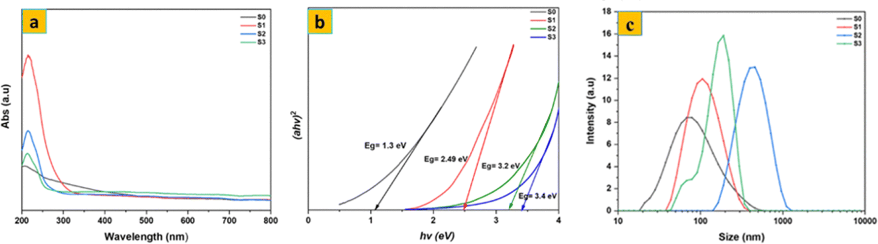 | ||
| Fig. 4 UV-vis spectra of (a) and (b) corresponding direct band gap of S0, S1, S2, and S3; (c) particle size distribution of S0, S1, S2 and S3 aqueous dispersions. | ||
Fig. 4c shows the particle size distribution of the synthesized S0 and MoO3 aqueous samples. The S0 nanosheets have a smaller average particle size (71 nm) compared to the MoO3 samples: 103 nm for S1, 413 nm for S2, and 191 nm for S3. This size difference is mainly due to the distinct crystal structures and atomic coordination geometries. MoS2 has a layered structure in which each Mo atom is bonded to two S atoms in a trigonal prismatic geometry, with the layers held together by weak van der Waals forces. This layered arrangement results in smaller particle size. From Fig. S1, the zeta potential peak of the synthesized S0 is found at −40.3 mV, while the MoO3 samples (S1, S2, S3) have peaks at −51.1 mV, −42 mV, and −46.1 mV at pH = 7, indicating that both S0 and MoO3 samples carry a negative surface charge.36
The functional groups of the prepared samples were examined by ATR-IR spectroscopy (Fig. S2). The ATR-IR spectrum of S0 shows distinct peaks at 639 cm−1, 896.39 cm−1, 1402.99 cm−1, and 1622.8 cm−1, which are characteristic of MoS2. The 3183.23 cm−1 peak is associated with an S–S bond, while the 931.39 cm−1 peak corresponds to another S–S bond. The presence of peaks at 3182 cm−1 also indicates the O–H stretching vibration.37 MoO3 samples show significant peaks below 1000 cm−1, notably at 981 cm−1, corresponding to the terminal MoO double bond and layered α-MoO3. The peak at 861 cm−1 is assigned to Mo–O–Mo bending vibrational modes, while the 560 cm−1 peak corresponds to Mo–O–Mo stretching modes. Additionally, the peak at 473 cm−1 is attributed to the terminal Mo–O bond stretching vibration.38
The BET surface areas of the synthesized samples were evaluated by nitrogen adsorption–desorption isotherm measurements (Fig. 5). Summarizes the results of N2 sorption measurements. The obtained BET surface areas for S0, S1, S2, and S3 were found to be 10.44, 14.39, 3.23, and 12.34 m2 g−1, respectively (Table S1). Among the MoO3 samples, S1 shows the highest surface area due to its thin nanoflake morphology, while S2 has the lowest due to its dense nanoplate structure. S3, with its fiber-like morphology, shows an intermediate surface area. The pore size distribution curves indicate that all samples possess mesoporous structures, with pore sizes ranging between 2 and 50 nm.39,40
 | ||
| Fig. 5 N2 sorption isotherms of synthesized S0, S1, S2, and S3. | ||
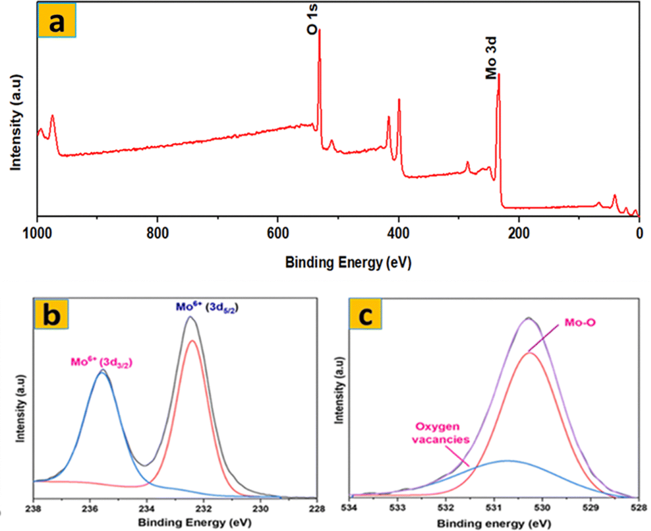
The surface elemental composition and chemical states of the synthesized samples were examined by XPS analysis. The XPS survey spectrum of S1 (Fig. 6a) confirms the presence of Mo and O as the main elements, without any detectable impurities. The high-resolution Mo 3d XPS spectrum (Fig. 6b) revealed two robust peaks associated with Mo6+. The doublet at 235.53 and 232.38 eV corresponds to Mo 3d3/2 and Mo 3d5/2 of Mo6+, respectively. Additionally, the core-level O 1s spectrum was deconvoluted into three peaks (529.90, 530.48, and 531.5 eV) as illustrated in Fig. 6c. Lattice O is responsible for the 529.90 eV peak, Mo–O for the 530.48 eV peak, and oxygen vacancies in S1 for the 531.5 eV peak. These XPS results confirm the successful transformation of MoS2 into phase-pure α-MoO3 after thermal annealing, as no sulfur-related peaks are detected in S1.
 | ||
| Fig. 6 XPS spectra of S1: (a) survey spectrum; (b) Mo 3d; (c) O 1s. | ||
The TEM image in Fig. 7a illustrates the bulk of α-MoO3 nanoflakes (S1) have a quadrilateral flask-like structure, with dimensions of around 1000 nm × 600 nm. The thickness of these nanoflakes is exceedingly thin, measuring just a few nanometers, which is aligned with the FE-SEM micrographs shown in Fig. 1d–f. Fig. 7(a) and (b) show HRTEM images of the edge of an α-MoO3 nanoflakes. The image shows two-dimensional lattice stripes, indicating that the α-MoO3 nanoflakes is a single crystal. Furthermore, in Fig. 3d, the lattice spacing of around 0.2 nm corresponds to the (002) crystalline planes of MoO3. Fig. 8 shows that the components Mo and O are evenly distributed throughout the MoO3 nanoflakes. This demonstrates the successful calcination of 70% 1T/2H MoS2 at 400 °C. The atomic percentages of oxygen and molybdenum were calculated using EDS data to be 76.1% 0.202 and 23.91% 0.202, respectively. As a result, the ratio of O to Mo atoms is three, yielding the typical chemical formula MoO3.
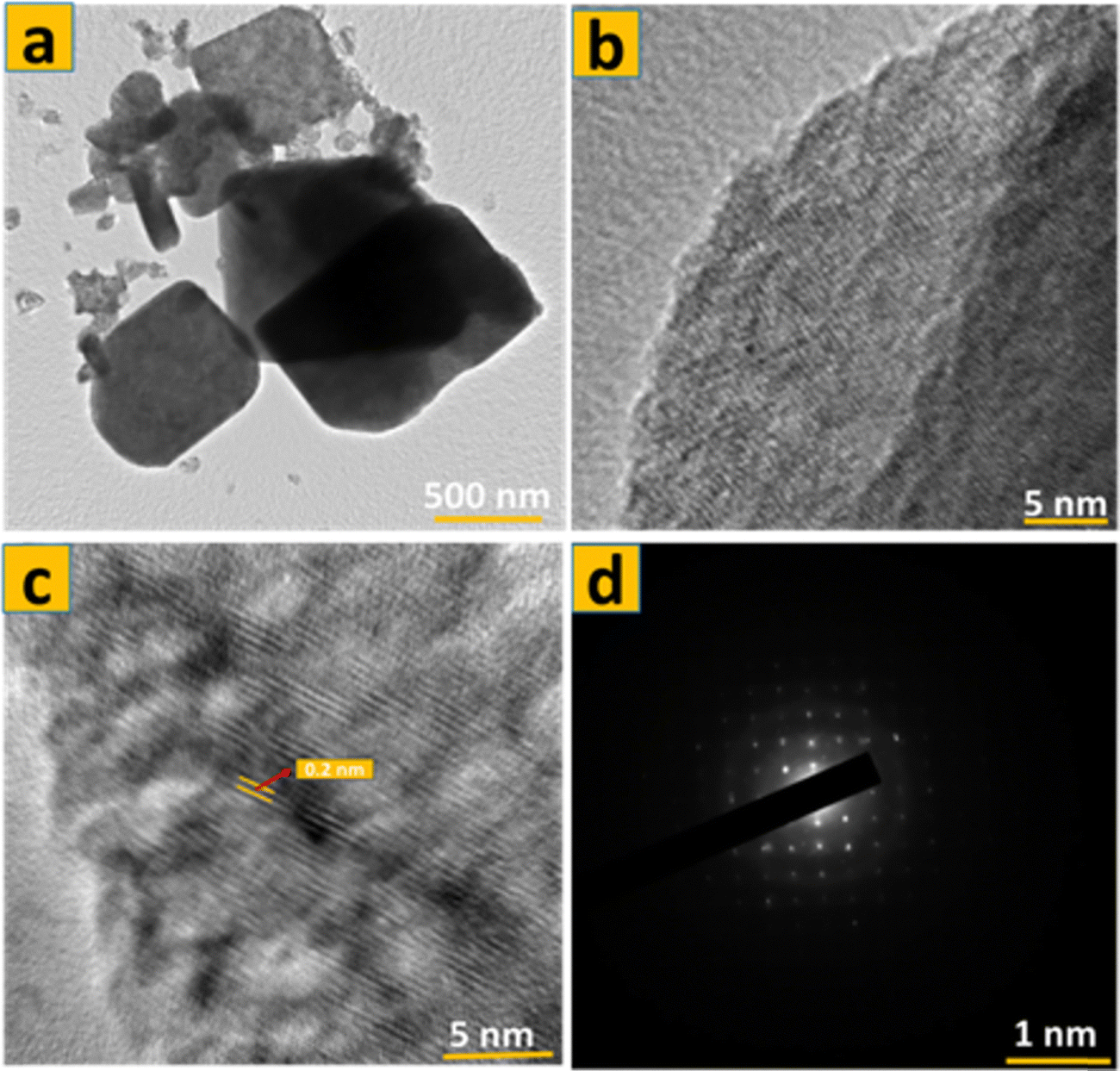 | ||
| Fig. 7 (a) TEM image of S1; (b) and (c) an HRTEM image of nanoflakes; (d) an SAED pattern. | ||
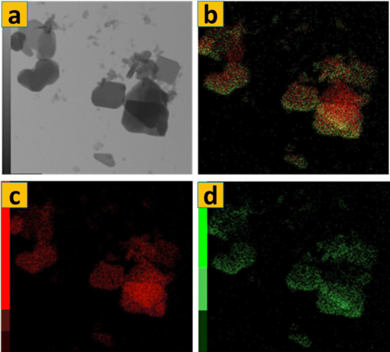 | ||
| Fig. 8 EDS mapping of S1. | ||
3.2. Electrochemical analysis
A comprehensive electrochemical characterization was conducted on a series of molybdenum-based nanostructures through cyclic voltammetry (CV). The investigation focused on hydrothermally synthesized 1T/2H-MoS2 nanosheets (S0) and the α-MoO3 nanoflakes (S1) derived from them via a meticulously controlled thermal annealing process. To establish a robust comparative framework, α-MoO3 nanoplates (S2), prepared through calcination, and nanofibers (S3), synthesized via a separate hydrothermal route, were also included. All electrodes were tested in 1 M H2SO4 within a potential range of 0–1 V at scan rates from 5 to 100 mV s−1, enabling a systematic evaluation of their kinetic behavior and charge-storage mechanisms. The CV profiles presented in Fig. 9(a)–(d) reveal distinct electrochemical responses: S0 displays quasi-rectangular curves, characteristic of capacitive surface-dominated processes, while S1–S3 exhibit well-defined redox peaks corresponding to reversible proton intercalation (MoO3 + xH+ + xe− ⇄ HxMoO3). Notably, S1 demonstrates the highest peak currents with minimal polarization, signifying superior capacitance and fast charge-transfer kinetics. This outstanding performance is attributed to its novel flake-like morphology, which provides abundant edge sites, high surface area, and short ion diffusion lengths, while controlled annealing introduces oxygen vacancies and mixed-valence Mo centers that enhance conductivity and redox activity. Such a synergistic structure-defect interplay is rarely achieved in conventional MoO3 electrodes and marks a clear novelty of this work. For instance, Saifullah et al. reported ∼671 F g−1 for hierarchical MoO3/CdO composites, but their bulkier nanobelt–particle morphology limited ion accessibility compared to the defect-rich flakes observed here.41 Similarly, recent studies demonstrated that microstructural optimization and oxygen vacancy engineering are essential to maximize α-MoO3 performance in acidic electrolytes.42 Compared to S2 and S3, which suffer from less favorable morphologies that restrict charge mobility and ion transport, S1 emerges as a structurally and functionally optimized electrode. Thus, the integrated electrochemical analysis not only underscores the superior performance of S1 but also establishes a novel synthesis–structure–property relationship, positioning defect-engineered MoO3 nanoflakes as a promising candidate for next-generation energy storage applications.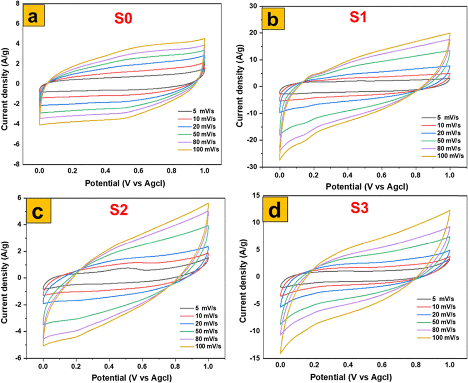 | ||
| Fig. 9 Electrochemical performances of MoS2 and MoO3 based electrodes in a three-electrode cell: CV of (a) MoS2, (b) MoO3 (S1), (c) MoO3 (S2), and MoO3 (S3). | ||
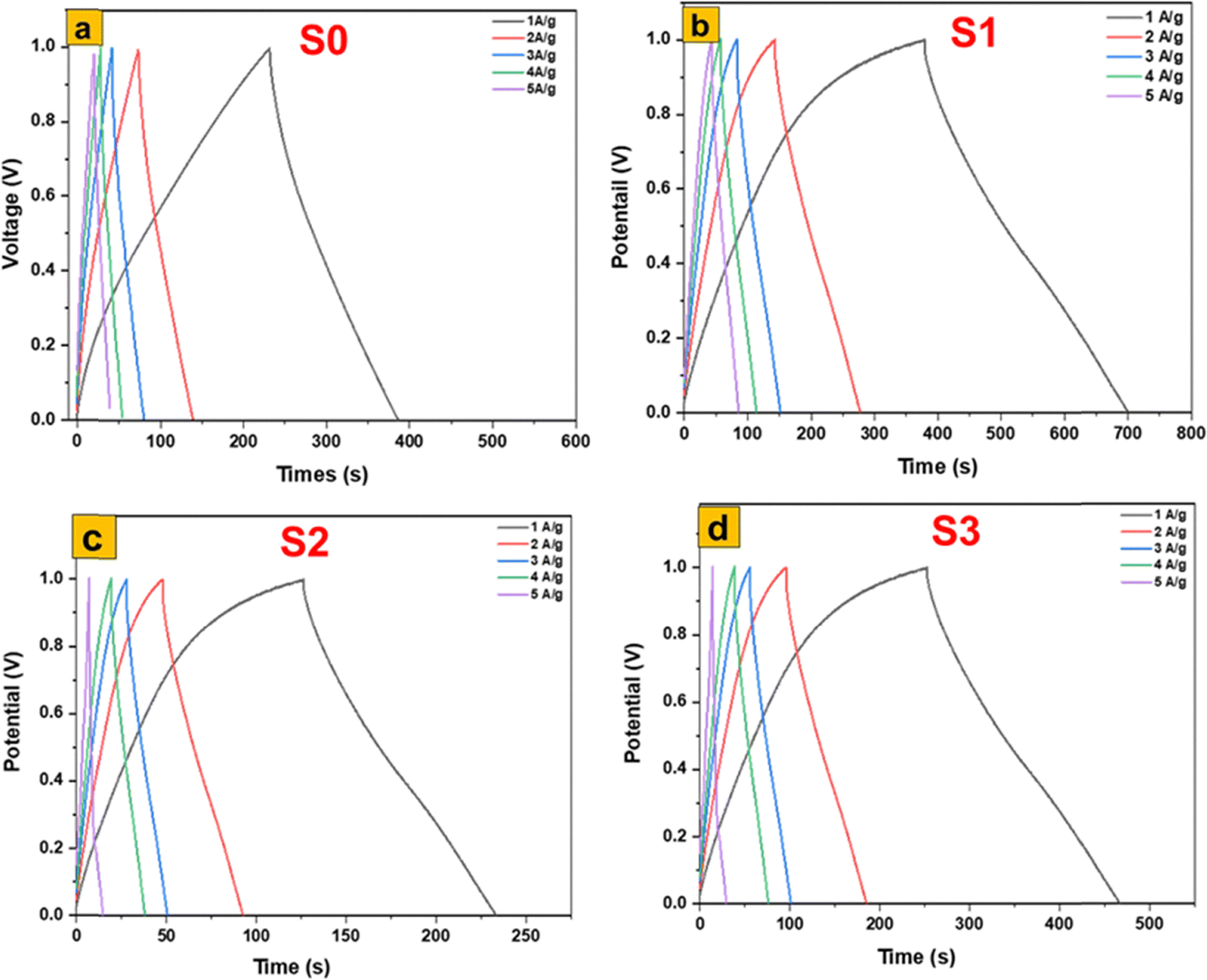
The galvanostatic charge–discharge (GCD) analysis presented in Fig. 10 clearly demonstrates the profound impact of synthesis method and resulting morphology on the electrochemical behavior of MoS2- and MoO3-based electrodes. Among the four investigated samples, the α-MoO3 nanoflakes obtained from the thermal annealing of 1T/2H-MoS2 nanosheets (S1) exhibit the highest electrochemical performance, delivering the longest discharge times, which directly reflect superior specific capacitance and energy storage capability. This outstanding behavior can be attributed to the unique two-dimensional flake-like architecture of S1, which combines a high surface-to-volume ratio with short diffusion paths for proton transport, while the moderate crystallinity introduced by annealing improves electrical conductivity without eliminating structural defects that act as active sites. The interconnected nanoflake domains thus create a synergistic balance between ion accessibility and electron mobility, leading to fast redox reactions and high charge-storage efficiency. In contrast, the hydrothermally synthesized α-MoO3 nanofibers (S3) also display remarkable performance, ranking second, owing to their one-dimensional architecture, which promotes continuous ion/electron pathways and large accessible surface areas; however, the relatively thicker fiber diameters compared to the ultrathin flakes result in longer transport distances and partial diffusion limitations that slightly reduce capacitance relative to S1. The calcined α-MoO3 nanoplates (S2) achieve a more moderate electrochemical activity: while improved crystallinity from calcination enhances conductivity and stability, the dense and relatively stacked plate-like morphology lowers porosity and restricts electrolyte penetration, leading to inferior capacitance compared to S1 and S3. Finally, the flower-like 1T/2H-MoS2 nanosheets (S0) perform the weakest, which can be linked to the coexistence of semiconducting 2H and metallic 1T phases where restacking diminishes effective surface exposure, thereby limiting pseudocapacitive activity despite the inherent conductivity of the 1T phase. These trends strongly emphasize the morphological–electrochemical relationship, which has also been confirmed in recent reports. For instance, Roy et al.43 demonstrated that tailoring MoO3 morphology in MoO3/CdO heterostructures significantly enhanced capacitance (671 F g−1) and reduced charge-transfer resistance, highlighting the role of structural engineering in boosting supercapacitor efficiency. Likewise, Ponelakkia et al. (2025)44 reported that transition-metal-doped MoO3 nanorods exhibit enhanced pseudocapacitive behavior with improved charge transfer and active-site availability. Their study showed that Ni-doped MoO3 nanorods can achieve a high specific capacitance of 167.95 F g−1 at 0.5 A g−1 with 99.79% retention over 15000 cycles, demonstrating excellent electrochemical stability. In addition, optimized MoO3 nanorods synthesized in 2024 were reported to reach ∼244 F g−1 with excellent cycling stability,45 again underscoring the positive influence of high-surface-area, defect-rich morphologies in supporting pseudocapacitive activity. Comparative studies on MoS2 electrodes further corroborate our observations: while MoS2 nanosheets can offer moderate capacitive contributions, they are often surpassed by oxide-based systems such as MoO3 due to the latter's richer redox chemistry and higher intrinsic pseudocapacitance.46 Collectively, the present findings and the cited works reinforce the principle that nanostructural control—especially ultrathin 2D nanoflakes as in S1—remains the most decisive factor in optimizing the electrochemical storage properties of MoO3, since they simultaneously maximize the density of active sites, minimize transport barriers, and balance crystallinity with defect-driven reactivity. These insights strongly suggest that the development of next-generation MoO3-based electrodes should prioritize flake- and fiber-type morphologies over denser plate-like or aggregated structures to achieve practical, high-performance supercapacitor devices.
 | ||
| Fig. 10 Electrochemical performances of MoS2 and MoO3 based electrodes in a three-electrode cell: GCD of (a) MoS2, (b) MoO3 (S1), (c) MoO3 (S2), and MoO3 (S3). | ||
Fig. 11a–d provide a detailed comparison of the electrochemical performance of MoS2 nanosheets and three distinct MoO3 morphologies: thermally annealed MoO3 nanoflakes, MoO3 fibers, and MoO3 nanoplates. The cyclic voltammetry (CV) curves at 5 mV s−1 (Fig. 11a) clearly show that the thermally annealed MoO3 nanoflakes exhibit the largest integrated area, corresponding to the highest specific capacitance of 755 F g−1. This superior performance reflects their optimized balance of accessible redox sites, ion diffusion pathways, and electrical conductivity. In contrast, MoO3 fibers occupy a strong second position, delivering 455 F g−1, as their elongated structure facilitates relatively efficient charge transport but provides fewer surface-active sites compared to the nanoflakes. MoO3 nanoplates show much lower capacitance (175 F g−1), penalized by diffusion and porosity limitations that restrict ion accessibility. Finally, MoS2 nanosheets deliver a moderate specific capacitance of 250 F g−1, reflecting their layered architecture that supports pseudocapacitive charge storage but is intrinsically constrained by slower ion intercalation kinetics.
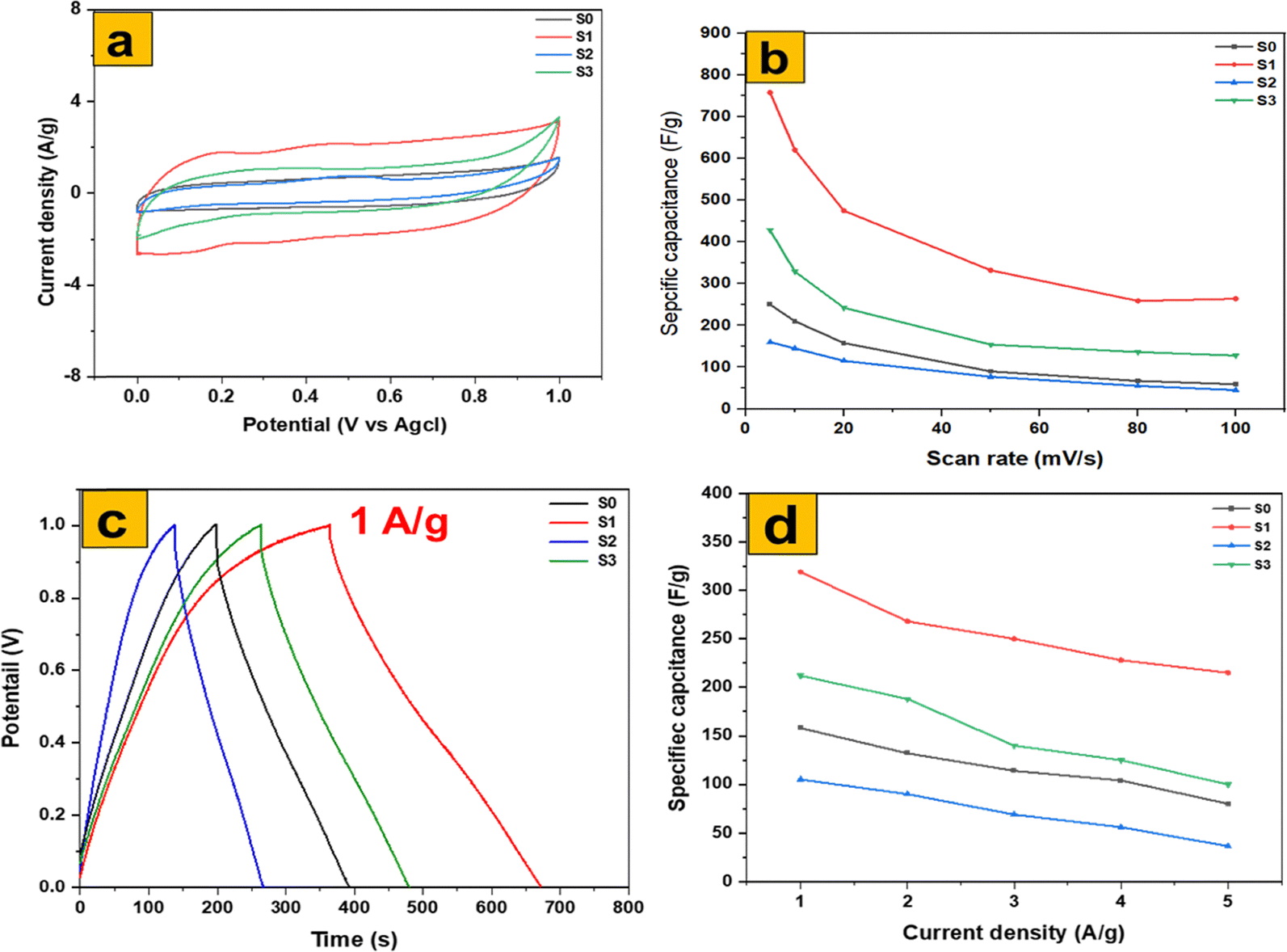 | ||
| Fig. 11 Electrochemical comparison of MoS2 and MoO3 for (a) CV at 5 mV s−1, (b) GCD at 1 A g−1, (c) CV-specific capacitance, and (d) GCD-specific capacitance. | ||
Galvanostatic charge–discharge (GCD) curves at 1 A g−1 (Fig. 11c) further reinforce these observations. The MoO3 nanoflakes again show the longest discharge time (325 F g−1), highlighting their ability to sustain higher charge storage. MoO3 fibers (230 F g−1) follow, while MoS2 nanosheets (145 F g−1) provide intermediate performance, and MoO3 nanoplates remain the poorest performer (105 F g−1). The rate-capability plots (Fig. 11b and d) confirm these trends, as MoO3 nanoflakes maintain a high capacitance retention even under fast charge–discharge conditions, whereas the nanoplates suffer from rapid performance decay.
Overall, thermally annealed MoO3 nanoflakes optimize the balance of accessible redox-active sites, ion pathways, and conductivity to deliver the best performance. MoO3 fibers provide a strong kinetic second due to their elongated channels, MoO3 nanoplates are penalized by diffusion and porosity limitations, and MoS2 nanosheets remain constrained by intrinsically weaker charge transport and ion storage properties. These results are fully consistent with recent reports emphasizing the morphology–performance relationship in MoO3 and MoS2-based electrodes.47,48
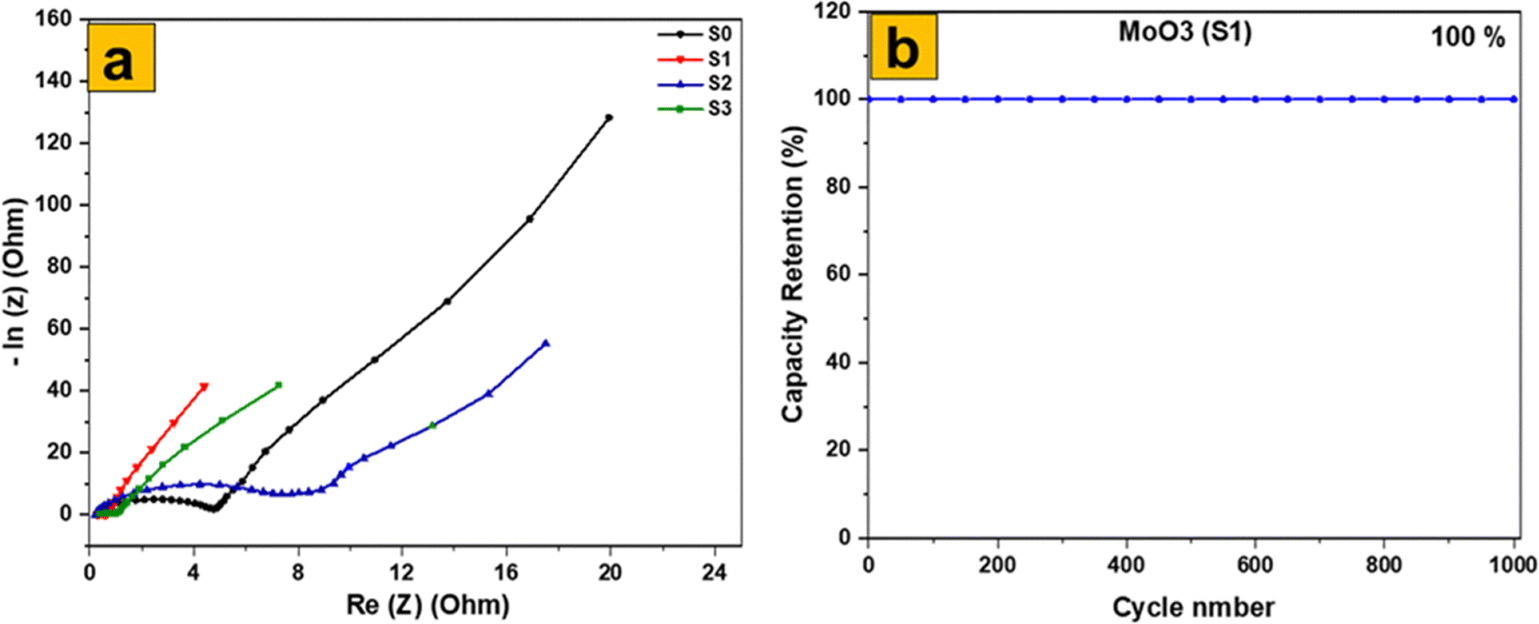
The electrochemical impedance spectroscopy (EIS) results for the four samples (Fig. 12a) reveal precise information on their electrochemical characteristics, with an emphasis on charge transfer resistance (Rct) and equivalent series resistance (RESR). The MoS2 sample, with a Rct of 0.34 Ω and RESR of 4.6 Ω, has a modest charge transfer efficiency but greater internal resistance, which affects its conductivity. Among the MoO3 samples, the MoO3-S1 stands out with the lowest Rct (0.14 Ω) and RESR (0.7 Ω), indicating highly efficient charge transfer and minimal internal resistance, making it the most promising for energy storage applications. The MoO3-S2 shows higher values with an Rct of 0.39 Ω and RESR of 7.6 Ω, suggesting less effective charge transfer and higher internal resistance. The hydrothermal MoO3-S3 has intermediate performance with an Rct of 0.21 Ω and RESR of 1.18 Ω, reflecting a balance between charge transfer capability and internal resistance. These findings underscore the critical influence of preparation methods and morphologies on the electrochemical performance of MoS2 and MoO3, with the thermally calcined MoO3 exhibiting the best properties, followed by the hydrothermal and precipitated MoO3 samples. Understanding these variations helps in optimizing the materials for advanced energy storage applications. Additionally, Fig. 12b shows that the MoO3 (S1) electrode has a trustworthy life cycle, with an amazing capacity retention rate of 100% after 1000 cycles of cyclic stability testing. This highlights the excellent durability and long-term performance of the MoO3 electrode, making it highly suitable for practical energy storage applications. The electrochemical performance of orthorhombic MoO3 with 2D nanoflakes was compared to other literature in Table 1.
 | ||
| Fig. 12 (a) EIS comparison and (b) capacity retention of S1. | ||
3.2. Two-electrode electrochemical analysis of MoO3-S1
To assess the practical device-level performance, a symmetric supercapacitor (MoO3-S1//MoO3-S1) was fabricated and tested using a two-electrode configuration. The cyclic voltammetry (CV) curves recorded at scan rates from 5 to 100 mV s−1 (Fig. 13a) indicate dominant capacitive behavior, with a gradual decrease in current response at higher scan rates due to kinetic limitations in ion transport. The specific capacitance calculated from CV reached 382 F g−1 at 5 mV s−1, demonstrating excellent charge storage capability under slow scan conditions. Galvanostatic charge–discharge (GCD) measurements at current densities from 1 to 5 A g−1 (Fig. 13c) show nearly linear charge–discharge profiles, indicative of stable capacitive behavior. The maximum specific capacitance of 206 F g−1 at 1 A g−1 gradually decreases at higher current densities due to limited ion diffusion and internal resistance effects. The Ragone plot for MoO3-S1 (Fig. S4) further demonstrates a power density of 512 W kg−1 and an energy density of 28.47 Wh kg−1 at a current density of 1 A g−1. Even at a higher current density of 5 A g−1, the MoO3-S1 supercapacitor maintains an energy density of 14.17 Wh kg−1. These results confirm that MoO3-S1 exhibits high capacitance, good rate capability, and competitive energy–power performance in a practical two-electrode configuration, highlighting its potential for supercapacitor applications.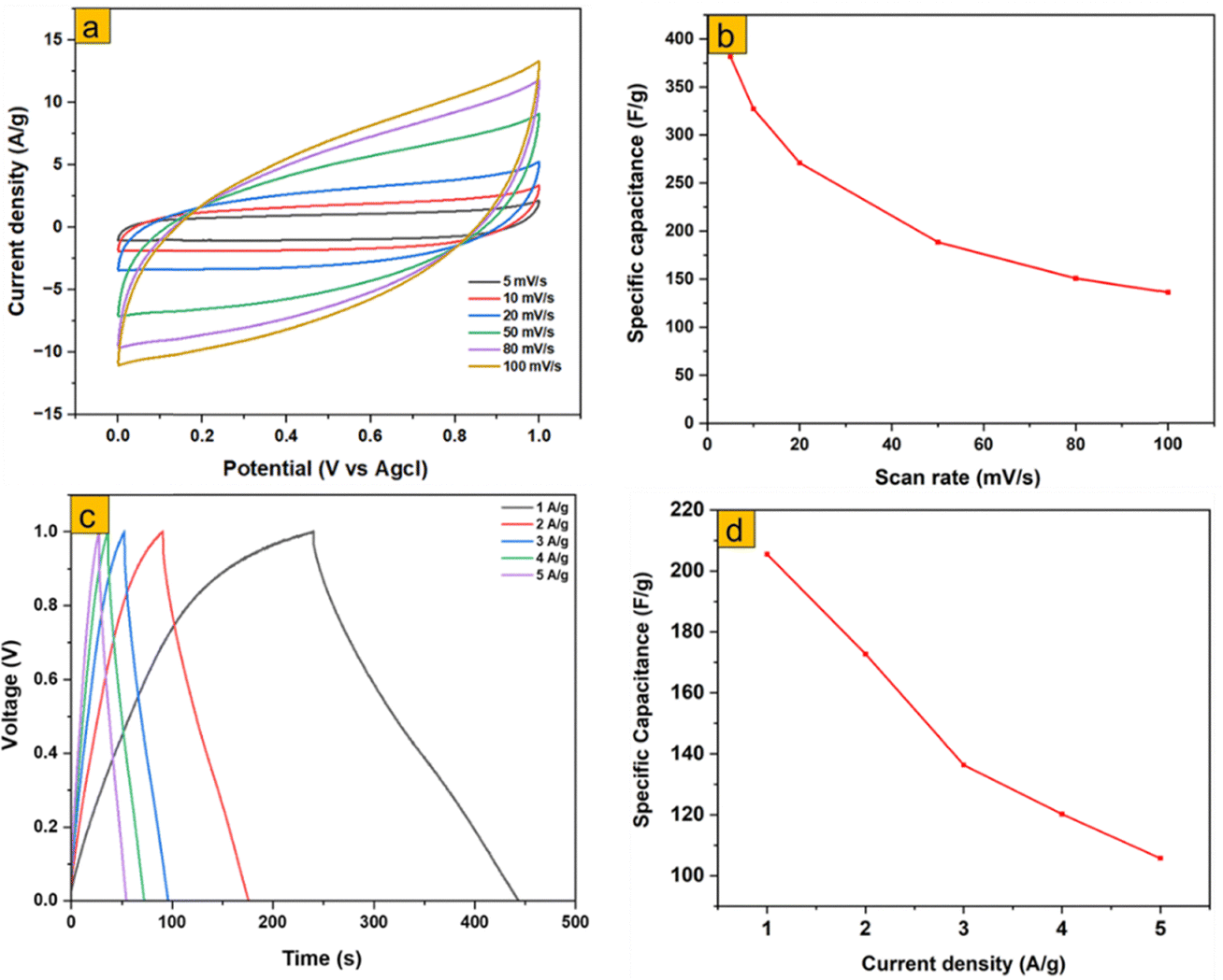 | ||
| Fig. 13 Two-electrode electrochemical performances; (a) CV plots, (b) CV specific capacitance, (c) GCD plots, and (c) GCD plots, and (d) GCD-specific capacitance of MoO3-S1//MoO3-S1. | ||
3.3. Charge storage mechanism
Scheme 2 illustrates the proposed charge-storage mechanism for the Mo-based electrodes in 1 M H2SO4. In S1 (thermally annealed MoO3 nanoflakes), the porous, interconnected architecture facilitates rapid diffusion of protons and redox-active species, which initially occupy confined states before transitioning to adsorbed or surface redox-active states where electron transfer occurs. The high density of oxygen vacancies further enhances electrokinetics by improving electronic conductivity, accelerating proton insertion/extraction, and providing additional active sites that strengthen surface redox reactions, resulting in the highest capacitance (755 F g−1 from CV, 325 F g−1 from GCD), in agreement with previous reports highlighting the benefits of defect-rich, porous morphologies for supercapacitor performance.58,59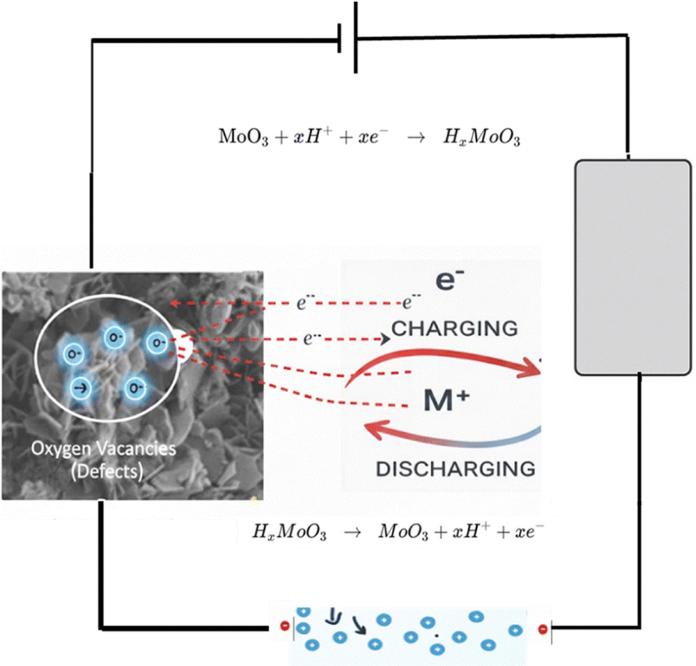 | ||
| Scheme 2 Schematic illustration of the proposed mechanism of electrochemical interactions. | ||
S2 (MoO3 fibers) shows moderate capacitance (455 F g−1 CV, 230 F g−1 GCD); although the elongated fiber morphology provides relatively efficient ion and electron pathways, the lower defect density and fewer accessible redox sites limit both surface-controlled and diffusion-controlled kinetics, consistent with prior observations on morphology-dependent charge storage (Liu et al., 2024). S3 (MoS2 nanosheets) stores charge primarily via proton intercalation into the S–Mo–S layers (MoS2 + xH+ + xe− ↔ HxMoS2). However, reduced intrinsic conductivity and slower proton transport result in moderate capacitance (250 F g−1 CV, 145 F g−1 GCD), highlighting the critical role of intrinsic electronic properties and ion-transport kinetics.60 S4 (MoO3 nanoplates) exhibits the lowest capacitance (175 F g−1 CV, 105 F g−1 GCD) due to compact morphology, which restricts ion access, limits interfacial contact, and slows both ionic and electronic transport, in line with previous studies emphasizing the importance of accessible surface area and porosity for fast charge storage (Simsek et al., 2026).
Overall, the trend S1 > S2 > S3 > S4 highlights that electrode morphology, oxygen-vacancy-driven defect chemistry, and the density of accessible redox sites collectively govern capacitive behavior and charge-transfer kinetics. Fast electrokinetic processes—such as surface redox reactions, confined-state transitions, and rapid proton migration—are most effectively promoted in the highly porous, defect-rich S1 electrode, corroborating literature reports on the critical influence of structural porosity, defect engineering, and morphology optimization on supercapacitor performance.61
4. Conclusions
Thermal annealing of hydrothermally developed 1T/2H MoS2 results in a novel nanoflakes-like structure of α-MoO3. The flower-like MoS2 sample was synthesized at 200 °C and annealed at 400 °C for 30 minutes. After annealing at 400 °C, the sample converted into orthorhombic MoO3 with 2D plates. The formation of the hybrid nanostructure and the temperature progression of MoS2 have been confirmed by XRD, Raman, FESEM, EDX, BET, and XPS. The increased surface area of the nanoflakes-like structure is due to the presence of interstitial and lattice oxygen species. The samples' electrochemical performance was tested using cyclic voltammetry, galvanostatic charging–discharging, and electrochemical impedance analysis, with considerably improved findings compared to earlier α-MoO3-based research. The electrochemical performance of an α-MoO3 nanoparticles as the active electrode material was fully examined. The supercapacitor performance of the samples was compared in 1 M H2SO4 with a mass loading of 1 mg. The flakes-like structure had a specific conductance of 325 F g−1, which was twice as high as the other structures.Conflicts of interest
There are no conflicts to declare.Data availability
Upon reasonable request, raw data regarding this work can be requested from the corresponding author.The data supporting this article have been included as part of the supplementary information (SI). Supplementary information is available. See DOI: https://doi.org/10.1039/d5ma01084e.
Acknowledgements
The authors gratefully thank the financial support provided of DAAD from the fund of BMZ through the We-AFRICA project No. 57708984. We are also grateful for the additional support provided by AfriGer-SDG DAAD project.References
- A. M. Çolak and E. Irmak, Electric Vehicle Advancements, Barriers, and Potential: A Comprehensive Review, Electr. Power Compon. Syst., 2023, 51(17), 2010–2042, DOI:10.1080/15325008.2023.2239238.
- Md. Y. Bhat, S. A. Hashmi, M. Khan, D. Choi and A. Qurashi, Frontiers and recent developments on supercapacitor's materials, design, and applications: Transport and power system applications, J Energy Storage, 2023, 58(17), 106104, DOI:10.1016/j.est.2022.106104.
- S. Shin, J. W. Gittins, C. J. Balhatchet, A. Walsh and A. C. Forse, Metal–Organic Framework Supercapacitors: Challenges and Opportunities, Adv. Funct. Mater., 2024, 34, 43, DOI:10.1002/adfm.202308497.
- M. Girirajan, A. K. Bojarajan, I. N. Pulidindi, K. N. Hui and S. Sangaraju, An insight into the nanoarchitecture of electrode materials on the performance of supercapacitors, Coord. Chem. Rev., 2024, 518, 216080, DOI:10.1016/j.ccr.2024.216080.
- S. R. E. Mohamed, M. R. R. Abdul-Aziz, S. Saber, G. Khabiri and A. S. G. Khalil, Precise engineering of Fe3O4/MWCNTs heterostructures for high-performance supercapacitors, J. Alloys Compd., 2023, 957, 170281, DOI:10.1016/j.jallcom.2023.170281.
- S. R. Mohamed, A. S. Mohammed, O. I. Metwalli, S. El-Sayed, G. Khabiri, A. Hassan and A. S. Khalil, Synergistic design of high-performance symmetric supercapacitor based on iron oxide nanoplatelets/COOH-MWCNTs heterostructures: DFT computation and experimental analysis, J. Alloys Compd., 2024, 987, 174118 CrossRef CAS.
- Ö. Taş, Z. Kudaş and D. Ekinci, Electrochemical performance of diazonium-generated carbon films for electrochemical double-layer capacitors (EDLCs), Diam. Relat. Mater., 2023, 138, 110227, DOI:10.1016/j.diamond.2023.110227.
- S. Mahala, K. Khosravinia and A. Kiani, Unwanted degradation in pseudocapacitors: Challenges and opportunities, J. Energy Storage, 2023, 67, 107558, DOI:10.1016/j.est.2023.107558.
- L. Yao, et al., Structural pseudocapacitors with reinforced interfaces to increase multifunctional efficiency, Sci. Adv., 2023, 9(25) DOI:10.1126/sciadv.adh0069.
- S. Katwesigye, M. E. El-Khouly, N. López-Salas and A. S. Khalil, Value-added utilization of biowaste-derived lignin towards the synthesis of oxygen-enriched hierarchical laser-induced graphene and its application as a micro-supercapacitor, J. Energy Storage, 2025, 105, 114752 CrossRef.
- M. Rajapakse, et al., Intercalation as a versatile tool for fabrication, property tuning, and phase transitions in 2D materials, NPJ 2D Mater. Appl., 2021, 5(1), 30, DOI:10.1038/s41699-021-00211-6.
- A. Hayat, et al., Recent advances, properties, fabrication and opportunities in two-dimensional materials for their potential sustainable applications, Energy Storage Mater., 2023, 59, 102780, DOI:10.1016/j.ensm.2023.102780.
- Z. Kuspanov, B. Bakbolat, A. Baimenov, A. Issadykov, M. Yeleuov and C. Daulbayev, Photocatalysts for a sustainable future: Innovations in large-scale environmental and energy applications, Sci. Total Environ., 2023, 885, 163914, DOI:10.1016/j.scitotenv.2023.163914.
- B. B. Sahoo, et al., A state-of-art review on 2D material-boosted metal oxide nanoparticle electrodes: Supercapacitor applications, J. Energy Storage, 2023, 65, 107335, DOI:10.1016/j.est.2023.107335.
- R. Kumar, S. Sahoo, E. Joanni, R. K. Singh and R. M. Yadav, Graphene-metal oxide hybrid materials with 2D and 3D morphologies for advanced supercapacitor electrodes: Status, challenges and prospects, Mater. Today Nano, 2023, 24, 100399, DOI:10.1016/j.mtnano.2023.100399.
- A. S. Adekunle, et al., Potential of cobalt and cobalt oxide nanoparticles as nanocatalyst towards dyes degradation in wastewater, Nano-Struct. Nano-Objects, 2020, 21, 100405, DOI:10.1016/j.nanoso.2019.100405.
- M. Luo, J. Yang, X. Li, M. Eguchi, Y. Yamauchi and Z.-L. Wang, Insights into alloy/oxide or hydroxide interfaces in Ni–Mo-based electrocatalysts for hydrogen evolution under alkaline conditions, Chem. Sci., 2023, 14(13), 3400–3414, 10.1039/D2SC06298D.
- H. H. Ali, et al., Rationally designed Mo-based advanced nanostructured materials for energy storage technologies: Advances and prospects, Sustainable Mater. Technol., 2023, 38, e00738, DOI:10.1016/j.susmat.2023.e00738.
- H. Gupta, S. Chakrabarti, S. Mothkuri, B. Padya, T. N. Rao and K. Jain, High performance supercapacitor based on 2D-MoS2 nanostructures, Mater. Today Proc., 2020, 26, 20–24, DOI:10.1016/j.matpr.2019.04.198.
- K. K. Patel, T. Singhal, V. Pandey, T. Sumangala and M. S. Sreekanth, Evolution and recent developments of high performance electrode material for supercapacitors: A review, J. Energy Storage, 2021, 44, 103366, DOI:10.1016/j.est.2021.103366.
- B. Li, et al., Inkjet-Printed Ultrathin MoS2-Based Electrodes for Flexible In-Plane Microsupercapacitors, ACS Appl. Mater. Interfaces, 2020, 12(35), 39444–39454, DOI:10.1021/acsami.0c11788.
- X. Geng, et al., Two-Dimensional Water-Coupled Metallic MoS2 with Nanochannels for Ultrafast Supercapacitors, Nano Lett., 2017, 17(3), 1825–1832, DOI:10.1021/acs.nanolett.6b05134.
- S. A. Mensah, A. M. F. El-Bab, Y. Tominaga and A. S. Khalil, Precisely engineered interface of laser-induced graphene and MoS2 nanosheets for enhanced supercapacitor electrode performance, Appl. Surf. Sci., 2025, 688, 162230 CrossRef CAS.
- D. Zhao, et al., Facile synthesis of MoO3 nanospheres and their application in water treatment, Mater. Lett., 2019, 256, 126648, DOI:10.1016/j.matlet.2019.126648.
- S. Jamil, G. Zahra and M. R. S. A. Janjua, Morphologically controlled synthesis, characterization, and applications of molybdenum oxide (MoO3) nanoparticles, J. Phys. Org. Chem., 2023, 36(4) DOI:10.1002/poc.4477.
- B. Yao, et al., Flexible Transparent Molybdenum Trioxide Nanopaper for Energy Storage, Adv. Mater., 2016, 28(30), 6353–6358, DOI:10.1002/adma.201600529.
- J. Gong, et al., Vanadate ion promoting the transformation of α-phase molybdenum trioxide (α-MoO3) to h-phase MoO3 (h-MoO3) for boosted Zn-ion storage, J. Colloid Interface Sci., 2023, 647, 115–123, DOI:10.1016/j.jcis.2023.05.146.
- C. Cheng, A. Wang, M. Humayun and C. Wang, Recent advances of oxygen vacancies in MoO3: preparation and roles, Chem. Eng. J., 2024, 498, 155246, DOI:10.1016/j.cej.2024.155246.
- A. Raza, M. Ali, N. Ayub, S. Atta and M. Jawad, Chemical vapor deposition-based synthesis of binder-free nanostructure α-MoO 3 electrode material for PES devices, Phys. Scr., 2024, 99(5), 055910, DOI:10.1088/1402-4896/ad3502.
- T. S. Sian and G. B. Reddy, Optical, structural and photoelectron spectroscopic studies on amorphous and crystalline molybdenum oxide thin films, Solar Energy Mater. Solar Cells, 2004, 82(3), 375–386, DOI:10.1016/j.solmat.2003.12.007.
- R. B. Pujari, V. C. Lokhande, V. S. Kumbhar, N. R. Chodankar and C. D. Lokhande, Hexagonal microrods architectured MoO3 thin film for supercapacitor application, J. Mater. Sci.: Mater. Electron., 2016, 27(4), 3312–3317, DOI:10.1007/s10854-015-4160-3.
- S. S. Pradeepa, K. Sutharthani, R. Suba Devi, W.-R. Liu and M. Sivakumar, Investigation on two-dimensional molybdenum oxide-graphitic carbon nitride (MoO3-g-C3N4) heterostructures based hybrid electrodes for the fabrication of high energy density solid state supercapacitors, J. Taiwan Inst. Chem. Eng., 2024, 154, 105084, DOI:10.1016/j.jtice.2023.105084.
- K. Krishnamoorthy, M. Premanathan, M. Veerapandian and S. Jae Kim, Nanostructured molybdenum oxide-based antibacterial paint: effective growth inhibition of various pathogenic bacteria, Nanotechnology, 2014, 25(31), 315101, DOI:10.1088/0957-4484/25/31/315101.
- J. Xu, L. Wang and Y. Zhu, Decontamination of Bisphenol A from Aqueous Solution by Graphene Adsorption, Langmuir, 2012, 28(22), 8418–8425, DOI:10.1021/la301476p.
- P.-P. Wang, H. Sun, Y. Ji, W. Li and X. Wang, Three-Dimensional Assembly of Single-Layered MoS2, Adv. Mater., 2014, 26(6), 964–969, DOI:10.1002/adma.201304120.
- P. Nagaraju, M. Arivanandhan, A. Alsalme, A. Alghamdi and R. Jayavel, Enhanced electrochemical performance of α-MoO3/graphene nanocomposites prepared by an in situ microwave irradiation technique for energy storage applications, RSC Adv., 2020, 10(38), 22836–22847, 10.1039/C9RA10873D.
- A. Ali, et al., Ultrathin MoS2 nanosheets for high-performance photoelectrochemical applications via plasmonic coupling with Au nanocrystals, Nanoscale, 2019, 11(16), 7813–7824, 10.1039/C8NR10320H.
- A. Manivel, et al., Synthesis of MoO3 nanoparticles for azo dye degradation by catalytic ozonation, Mater. Res. Bull., 2015, 62, 184–191, DOI:10.1016/j.materresbull.2014.11.016.
- Z. Kou, et al., A promising gene delivery system developed from PEGylated MoS2 nanosheets for gene therapy, Nanoscale Res. Lett., 2014, 9(1), 587, DOI:10.1186/1556-276X-9-587.
- K. C. Lalithambika, K. Shanmugapriya and S. Sriram, Photocatalytic activity of MoS2 nanoparticles: an experimental and DFT analysis, Appl. Phys. A, 2019, 125(12), 817, DOI:10.1007/s00339-019-3120-9.
- M. Saifullah, P. Roy, M. A. Zubair and M. R. Islam, Tuning the electrochemical performance of a hierarchical MoO3/CdO binary heterostructure for supercapacitor applications, Nanoscale Adv., 2025, 7, 5681–5700, 10.1039/D5NA00491H.
- P. Ondrejka, A. Petrík, M. Husár, Á. Straňovský, M. Kemény, M. Sojková, P. Novák and M. Mikolášek, Optimization of MoO3 microstructures through temperature control and KOH activation for improved supercapacitor electrode performance, Monatsh. Chem., 2025, 156(5), 1–6, DOI:10.1007/s00706-025-03318-4.
- S. Roy, A. Manna and S. Ghosh, Morphology-driven charge storage in MoO3/CdO heterostructures for high-performance supercapacitors, J. Energy Storage, 2025, 82, 111234, DOI:10.1016/j.est.2025.111234.
- D. K. Ponelakkia, K. Muhil Eswari, V. Balaji, P. Sakthivel, S. Asaithambi, R. Yuvakkumar and G. Ravi, Enhanced pseudocapacitive performance of transition metal doped MoO3 nanorods, Electrochim. Acta, 2025, 511, 145349, DOI:10.1016/j.electacta.2024.145349.
- X. Li, H. Zhao and Y. Chen, High-performance MoO3 nanorods for supercapacitor electrodes with improved cycling stability, J. Alloys Compd., 2024, 975, 172345, DOI:10.1016/j.jallcom.2024.172345.
- L. Zhao, A. Kumar and N. Singh, Comparative electrochemical performance of MoS2 and MoO3 nanostructures for energy storage applications, Appl. Surf. Sci., 2024, 635, 158059, DOI:10.1016/j.apsusc.2024.158059.
- Y. Chen, J. Wu and L. Wang, Hydrothermal engineering of MoO3 nanostructures for advanced electrochemical capacitors, Electrochim. Acta, 2024, 500, 142563, DOI:10.1016/j.electacta.2023.142563.
- D. R. Patel, M. Ghosh and A. K. Sharma, Electrochemical insights into MoS2/MoO3 heterostructures: synergistic charge storage for high-performance supercapacitors, Appl. Surf. Sci., 2024, 657, 159782, DOI:10.1016/j.apsusc.2023.159782.
- B. Liu, et al., Facile synthesis of oxygen-deficient MoO3−x nanosheets by light radiation for fast electrochromic supercapacitors, Electrochim. Acta, 2023, 464, 142894, DOI:10.1016/j.electacta.2023.142894.
- N. G. Prakash, M. Dhananjaya, A. L. Narayana, D. Shaik, P. Rosaiah and O. M. Hussain, High Performance One Dimensional α-MoO3 Nanorods for Supercapacitor Applications, Ceram. Int., 2018, 44(8), 9967–9975, DOI:10.1016/j.ceramint.2018.03.032.
- N. Palaniyandy, D. Lakshmi, G. Thenmozhi, S. Kheawhom and N. N. Musyoka, Enhanced electrochemical energy storage devices utilizing a one-dimensional (1D) α-MnO2 nanocomposite encased in onion-like carbon, J. Mater. Sci., 2024, 59(13), 5450–5469, DOI:10.1007/s10853-024-09373-2.
- K.-J. Huang, J.-Z. Zhang, G.-W. Shi and Y.-M. Liu, Hydrothermal synthesis of molybdenum disulfide nanosheets as supercapacitors electrode material, Electrochim. Acta, 2014, 132, 397–403, DOI:10.1016/j.electacta.2014.04.007.
- M. R. Charapale, et al., Hierarchical 3D flowers of 1T@2H-MoS2 assembled with an array of ultrathin nano-petals for high-performance supercapacitor electrodes, J. Solid State Electrochem., 2024, 28(1), 181–195, DOI:10.1007/s10008-023-05676-7.
- S. Muduli, S. K. Pati, S. Swain and S. K. Martha, MoO3@ZnO Nanocomposite as an Efficient Anode Material for Supercapacitors: A Cost Effective Synthesis Approach, Energy Fuels, 2021, 35(20), 16850–16859, DOI:10.1021/acs.energyfuels.1c01665.
- C. Zhou, et al., A facile route to synthesize Ag decorated MoO3 nanocomposite for symmetric supercapacitor, Ceram. Int., 2020, 46(10), 15385–15391, DOI:10.1016/j.ceramint.2020.03.083.
- K.-J. Huang, J.-Z. Zhang, G.-W. Shi and Y.-M. Liu, Hydrothermal synthesis of molybdenum disulfide nanosheets as supercapacitors electrode material, Electrochim. Acta, 2014, 132, 397–403, DOI:10.1016/j.electacta.2014.04.007.
- N. Shaheen, S. Zulfiqar, M. E. El Sayed, A. Samir, M. Shahid, M. F. Warsi and E. W. Cochran, Evaluation of energy storage mechanism and development of nanoarchitecture in 1D WS2/MoO3/MXene composite for supercapacitor applications, J. Alloys Compd., 2025, 1010, 178072, DOI:10.1016/j.jallcom.2024.178072.
- K.-J. Huang, J.-Z. Zhang, G.-W. Shi and Y.-M. Liu, Hydrothermal synthesis of molybdenum disulfide nanosheets as supercapacitors electrode material, Electrochim. Acta, 2014, 132, 397–403, DOI:10.1016/j.electacta.2014.04.00.
- G. Liu, L. Liu, G. Li, S. Wu, J. He, Y. Zhou, M. Demir and P. Ma, Temperature-dependent electrochemical performance of Ta-substituted SrCoO3 perovskite for supercapacitors, Chem. – Eur. J., 2024, 30(14), e202303267 CrossRef CAS PubMed.
- S. G. Colak, et al., Enhanced supercapacitor performance with CZTS-based carbon nanocomposites electrodes: An electrochemical study, J. Colloid Interface Sci., 2025, 682, 478–490 CrossRef CAS PubMed.
- A. K. Nayak, A. K. Das and D. Pradhan, High performance solid-state asymmetric supercapacitor using green synthesized graphene–WO3 nanowires nanocomposite, ACS Sustainable Chem. Eng., 2017, 5(11), 10128–10138 CrossRef CAS.
| This journal is © The Royal Society of Chemistry 2026 |