Stacking-switching of silicon-based two-dimensional diamane structures to enhance photocatalytic water splitting performance
Received
22nd October 2025
, Accepted 25th November 2025
First published on 28th November 2025
Abstract
Through first-principles calculations, we design and screen a series of Janus silicon-based two-dimensional (2D) diamane Si4HX (X = F, Cl and Br) structures as promising piezoelectric photocatalysts for water splitting. The transitions from the initial to the final states of the Si4HX monolayers lead to enhanced physical properties that characterize their photocatalytic performances. Notably, the reversal and enhancement of the intrinsic in-plane polarizations more efficiently drive in-plane carrier migrations, thereby enhancing carrier mobility. Furthermore, the extensive out-of-plane built-in electric fields combined with excellent piezoelectricity of the Si4HX monolayers further generate the strain-enhanced intrinsic electric fields, which effectively drive the out-of-plane migrations of photogenerated carriers and thus suppress their recombination. These effects synergistically enhance the photocatalytic water-splitting performances of the Si4HX monolayers, and pave a viable pathway to overcome the limitations prevalent in conventional 2D photocatalysts.
1. Introduction
Solar-driven photocatalytic water splitting for hydrogen production has been regarded as a promising pathway to address the global energy crisis and environmental issues.1 The development of this technology requires photocatalytic materials that are highly efficient and stable, which possess three key characteristics: a suitable band gap for effective solar light absorption,2,3 band edge positions across the redox potentials of water,4–6 and high efficiency in the separation and migration of photogenerated carriers.7 However, conventional photocatalysts suffer from rapid recombination of photogenerated carriers8 and low quantum efficiency.9 Two-dimensional (2D) materials have shown great promise in photocatalysis due to their tunable electronic properties and high specific surface area.10 Particularly, 2D materials with non-centrosymmetric structures exhibited intrinsic polarization, which generated a built-in electric field to facilitate the directional separation of photogenerated carriers.11 Previous studies have indicated that an out-of-plane built-in electric field in 2D materials can create an electrostatic potential difference between the surfaces, thereby spatially separating the hydrogen evolution reaction (HER) and oxygen evolution reaction (OER) sites.12
However, the overall photocatalytic performance of 2D materials has been limited by their generally low carrier mobility, which has led to a significant challenge in the rapid transport of photogenerated carriers.13–16 By leveraging a strain-tunable built-in electric field, 2D piezo-photocatalytic materials simultaneously enhanced carrier mobility and overcame the fundamental 1.23 eV band gap-constraint, thus broadening the usable solar spectrum. Several 2D piezoelectric materials, such as WSSe,10 AgBiP2Se6,17 and Al2CCl2,18 have been theoretically predicted as potential photocatalysts for water splitting. Nevertheless, their solar-to-hydrogen (STH) conversion efficiencies remain below 20%, limiting their practical applicability for efficient hydrogen generation. Recent studies have revealed interlayer sliding as a mechanism for the reversible control of polarization in 2D materials, opening a pathway for on-demand enhancement of their photocatalytic performance.19,20 Although the controlled synthesis of Janus two-dimensional materials remains challenging, there have been important experimental progress reports in this field. The bimetallic structure like MoSSe has been experimentally achieved by controlling the substitution of selenium atoms in transition metal dichalcogenides (TMDs). For instance, Zhang et al. used chemical vapor deposition-assisted thermal annealing to selectively replace the sulfur atoms on the upper layer of MoS2 with selenium, thereby achieving the synthesis of bimetallic MoSSe.21 This method utilizes the kinetic control during the growth process to achieve the asymmetric component distribution in the vertical direction. Experimental studies on MXenes (such as Ti3C2Tx) have shown that surface termination engineering through etching or deposition can adjust their properties.22 Although strictly speaking these methods are not “vertically two-faced”, they demonstrate the feasibility of asymmetric 2D material design.
Based on the experimentally synthesized 2D diamond C4F2 monolayer,23 we employed first-principles calculations to develop a series of Janus silicon-based 2D diamane Si4HX (X = F, Cl and Br) structures through silicon substitution and surface functionalization, identifying them as promising piezo-photocatalysts for water splitting. Based on the transition from the initial to the final state in Si4HX monolayers driven by interlayer sliding, we elucidate a new paradigm for enhancing photocatalytic water-splitting performance.
2. Computational details
The first-principles calculations within density functional theory (DFT) were implemented using the Vienna Ab initio Simulation Package (VASP).24,25 The electron–ion interactions were described using projector augmented wave (PAW) potentials.26 The generalized gradient approximation (GGA) in the form of Perdew–Burke–Ernzerhof (PBE) was adopted to describe the exchange–correlation interactions.27 A vacuum layer of 30.0 Å was used to prevent the interaction between the two adjacent slabs. The energy cutoff employed for the plane wave expansion of electron wave functions was set to 520 eV. Brillouin zone integrations were respectively carried out at 18 × 18 × 1 and 9 × 5 × 1 Gamma-centered k-grids for the unit cell and the orthorhombic supercell in the structural optimization and static calculation processes. The Heyd–Scuseria–Ernzerhof (HSE06) hybrid functional was employed to calculate the electronic band structures. The van der Waals (vdW) interactions were corrected using the DFT-D3 approach in Grimme's scheme.28 The elastic constants, piezoelectric tensors, and phonon spectra of these materials were calculated by the density functional perturbation theory (DFPT) method.29,30 The climbing image nudged elastic band (CI-NEB) method is implemented to estimate the transition energy barriers between the initial and final states of the Si4HX monolayers.31 The forces of each atom in the primitive cell are lower than 10−2 eV Å−1. The change of the total energy is lower than 10−6 eV. And the other important calculation parameters for NEB calculation are: ICHAIN = 0, SPRING = −5, and IOPT = 3. The phonon dispersion was calculated using the PHONOPY code32 with a 4 × 4 × 1 supercell and a 1 × 1 × 1 Gamma-centered k-grid. The minor imaginary phonon frequencies caused by the inaccuracy of the fast Fourier transform (FFT) grid near the G point33 were corrected using the Hiphive package.34 The thermal stability of the Si4HX monolayers was proved by executing the ab initio molecular dynamics (AIMD) simulations with 4 × 4 × 1 supercells. The atomic bond orders were calculated by the density-derived electrostatic and chemical (DDEC) method.35 The elastic stiffness constants and deformation potential constants of these materials were calculated through the deformation potential theory.36 The light-absorption spectra of the Si4HX monolayers were calculated using the G0W0 (GW) + Bethe–Salpeter equation (BSE) method.12,37–47 In the G0W0 calculations, the quasiparticle energies were obtained from the DFT-GGA wave functions. A k point set to 9 × 9 × 1 and a cutoff energy of 400 eV were used, and the number of bands was increased to 80.
3. Results and discussion
In this section, we will systematically explore the stability, mechanical, electronic and optical absorption properties of the Si4HX monolayers.
3.1. Crystal structures and stabilities
The Si4HX structures after full atomic relaxation are depicted in Fig. 1(a). By replacing all four carbon atom layers in the diamane C4F2 with silicon atoms,23 substituting the topmost atoms along the z-direction with hydrogen atoms, and modifying them with bottom-layer halogen atoms (X = F, Cl, and Br), the AB-stacking of the Janus Si4HX monolayers (referred to as the initial state, Si4HXIS) is obtained. The four Si layers arranged from top to bottom along the z-direction are designated as Si1, Si2, Si3, and Si4, respectively. In Si4HXIS monolayers, the fractional coordinates of the H–Si1 atoms and the Si4–X atoms in the xy-plane of the primitive cell are (2/3, 1/3) and (1/3, 2/3), respectively. As indicated by the red dashed lines in the side view (in Fig. 1(a)), these atoms are staggered along the z-direction. As shown in Fig. 1(b), the AA-stacking of Si4HX monolayers (referred to as the final state, Si4HXFS) is achieved by simultaneously sliding the Si4 and X atomic layers in Si4HXIS by −1/3 along the (110) crystal plane. In the side view, the H–Si1 atoms and the Si4–X atoms are aligned along the z-direction. Wang et al. achieved the stacking regulation of MoS2 from the 2H phase to the 3R phase at the wafer level through homogeneous epitaxial growth.48 Liu et al. developed direct bonding technology to precisely control any stacking structure under ultra-clean conditions.49 These studies have established a solid experimental foundation for regulating structures by adjusting atomic stacking. The structural parameters of the primitive cell of the Si4HX monolayers can be found in Table 1. As illustrated in Fig. 1(c), the peak transition barriers for the structural transformation of the Si4HX monolayers vary from a minimum value of 0.32 eV per atom for Si4HBr to a maximum value of 0.34 eV per atom for Si4HF. Compared to the peak transition barrier of the MXenes Sc2CSO transformation (1.10 eV per atom),50 the peak barriers of the Si4HX monolayers are moderate, indicating that the transformation of the Si4HX monolayers from the initial state to the final state can be easily controlled.
 |
| | Fig. 1 (a) Side view and top view of the Si4HXIS and (b) Si4HXFS monolayers. The red and yellow dashed lines represent the primitive cell and the orthorhombic supercell, respectively. The direction and length of the green arrows correspond to the polarization direction and the magnitude of polarization intensity, respectively. (c) The CI-NEB transition barrier between the initial and final states of the Si4HX monolayers.31 | |
Table 1 The lattice constants a = b and thicknesses h (Å), the electrostatic potential differences between the top layer and bottom layer along the z-axis ΔΦ (eV), the built-in electric field Eint (109 V m−1), the elastic stiffness coefficients C11 = C22, C12 and C66, Young's modulus Y(θ) (N m−1), Poisson's ratio v(θ) and the polarizations P along the x and y-direction (10 −10 C m−1) of the Si4HX monolayers
| Material |
a
|
h
|
ΔΦ |
E
int
|
C
11
|
C
12
|
C
66
|
Y(θ) |
v(θ) |
P
x
|
P
y
|
| Si4HFIS |
3.88 |
7.00 |
−2.26 |
−3.23 |
110.27 |
29.32 |
40.48 |
102.48 |
0.266 |
3.54 |
−2.05 |
| Si4HFFS |
3.87 |
7.03 |
−2.27 |
−3.23 |
113.05 |
28.74 |
42.15 |
105.74 |
0.254 |
−7.17 |
4.14 |
| Si4HClIS |
3.87 |
7.46 |
−1.21 |
−1.62 |
112.22 |
29.82 |
41.20 |
104.30 |
0.266 |
3.58 |
−2.07 |
| Si4HClFS |
3.87 |
7.49 |
−1.20 |
−1.62 |
115.91 |
29.95 |
42.98 |
108.17 |
0.258 |
−7.20 |
4.15 |
| Si4HBrIS |
3.88 |
7.63 |
−0.90 |
−1.18 |
115.29 |
30.41 |
42.44 |
107.27 |
0.264 |
3.55 |
−2.05 |
| Si4HBrFS |
3.87 |
7.65 |
−0.89 |
−1.16 |
117.94 |
30.37 |
43.78 |
110.11 |
0.257 |
−7.18 |
4.15 |
As illustrated in Fig. 2(a), the phonon spectra of the Si4HX monolayers do not exhibit any imaginary frequencies in the Brillouin zone, indicating their dynamic stability.51 From the projected phonon spectra, it can be observed that the hydrogen atom with the smallest atomic mass in the Si4HX monolayers occupies the high-frequency region. Additionally, due to the generally high electronegativity of the halogen atom X in the Si4HX monolayers, it forms strong bonds with the Si4 atoms, resulting in the X atom occupying the low-frequency region (0–5 THz) in the phonon dispersions. In the NVT system, the AIMD simulations show that the potential energy fluctuates slightly near a fixed value during 5000 fs (Fig. 2(b)), revealing the thermal stability of the Si4HX monolayers at 500 K.
 |
| | Fig. 2 (a) The phonon spectra with PHDOS of Si4HX monolayers. (b) The AIMD simulations under 500 K for Si4HX monolayers. | |
3.2. Mechanical properties
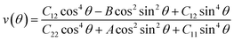
The Young's modulus Y(θ) and Poisson's ratio v(θ) of the Si4HX monolayers can be expressed as:52| | 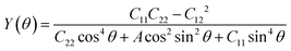 | (1) |
| |  | (2) |
where θ is the angle of the arbitrary direction with respect to the x-axis, A = (C11C22 − C122)/C66 − 2C12, and B = C11 + C22 − (C11C22 − C122)/C66. The elastic constants Ckl of the Si4HX monolayers can be found in Table 1. The Si4HX monolayers exhibit symmetry of the C3v space group, and crystals with this space group satisfy the following relationships: C11 = C22 and C66 = (C11 − C12)/2. Consequently, the Young's modulus and Poisson's ratio of these crystals can be simplified as:| | 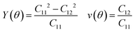 | (3) |
The concentric circles in polar coordinates shown in Fig. 3 indicate that the Si4HX monolayers exhibit isotropic Young's modulus and Poisson's ratio, which can be attributed to their isotropic lattice constants (a = b) of the Si4HX monolayers (which can be seen in Table 1). The Young's modulus of the Si4HBrFS (110.11 N m−1) is three times smaller than that of graphene (330 N m−1),53 indicating that these Si4HX monolayers exhibit flexible characteristics and have potential applications in flexible electronic devices. Soft 2D piezoelectric materials can more readily alter the intensity of their built-in electric fields under stress regulation, thereby more efficiently utilizing the enhanced built-in electric field to suppress the recombination of photogenerated carriers while accelerating carrier migration. This is precisely the advantage of piezoelectric-photocatalysts. Furthermore, as shown in Table 1, all Si4HX monolayers satisfy the Born–Huang criteria:54C11C12 − C122 > 0 and C66 > 0, demonstrating their mechanical stability.
 |
| | Fig. 3 (a) Young's modulus and (b) Poisson's ratio of the Si4HX monolayers, respectively. | |
3.3. Electronic properties
As depicted in Fig. 4, the energy band structures of the Si4HX monolayers indicate that they are indirect semiconductors, with the conduction band minimum (CBM) and valence band maximum (VBM) located at the high-symmetry points M and G, respectively. As shown in Fig. 1(a) and (b), in Si4HXFS, the distance between the upper two atomic layers and the lower two atomic layers decreases compared to that in Si4HXIS, leading to a change in the electron distribution between the initial and final states of the Si4HX monolayers (see Fig. S1 in the SI). The spatial distribution of the yellow electron accumulation region and the blue electron depletion region in Fig. S1 shows a significant difference between the two configurations. Moreover, the electronic band structures and PDOS, shown in Fig. 4, indicate that the interlayer distance variation simultaneously regulates the band alignment and orbital hybridization of the electronic states, comprehensively reflecting the synergistic regulation effect of the interlayer distance on electron transfer, accumulation, and electronic structure. Combining with Table 1, it is evident that the polarization intensity along the in-plane direction in the final state of the Si4HX monolayers is enhanced compared to that in the initial state. Consequently, the bandgaps of the Si4HX monolayers in the final state are reduced compared to those in the initial state. We also calculated the quasiparticle band edge positions and bandgaps using the G0W0 method, as shown in Table S2 of the SI. The G0W0 approach consistently yields larger bandgaps than both PBE and HSE06 methods across all materials, reflecting stronger quasiparticle energy corrections. This systematic broadening is crucial for the accurate assessment of light absorption capabilities. The VBM/CBM positions derived from HSE06 and G0W0 methods exhibit relatively consistent alignment trends across different materials. This validates the reliability of HSE06 for qualitative trend analysis while underscoring the role of G0W0 in the accurate determination of band edge positions when evaluating photocatalytic potential. The core of photocatalytic reactions lies in the generation of electron–hole pairs by semiconductor materials after absorbing photons, which drives redox reactions. The bandgap of the material directly determines its light absorption range and carrier separation efficiency. According to eqn (S1) and (S2) in the SI, as the bandgap decreases, the AM1.5 solar flux at the photon energy ℏω increases, leading to a higher solar-to-hydrogen (STH) conversion efficiency (the theoretical knowledge for calculating light absorption efficiency, carrier utilization efficiency, STH efficiency (ηSTH), and modified STH efficiency (ηcSTH)12 is provided in the SI). As shown in Table 2, the ηSTH of the Si4HClIS reaches as high as 29.46%, and the vacuum level-corrected STH efficiency (ηcSTH) also attains 26.53%. The ηSTH of the Si4HClFS further increases to an impressive 36.44%, with ηcSTH reaching 31.81%. These values far exceed those of most other 2D materials listed in Table S5 of the SI, highlighting the excellent photocatalytic water-splitting performance of the Si4HX monolayers.
 |
| | Fig. 4 The electronic band structures and projected density of states (PDOS) of (a) Si4HFIS, (b) Si4HFFS, (c) Si4HClIS, (d) Si4HClFS, (e) Si4HBrIS, and (f) Si4HBrFS monolayers calculated using the HSE06 functional. The Fermi level is set to zero. | |
Table 2 Carrier mobilities μx/y (cm2 V−1 s−1) along the x- and y-directions, light absorption efficiencies ηabs (%), carrier utilization efficiencies ηcu (%), solar-to-hydrogen (STH) efficiencies ηSTH (%), and modified ηcSTH (%) at pH = 0 for Si4HX monolayers
| Monolayer |
Carrier type |
μ
x
|
μ
y
|
η
abs
|
η
cu
|
η
STH
|
η
c
STH
|
| Si4HFIS |
Light hole |
2.07 × 10³ |
0.97 × 10³ |
61.14 |
48.83 |
29.86 |
24.68 |
| Heavy hole |
0.13 × 10³ |
37.51 |
| Electron |
2.00 × 10³ |
0.24 × 10³ |
|
|
| Si4HFFS |
Light hole |
4.17 × 10³ |
2.93 × 10³ |
70.48 |
52.22 |
36.81 |
28.86 |
| Heavy hole |
0.36 × 10³ |
0.18 × 10³ |
| Electron |
2.45 × 10³ |
0.37 × 10³ |
|
|
| Si4HClIS |
Light hole |
1.41 × 10³ |
0.80 × 10³ |
60.57 |
48.64 |
29.46 |
26.53 |
| Heavy hole |
77.55 |
21.88 |
| Electron |
0.50 × 10³ |
0.15 × 10³ |
|
|
| Si4HClFS |
Light hole |
1.69 × 10³ |
1.06 × 10³ |
70.48 |
51.70 |
36.44 |
31.81 |
| Heavy hole |
0.14 × 10³ |
58.90 |
| Electron |
1.63 × 10³ |
0.65 × 10³ |
|
|
| Si4HBrIS |
Light hole |
0.86 × 10³ |
0.77 × 10³ |
63.44 |
37.57 |
23.83 |
21.88 |
| Heavy hole |
42.04 |
19.03 |
| Electron |
1.34 × 10³ |
0.22 × 10³ |
|
|
| Si4HBrFS |
Light hole |
1.39 × 10³ |
1.38 × 10³ |
73.15 |
33.92 |
24.81 |
22.23 |
| Heavy hole |
93.72 |
51.10 |
| Electron |
1.72 × 10³ |
0.27 × 10³ |
3.4. Built-in field
The atomic layer sliding in the Si4HX monolayers does not alter the distribution of internal atoms along the out-of-plane direction. Therefore, the built-in electric field strengths along the out-of-plane direction (calculated through  50 and as shown in Table 1) and the out-of-plane piezoelectric stress coefficients e31 (see Table S5 in the SI) of the Si4HX monolayers are not affected by the transitions between their initial and final states. The built-in electric field can drive the migration of carriers along the out-of-plane direction within the 2D Janus material, prevent the recombination of photogenerated carriers, and enable them to migrate more rapidly to the material surface for participating in photocatalytic reactions, thereby demonstrating its advantages as a photocatalyst. Out-of-plane piezoelectricity is an effective means of regulating the built-in electric field strength of 2D materials through stress/strain. Therefore, we focus here on the out-of-plane piezoelectric coefficients of the Si4HX monolayers (the relevant theoretical knowledge is provided in the SI). As shown in Fig. 5(a), Si4HFIS exhibits the largest built-in electric field strength (3.23 × 10⁹ V m−1) and e31 value among the Si4HXIS monolayers, resulting in the strongest driving force for carrier migration along the out-of-plane direction and the highest efficiency in regulating the built-in electric field strength by stress. Compared to other 2D materials listed in Table S5 of the SI, the out-of-plane piezoelectric coefficients e31 of the Si4HX monolayers are relatively large, indicating their excellent out-of-plane piezoelectricity. The strength of the out-of-plane piezoelectricity in the Si4HXIS depends on the magnitude of the out-of-plane Born effective charges (BECs) Z33* of the internal Si4 and X atoms (as shown in Fig. 5(c), the Z33* values of other atoms are nearly identical). Furthermore, the Bader charge values of the Si4 and X atoms in the Si4HXIS, as shown in Fig. 5(d), reflect the amount of charge transfer between them, explaining the variation in their Z33* values.
 |
| | Fig. 5 (a) Ionic-contribute, electronic-contribute, and total out-of-plane piezoelectric stress coefficients e31 in Si4HX monolayers. (b) Out-of-plane piezoelectric strain coefficients d31 of Si4HX. (c) Z33* BECs and (d) Bader charges of each atom in the Si4HXIS monolayers, respectively. | |
3.5. Carrier mobility
We employed the Berry phase method to calculate the polarization intensity components along the x- and y-directions of the orthorhombic supercell (as depicted by the yellow dashed boxes in Fig. 1(a) and (b)) of the Si4HX monolayers. During the transition of the Si4HX monolayers from their initial to final states, the displacement directions of Si4 and X atoms are along the in-plane direction, leading to a flip and enhancement of the internal in-plane polarization. The theoretical approach for calculating carrier mobility using deformation potential theory can be found in the SI. Herein, we calculated the carrier transport properties of the Si4HX monolayers also using their orthorhombic supercells, aligning the x- and y-transport directions with the high-symmetry paths in the Brillouin zone and facilitating the application of uniaxial strain along these axes. As shown in Fig. 6, the G → X and G → Y paths in Si4HX monolayers correspond to the x- and y-directions, respectively. For effective mass calculations, the primitive cell's energy band structure serves as the standard. In the Si4HX, the CBM of their unit cells is non-degenerate, while the VBM exhibits two-fold degeneracy. In this case, differences in effective mass and carrier mobility between light and heavy holes have to be considered.
 |
| | Fig. 6 (a) The high-symmetry paths within the Brillouin zone of the orthorhombic supercell of the Si4HX monolayers. The electronic band structures of the orthorhombic supercell of (b)–(g) Si4HX monolayers at the PBE level. The band edge positions (VBM and CBM) are expressed as green and blue dots, respectively. | |
The presence of light holes plays a crucial role in enhancing the carrier mobility of these 2D materials. As shown in Table 2 and Table S3 in the SI, the carrier mobilities of the Si4HX monolayers along the x-direction are significantly higher than that along the y-direction, exhibiting anisotropy. Furthermore, the carrier mobilities of the Si4HXFS are generally higher than that of the corresponding Si4HXIS, owing to the reduced carrier effective mass |mx/y| in the final state compared to the initial state. The structural transformation of the Si4HX monolayers from their initial to final states enhances the in-plane polarization intensity (particularly along the x-direction), better driving the carriers and thereby increasing their mobilities. High carrier mobility along the in-plane direction reduces photogenerated charge recombination, improves charge separation efficiency, and consequently enhances the photocatalytic performance of the Si4HX monolayers. This structural advantage enables efficient lateral redistribution of carriers, which balances surface concentration gradients and minimizes localized electron–hole recombination, further optimizing catalytic activity.
3.6. Optical and photocatalytic properties
The band edge positions (VBM and CBM) of the Si4HX monolayers are shifted relative to the vacuum energy level. As shown in Fig. 7(a)–(f) and Table S4 in the SI, at pH = 0, the vacuum energy level-corrected VBM and CBM (denoted as EvacVBM and EvacCBM, respectively) of the Si4HX monolayers are both lower than the OER potential (−5.67 eV) and higher than the HER potential (−4.44 eV). This indicates that the Si4HX monolayers possess the capability for overall photocatalytic water splitting at pH = 0. Additionally, according to the Nernst equation (EOER/HER = −5.67/−4.44 eV + 0.059 eV × pH),55 as illustrated in Fig. 7(g), the overall photocatalytic water splitting capability of the Si4HX monolayers spans from pH 0 to 14, qualifying them as wide-pH-range photocatalysts. For photocatalysts, the ability to absorb sunlight is crucial. To account for the excitonic effects within the 2D materials, we employed the G0W0 + Bethe–Salpeter equation (BSE) method to calculate the optical absorption coefficients of the Si4HX monolayers. As depicted in Fig. 7(h), the peak optical absorption coefficients of Si4HXFS in the ultraviolet range are enhanced compared to those of Si4HXIS. This is because the final state obtained through atomic layer sliding narrows the bandgap, allowing more low-energy photons to excite electron transitions and thereby enhancing ultraviolet light absorption efficiency. Notably, the Si4HClIS exhibits an optical absorption coefficient as high as 17.28% in the visible light range, significantly outperforming graphene (2.30%), MoS2 (14.87%), WS2 (9.79%), MoSe2 (4.62%), and WSe2 (10.05%) monolayers.56,57 It is evident that the Si4HX monolayers possess excellent light absorption capabilities. Particularly, the final state structures after transformation, as shown in Table 2, demonstrate a marked improvement in light absorption efficiency at pH = 0 compared to their initial states, thereby enhancing their solar energy utilization efficiency (a comparison of the light absorption efficiencies of Si4HX monolayers with other 2D materials is provided in Table S5 of the SI).
 |
| | Fig. 7 (a)–(f) Electrostatic potentials along the z-direction for Si4HX monolayers calculated using the HSE06 functional. Evac1/2 denotes the vacuum energy levels at the upper/lower surfaces of the structures. ΔΦ represents the electrostatic potential difference between the upper and lower surfaces of the structure. The orange dashed lines indicate the oxidation and reduction potentials of water at pH = 0. The black arrows indicate the direction of the built-in electric field within the structures. The blue and green boxes represent the positions of the CBM and VBM, respectively, after vacuum energy level correction. (g) Positions of the vacuum energy level-corrected band edges of Si4HX monolayers relative to the redox potentials of water at different pH values. The blue and green hemispheres represent the vacuum energy level-corrected band edge positions of the structure. (h) In-plane optical absorption coefficients of Si4HX monolayers calculated using the GW + BSE method. | |
Based on our discussion, Janus Si4HX monolayers exhibit suitable band gaps and favorable band alignments, along with high carrier mobilities and strong optical absorption abilities, meeting the criteria for photocatalytic water splitting. Moreover, the electronegativity of the X layer exceeds that of the H layer in Si4HX monolayers. Consequently, the built intrinsic field is oriented from the H layer toward the X layer (from the top pointing to the bottom). Therefore, the HER occurs in the electron rich H layer, and the OER occurs in the hole-rich X layer. It is widely recognized that the built intrinsic field of ΔΦ alters the overpotential limits of Ue and Uh, as calculated by Ue = (ECBM − EH+/H2)/e and Uh = (EO2/H2O − EVBM)/e, thereby enhancing the driving forces to facilitate the HER and OER. These results indicate that photogenerated carriers in monolayers can promote redox reactions and contribute to the reduction of energy loss. As the initial and vital step, the adsorption of the water molecule on the Si4HX monolayers is discussed by examining the adsorption energy. Two possible adsorption sites are proposed for screening the most stable adsorption configuration. In Fig. 8(a), all adsorption energies in two cases are negative, which are provided in Table S4 of the SI, and the adsorption energies on the top side are higher than those on the bottom side. This indicates that water molecules are more inclined to adsorb at the bottom site. The proposed photocatalytic pathways of two half-reactions and the corresponding adsorbed intermediates of H*, OH*, O*, and OOH* are displayed in Fig. 8(b). The Gibbs free energy change of the HER and OER is calculated to further evaluate the photocatalytic activity of the Si4HX monolayers (see the SI for computational details).
 |
| | Fig. 8 (a) Adsorption energies of water molecules on Si4HX monolayers at different sites. (b) The water splitting (HER and OER) processes for Janus Si4HX. The free energy diagram of the HER under (c) dark (U = 0) and (d) light (U = Ue) conditions for Si4HX. (e)–(j) The free energy of the OER for Si4HX. | |
Fig. 8(c) and (d) present the Gibbs free energy diagrams for the two steps of the HER under dark and light conditions. The H* intermediate state is the rate-determining step. Si4HX monolayers need to overcome an energy barrier of 0.95–1.11 eV under the dark, but under the voltage effect provided by photogenerated electrons, ΔG decreases to negative values (except for the Si4HBrFS monolayer), which means that the HER can proceed spontaneously under light. For the OER, Fig. 8(e)–(j) present the free energy evolution from * to OH*, O*, OOH*, and then to O2. Taking Si4HFIS as an example, the energy barrier can be effectively reduced under Uh = 1.77 V, and other Si4HX monolayers also show similar trends under different potentials.
4. Conclusions
In summary, we have designed a series of Janus silicon-based diamane Si4HX structures that exhibit dynamic, thermodynamic, and mechanical stability. By leveraging the concept of atomic layer sliding, we transformed the Si4HX monolayers from their initial states to final states, resulting in enhanced physical properties that characterize their photocatalytic performance. The reduction in the bandgap of the final state compared to the initial state not only improves solar-to-hydrogen efficiency but also enables more low-energy photons to excite electron transitions, thereby enhancing ultraviolet light absorption. Simultaneously, the enhanced in-plane ferroelectric polarization in the final state further drives carrier separation, increasing carrier mobility. The synergistic effects of these improvements collectively enhance the photocatalytic performance of the Si4HX monolayers. Finally, the strong internal built-in electric fields within the Si4HX monolayers, combined with their excellent out-of-plane piezoelectric properties, provide a greater driving force for carriers under stress/strain conditions. This facilitates rapid migration of carriers to the material surface, where they participate in photocatalytic reactions and suppress recombination. These features highlight the advantages of the Si4HX monolayers as 2D piezoelectric photocatalysts.
Conflicts of interest
The authors have no conflicts to disclose.
Data availability
The authors confirm that the data supporting the findings of this study are available within the article or its supplementary information (SI). Supplementary information is available. See DOI: 10.1039/d5cp04059k.
Acknowledgements
This work was supported by the Natural Science Foundation of China (Grant No. 11974139 and 11574116).
References
- P. Zhou, I. A. Navid, Y. Ma, Y. Xiao, P. Wang, Z. Ye, B. Zhou, K. Sun and Z. Mi, Nature, 2023, 613, 66–70 CrossRef CAS PubMed.
- Y. Gao, Q. Zhang, W. Hu and J. Yang, ACS Nano, 2024, 18, 19381–19390 CrossRef CAS PubMed.
- W. Zhu, X. Qiu, V. Iancu, X.-Q. Chen, H. Pan, W. Wang, N. M. Dimitrijevic, T. Rajh, H. M. Meyer, M. P. Paranthaman, G. M. Stocks, H. H. Weitering, B. Gu, G. Eres and Z. Zhang, Phys. Rev. Lett., 2009, 103, 226401 CrossRef.
- D. H. Ozbey, M. E. Kilic and E. Durgun, Phys. Rev. Appl., 2022, 17, 034043 CrossRef CAS.
- V. Chakrapani, J. C. Angus, A. B. Anderson, S. D. Wolter, B. R. Stoner and G. U. Sumanasekera, Science, 2007, 318, 1424–1430 CrossRef CAS PubMed.
- C.-F. Fu, Q. Luo, X. Li and J. Yang, J. Mater. Chem. A, 2016, 4, 18892–18898 RSC.
- Y. Cai, G. Zhang and Y.-W. Zhang, J. Am. Chem. Soc., 2014, 136, 6269–6275 CrossRef CAS PubMed.
- C.-J. Tong, L. Li, L.-M. Liu and O. V. Prezhdo, J. Am. Chem. Soc., 2020, 142, 3060–3068 CrossRef CAS PubMed.
- C. R. Cox, J. Z. Lee, D. G. Nocera and T. Buonassisi, Proc. Natl. Acad. Sci. U. S. A., 2014, 111, 14057–14061 CrossRef CAS.
- X. Ma, X. Wu, H. Wang and Y. Wang, J. Mater. Chem. A, 2018, 6, 2295–2301 RSC.
- X. Li, Z. Li and J. Yang, Phys. Rev. Lett., 2014, 112, 018301 CrossRef PubMed.
- C.-F. Fu, J. Sun, Q. Luo, X. Li, W. Hu and J. Yang, Nano Lett., 2018, 18, 6312–6317 CrossRef CAS PubMed.
- K. Chang, J. Liu, H. Lin, N. Wang, K. Zhao, A. Zhang, F. Jin, Y. Zhong, X. Hu, W. Duan, Q. Zhang, L. Fu, Q.-K. Xue, X. Chen and S.-H. Ji, Science, 2016, 353, 274–278 CrossRef CAS PubMed.
- F. Liu, L. You, K. L. Seyler, X. Li, P. Yu, J. Lin, X. Wang, J. Zhou, H. Wang, H. He, S. T. Pantelides, W. Zhou, P. Sharma, X. Xu, P. M. Ajayan, J. Wang and Z. Liu, Nat. Commun., 2016, 7, 12357 CrossRef CAS.
- Q. Wang, T. Hisatomi, Q. Jia, H. Tokudome, M. Zhong, C. Wang, Z. Pan, T. Takata, M. Nakabayashi, N. Shibata, Y. Li, I. D. Sharp, A. Kudo, T. Yamada and K. Domen, Nat. Mater., 2016, 15, 611–615 CrossRef CAS.
- J. Liu, Y. Liu, N. Liu, Y. Han, X. Zhang, H. Huang, Y. Lifshitz, S.-T. Lee, J. Zhong and Z. Kang, Science, 2015, 347, 970–974 CrossRef CAS PubMed.
- L. Ju, J. Shang, X. Tang and L. Kou, J. Am. Chem. Soc., 2020, 142, 1492–1500 CrossRef CAS.
- Y.-X. Du, Y. Mu, W.-M. Liu, X. Jia, J.-H. Lin and T. Zhang, Appl. Surf. Sci., 2025, 702, 163289 CrossRef CAS.
- X. Shang, H.-N. Zhang, S.-T. Liu, D.-S. Tang, Q.-W. He, J.-H. Wang, D.-Y. Zhu, F.-C. Liu and X.-C. Wang, Appl. Phys. Lett., 2024, 124, 172901 CrossRef CAS.
- X. Shang, D.-S. Tang, Q.-W. He, H.-N. Zhang, F.-C. Liu and X.-C. Wang, Appl. Phys. Lett., 2023, 123, 192901 CrossRef CAS.
- W. Liu, L. Zhang, X. Liu, X. Liu, X. Yang, S. Miao, W. Wang, A. Wang and T. Zhang, J. Am. Chem. Soc., 2017, 139, 10790–10798 CrossRef CAS.
- B. Anasori, M. R. Lukatskaya and Y. Gogotsi, Nat. Rev. Mater., 2017, 2, 16098 CrossRef CAS.
- P. V. Bakharev, M. Huang, M. Saxena, S. W. Lee, S. H. Joo, S. O. Park, J. Dong, D. C. Camacho-Mojica, S. Jin, Y. Kwon, M. Biswal, F. Ding, S. K. Kwak, Z. Lee and R. S. Ruoff, Nat. Nanotechnol., 2020, 15, 59–66 CrossRef CAS.
- G. Kresse and J. Furthmüller, Phys. Rev. B: Condens. Matter Mater. Phys., 1996, 54, 11169–11186 CrossRef CAS PubMed.
- G. Kresse and J. Furthmüller, Comput. Mater. Sci., 1996, 6, 15–50 CrossRef CAS.
- P. E. Blöchl, Phys. Rev. B: Condens. Matter Mater. Phys., 1994, 50, 17953–17979 CrossRef PubMed.
- J. P. Perdew, K. Burke and M. Ernzerhof, Phys. Rev. Lett., 1996, 77, 3865–3868 CrossRef CAS PubMed.
- S. Grimme, J. Antony, S. Ehrlich and H. Krieg, J. Chem. Phys., 2010, 132, 154104 CrossRef PubMed.
- D. R. Hamann, Phys. Rev. B: Condens. Matter Mater. Phys., 2013, 88, 085117 CrossRef.
- A. Baroni, F. Pacaud, M. Salanne, M. Micoulaut, J.-M. Delaye, A. Zeidler, P. S. Salmon and G. Ferlat, J. Chem. Phys., 2019, 151, 224508 CrossRef PubMed.
- G. Henkelman, B. P. Uberuaga and H. Jónsson, J. Chem. Phys., 2000, 113, 9901–9904 CrossRef CAS.
- D. Alfè, Comput. Phys. Commun., 2009, 180, 2622–2633 CrossRef.
- M. Yagmurcukardes and F. M. Peeters, Phys. Rev. B, 2020, 101, 155205 CrossRef CAS.
- F. Eriksson, E. Fransson and P. Erhart, Adv. Theory Simul., 2019, 2, 045415 Search PubMed.
- T. A. Manz, RSC Adv., 2017, 7, 45552–45581 RSC.
- J. Bardeen and W. Shockley, Phys. Rev., 1950, 80, 72–80 CrossRef CAS.
- J. Harl and G. Kresse, Phys. Rev. B: Condens. Matter Mater. Phys., 2008, 77, 045136 CrossRef.
- J. Klimeš, M. Kaltak and G. Kresse, Phys. Rev. B: Condens. Matter Mater. Phys., 2014, 90, 075125 CrossRef.
- C. Xia, W. Xiong, J. Du, T. Wang, Y. Peng and J. Li, Phys. Rev.
B, 2018, 98, 165424 CrossRef CAS.
- L. Ju, M. Bie, X. Tang, J. Shang and L. Kou, ACS Appl. Mater. Interfaces, 2020, 12, 29335–29343 CAS.
- P. Jamdagni, A. Kumar, S. Srivastava, R. Pandey and K. Tankeshwar, Phys. Chem. Chem. Phys., 2022, 24, 22289–22297 RSC.
- P. Wang, Y. X. Zong, H. Liu, H. Y. Wen, H. B. Wu and J. B. Xia, J. Mater. Chem. C, 2021, 9, 4989–4999 RSC.
- X. Z. Tan, Q. Chen, Y. C. Liang, Z. A. Tian, T. H. Gao and Q. Xie, Int. J. Hydrogen Energy, 2024, 51, 222–230 CrossRef CAS.
- Y. X. Du, Y. Mu, W. M. Liu, X. Jia, J. H. Lin and T. Zhang, Appl. Surf. Sci., 2025, 702, 124857 CrossRef.
- L. Pan, Y. L. Wan, Z. Q. Wang, H. Y. Geng and X. R. Chen, J. Appl. Phys., 2023, 134, 085105 CrossRef CAS.
- Y. R. Ying, Z. Z. Lin and H. T. Huang, ACS Energy Lett., 2023, 8, 1416–1423 CrossRef CAS.
- L. Ju, J. Shang, X. Tang and L. Z. Kou, J. Am. Chem. Soc., 2020, 142, 1492–1500 CrossRef CAS PubMed.
- L. Liu, T. Li, X. Gong, H. Wen, L. Zhou, M. Feng, H. Zhang, N. Zou, S. Wu, Y. Li, S. Zhu, F. Zhuo, X. Zou, Z. Hu, Z. Ding, S. Fang, W. Xu, X. Hou, K. Zhang, G. Long, L. Tang, Y. Jiang, Z. Yu, L. Ma, J. Wang and X. Wang, Nat. Mater., 2025, 24, 1195–1202 CrossRef CAS PubMed.
- J. Liu, J. Zhao, T. Li, D. Ji, L. Dai, L. Li, Z. Wei, J. Li, Q. Wang, H. Yu, L. Zhou, Y. Chen, F. Wu, M. Zhu, H. Sun, Y. Li, S. Zhang, J. Tian, X. Zhang, N. Lu, X. Bai, Z. Cao, S. Lin, S. Wang, D. Shi, N. Li, L. Du, W. Yang, L. Xian and G. Zhang, Nat. Electron., 2025, 390, 837 Search PubMed.
- Y.-Q. Li, D.-S. Tang, Q.-W. He, X. Shang and X.-C. Wang, Appl. Phys. Lett., 2023, 122, 193023 Search PubMed.
- M. Yagmurcukardes and F. M. Peeters, Phys. Rev. B, 2020, 101, 155205 CrossRef CAS.
- M. Yagmurcukardes, C. Sevik and F. M. Peeters, Phys. Rev. B, 2019, 100, 045415 CrossRef CAS.
- M. Yagmurcukardes, R. T. Senger, F. M. Peeters and H. Sahin, Phys. Rev. B, 2016, 94, 245407 CrossRef.
- J. Wang, S. Yip, S. R. Phillpot and D. Wolf, Phys. Rev. Lett., 1993, 71, 4182–4185 CrossRef CAS PubMed.
- L. Pan, T. Zhang, C. E. Hu, X. R. Chen and H. Y. Geng, J. Mater. Chem. A, 2022, 10, 22676–22685 RSC.
- K. R. Paton and J. N. Coleman, Carbon, 2016, 107, 733–738 CrossRef CAS.
- R. R. Nair, P. Blake, A. N. Grigorenko, K. S. Novoselov, T. J. Booth, T. Stauber, N. M. R. Peres and A. K. Geim, Science, 2008, 320, 1308 CrossRef CAS PubMed.
Footnote |
| † These authors contributed equally to this work. |
|
| This journal is © the Owner Societies 2026 |
Click here to see how this site uses Cookies. View our privacy policy here. 
 a,
Chu-Chu
Liu†
a,
Pan
Ma
a,
Xiao
Shang
a,
Hai-Bin
Du
b,
Xian-Yu
Hu
c,
Lu-Chao
Du
*a and
Fu-Chun
Liu
*a
a,
Chu-Chu
Liu†
a,
Pan
Ma
a,
Xiao
Shang
a,
Hai-Bin
Du
b,
Xian-Yu
Hu
c,
Lu-Chao
Du
*a and
Fu-Chun
Liu
*a


 50 and as shown in Table 1) and the out-of-plane piezoelectric stress coefficients e31 (see Table S5 in the SI) of the Si4HX monolayers are not affected by the transitions between their initial and final states. The built-in electric field can drive the migration of carriers along the out-of-plane direction within the 2D Janus material, prevent the recombination of photogenerated carriers, and enable them to migrate more rapidly to the material surface for participating in photocatalytic reactions, thereby demonstrating its advantages as a photocatalyst. Out-of-plane piezoelectricity is an effective means of regulating the built-in electric field strength of 2D materials through stress/strain. Therefore, we focus here on the out-of-plane piezoelectric coefficients of the Si4HX monolayers (the relevant theoretical knowledge is provided in the SI). As shown in Fig. 5(a), Si4HFIS exhibits the largest built-in electric field strength (3.23 × 10⁹ V m−1) and e31 value among the Si4HXIS monolayers, resulting in the strongest driving force for carrier migration along the out-of-plane direction and the highest efficiency in regulating the built-in electric field strength by stress. Compared to other 2D materials listed in Table S5 of the SI, the out-of-plane piezoelectric coefficients e31 of the Si4HX monolayers are relatively large, indicating their excellent out-of-plane piezoelectricity. The strength of the out-of-plane piezoelectricity in the Si4HXIS depends on the magnitude of the out-of-plane Born effective charges (BECs) Z33* of the internal Si4 and X atoms (as shown in Fig. 5(c), the Z33* values of other atoms are nearly identical). Furthermore, the Bader charge values of the Si4 and X atoms in the Si4HXIS, as shown in Fig. 5(d), reflect the amount of charge transfer between them, explaining the variation in their Z33* values.


