
 Open Access Article
 This Open Access Article is licensed under a Creative Commons Attribution-Non Commercial 3.0 Unported Licence
Atomic layer deposition of metal halide perovskites: chemistry, growth mechanisms, and emerging prospects
Joshua Sraku Adu
ab,
George Kwesi Asare
ab and
Helen Hejin Park
 *abc
*abc
aAdvanced Materials Division, Korea Research Institute of Chemical Technology (KRICT), Daejeon 34114, Republic of Korea
bDepartment of Advanced Materials and Chemical Engineering, University of Science and Technology (UST), Daejeon 34113, Republic of Korea
cDepartment of Chemical and Biological Engineering, Hanbat National University, Daejeon 34158, Republic of Korea. E-mail: hhpark@hanbat.ac.kr
First published on 12th March 2026
Abstract
Atomic layer deposition (ALD) offers exceptional control over film thickness, composition, and interface quality, making it an attractive approach for constructing metal-halide perovskite absorber layers. While ALD is now well established for transport layers and interfacial passivation, its direct use in synthesizing perovskite precursor layers such as lead iodide (PbI2) remains comparatively early-stage. This short review examines recent developments in ALD halide perovskite growth, post-deposition conversion strategies, and the emerging prospects of fully vapor-phase perovskite growth. We discuss limitations in precursor design, iodination chemistry, temperature compatibility, and device integration while identifying short-term opportunities where ALD uniquely enables advances in perovskite photovoltaics, displays, and transistors. Finally, we offer a forward-looking assessment of the breakthroughs required for ALD to evolve from a niche method into a scalable deposition pathway for commercialization.
 Joshua Sraku Adu | Joshua Sraku Adu is a PhD candidate in the Department of Advanced Materials and Chemical Engineering at the KRICT School, University of Science and Technology (UST), Daejeon, Republic of Korea. He joined the perovskite research team at the Korea Research Institute of Chemical Technology (KRICT) in 2022 under the supervision of Dr Helen Hejin Park and has recently become part of the organic photodetector research group at the same institute. Joshua received his BSc degree in Materials Engineering from Kwame Nkrumah University of Science and Technology (KNUST), Ghana, in 2020. Following his undergraduate studies, he served as a teaching and research assistant in the Department of Materials Engineering at KNUST during the academic year 2020–2021. His current research focuses on the application of atomic layer deposition (ALD) techniques to enhance the stability and performance of perovskite solar cells. In addition, he investigates strategies to improve the stability and responsivity of perovskite-based photodetectors. |
 George Kwesi Asare | George Kwesi Asare is a PhD candidate in the Department of Advanced Materials and Chemical Engineering at the University of Science and Technology (UST) and a student researcher in the Advanced Materials Division at the Korea Research Institute of Chemical Technology (KRICT) in Daejeon, Korea. He was previously under the supervision of Dr Helen Hejin Park. He received his BSc in Materials Engineering from Kwame Nkrumah University of Science and Technology (KNUST), Ghana, in 2021. His past research focused on atomic layer deposition techniques for highly efficient and stable space compatible perovskite solar cells. He is currently focused on device structures, performance metrics, and improving the stability and sensitivity of perovskite photodetectors. |
 Helen Hejin Park | Helen Hejin Park is an Assistant Professor at Hanbat National University in the Department of Chemical and Biological Engineering in Daejeon, Korea. She was previously a Principal Research Scientist and Senior Researcher in the Advanced Materials Division at the Korea Research Institute of Chemical Technology (KRICT) and an Associate Professor at the University of Science and Technology (UST). Dr Park received her BS in Chemical Engineering from the University of Rochester in 2008 and her PhD in Applied Physics from Harvard University in 2015. She was a postdoctoral researcher at the U.S. Naval Research Laboratory from 2015 to 2017. She joined KRICT in 2017, UST, in 2022, and Hanbat in 2026. Dr Park's past research experience includes the development of Earth-abundant and non-toxic thin-film solar cells and transition metal oxides for switching applications. Her current research area includes atomic layer deposition techniques for highly stable perovskite solar cells and space applications. She has been cited over 3200 times. |
1. Introduction: ALD as an emerging platform for vapor-phase perovskite growth
Atomic layer deposition has undergone a notable transition in its perceived role within the perovskite photovoltaics community, progressing from its familiar position as a precision tool for depositing transport layers and surface passivation films to an increasingly credible strategy for constructing entire metal-halide perovskite absorbers via vapor-phase routes. This transition has been enabled by the unique capabilities of ALD's self-limiting surface chemistry, sub-nanometer thickness control, perfect conformality over textured or porous surfaces, and the capacity to integrate with low-temperature processing windows.1–10 These characteristics align closely with the stringent structural and electronic requirements of perovskite absorber layers, where film continuity, nucleation control, and defect suppression directly influence carrier mobility, trap density, and eventual device operation. As the performance, scale, and reliability demands of perovskite photovoltaics continue to increase, the need for deterministic, repeatable, and highly uniform vapor-phase methods has become more compelling. Although solution processing and thermal co-evaporation remain the dominant methods for producing perovskite films, the rapid emergence of ALD PbI2, lead bromide (PbBr2), and mixed-halide processes reflects an accelerating interest in reshaping the perovskite fabrication landscape by incorporating the atomic-level precision characteristic of microelectronics manufacturing.11–16Early engagement of ALD with perovskite technology was centered on transport layers, where ALD titanium dioxide (TiO2), tin dioxide (SnO2), and aluminum oxide (Al2O3) layers have demonstrated exceptional reproducibility, interfacial quality, and improved device stability under moisture, oxygen, thermal, and ultraviolet (UV) stress.17–21 These films brought unprecedented control to the electron-transport layers of early perovskite devices, clarifying the role of surface energetics, interface dipoles, and dielectric passivation. The demonstrated stability enhancement from ALD Al2O3, particularly its ability to suppress mobile ion migration and passivate deep-level traps at the perovskite surface, helped catalyze the community's broader interest in ALD as more than a merely supporting technology.22–26 This momentum was soon extended to direct halide precursor deposition. Researchers reasoned that if ALD could deliver oxide films of extremely high quality and stability, and if lead halide layers could be grown with commensurate precision, it might be possible to construct extremely uniform inorganic frameworks that could later undergo gentle organic incorporation to form high-quality perovskite lattices. Such hybrid vapor-conversion strategies show the potential to solve long-standing problems of solution processing, including irregular nucleation, inhomogeneous drying, rapid crystallization that traps defects, and the inherent difficulty of coating rough or highly textured surfaces with perfect uniformity.27
2. Atomic-scale chemistry and process constraints governing ALD metal-halide growth
2.1. ALD halide growth pathways and framework
An important early demonstration of ALD-templated perovskite formation predates the first direct ALD PbI2 processes. In 2014–2015, Sargent and co-workers employed ALD-grown PbS as a conformal scaffold, subsequently converting it to PbI2 through I2 vapor exposure and finally to MAPbI3 via solution-phase MAI treatment. This multi-step approach highlighted one of ALD's most compelling advantages: the ability to create uniform, conformal inorganic templates that could later undergo controlled halide and organic conversion. Although the halide and perovskite formation steps were performed outside the ALD reactor, the study established the conceptual foundation for ALD-enabled perovskite templating and conformal absorber formation in complex geometries.28These developments are crystallized into two distinct conceptual frameworks for ALD-based perovskite fabrication. The first – hybrid ALD perovskite formation – has proven experimentally accessible and is now the dominant approach pursued across laboratories. In this route, an inorganic lead halide layer such as PbI2 is deposited using ALD and subsequently converted into a perovskite absorber by exposing it to organic iodides such as methylammonium iodide (MAI), formamidinium iodide (FAI), or inorganic cesium iodide (CsI), either through vapor-phase diffusion or thermal annealing under controlled partial pressures. The appeal of this method lies in its modularity: inorganic deposition and organic or inorganic conversion are chemically decoupled, providing unprecedented control over film thickness, coverage, and stoichiometry in the inorganic phase prior to conversion. The second framework envisions a fully direct ALD route in which lead, halide, and organic components are sequentially dosed and reacted within a single reactor to form the ABX3 perovskite structure in situ. Although conceptually elegant and aligned with classical ALD principles, this method remains unrealized due to the absence of volatile, self-limiting, and thermally compatible organic A-site precursors capable of participating in low-temperature ALD reactions without decomposition or desorption. The gulf between theoretical possibility and practical implementation remains wide, but it has motivated a surge of research into low-temperature halogenation chemistry, non-corrosive iodine sources, plasma-assisted conversion, and radically redesigned lead precursor families.
2.2. Lead precursor chemistry and surface reaction limitations
The chemical challenge of ALD halide perovskites begins with the lead precursors themselves, which sit at the core of any attempt to construct a reliable ALD route for PbI2 or related metal-halide perovskite frameworks. To date, the most widely investigated precursor families, β-diketonates and amidinates, have each revealed distinct benefits and intrinsic limitations that collectively illustrate the chemical fragility of low-temperature halogenation in the presence of bulky organic ligands.29 β-Diketonate complexes such as lead bis(2,2,6,6-tetramethyl-3,5-heptanedionate) (Pb(tmhd)2), lead bis(2,2-dimethyl-6,6,7,7,8,8-hexafluoro-3,5-octanedionate) (Pb(fod)2), and lead bis(hexafluoroacetylacetonate) (Pb(hfac)2) have gained early prominence due to their well-established vapor-phase delivery, moderate thermal stability, and predictable ligand-exchange behavior on hydroxylated or halogenated surfaces.30,31 These precursors were originally optimized for oxide ALD, where deposition temperatures between 180 and 300 °C allow the complete ligand removal and facilitate clean metal–oxygen bond formation. When translated to the perovskite-compatible regime (<120 °C), their reaction pathways shift considerably: ligand elimination becomes kinetically hindered, the equilibrium between surface-bound and gas-phase species becomes less favorable, and the resulting Pb–X (X = I, Br, Cl, S) framework forms with reduced ligand-exchange completeness.11 Several studies have confirmed that residual tmhd or fod fragments remain embedded within the forming PbI2 lattice under low-temperature cycling, leading to amorphous growth, suppressed crystallization, and reduced halide diffusivity. Because ALD relies on repeated cycles of chemisorption and ligand displacement, even a small fraction of unreacted β-diketonate groups can accumulate over tens or hundreds of cycles, ultimately influencing nucleation density, surface roughness, and conversion efficiency in downstream iodide-vapor processes.32,33Although amidinate ligands have become a cornerstone of precursor design for many ALD processes, particularly for metals such as titanium (Ti), zirconium (Zr), hafnium (Hf), and tin (Sn), their application to lead halide ALD remains largely prospective. Lead amidinate complexes such as lead bis(N,N′-diisopropylacetamidinate) (Pb(amd)2) or lead bis(isopropyl-amidinate) (Pb(iPr-amd)2) have been proposed as suitable candidates because, in principle, their strong bidentate N-chelation and relatively compact ligand geometry could provide improved volatility, higher thermal stability, and cleaner ligand-removal pathways compared to bulky β-diketonates. These attributes make amidinates attractive from a mechanistic standpoint: they can suppress β-hydride elimination, resist premature surface decomposition, and support uniform chemisorption at lower temperatures better than many established Pb precursors. However, no experimentally validated ALD cycles for PbI2 based on amidinate ligands have yet been reported, and their behavior under perovskite-compatible thermal budgets remains untested. This introduces an important caveat: even if amidinate complexes can, in theory, undergo complete ligand dissociation at temperatures of 130–150 °C, such conditions already exceed the stability limits of MA+ and FA+ cations and approach the decomposition threshold of iodide-rich intermediates. Thus, amidinate-based lead chemistry should presently be viewed as an attractive direction for future exploration rather than an established ALD route, with the perovskite temperature window imposing stringent constraints on any eventual implementation. The broader challenge remains the same, namely designing a Pb precursor that couples clean, self-limiting adsorption with efficient halogenation at ≤120 °C without compromising stoichiometry, film density, or crystallinity.
The drive toward low-temperature ALD strategies for halide perovskites extends beyond any single cation or halide system and reflects a broader need to reconcile precursor reactivity with the narrow thermal tolerance of hybrid and inorganic perovskites. Approaches explored thus far include Cs-based halide chemistry, radical-assisted iodination, modified lead precursor families such as amidinates, and spatial ALD variants designed to reduce residence times. Collectively, these strategies aim to decouple reaction completeness from substrate temperature, which remains the central bottleneck in vapor-phase perovskite synthesis. While still largely prospective in the context of PbI2 ALD, amidinate-based lead precursors represent a rational chemical direction. Their stronger chelation and reduced ligand mass relative to β-diketonates may lower the activation barrier for ligand removal under halide-rich conditions. Importantly, amidinates have demonstrated clean, self-limiting behavior in low-temperature ALD of other metal systems, suggesting that analogous Pb complexes could enable improved growth saturation below 120 °C. However, systematic thermogravimetric and in situ surface studies remain absent for Pb amidinate–iodine cycles. Future work must therefore establish volatility, decomposition pathways, and halogenation kinetics under perovskite-compatible conditions before these precursors can transition from conceptual promise to practical ALD routes.
Alkyl-lead precursors, including diethyl lead (Pb(C2H5)2) and dimethyl lead (Pb(CH3)2) analogues, are in principle attractive due to their inherent reactivity and theoretical ability to undergo direct Pb–I bond formation upon exposure to iodine donors. However, in practice, they do have severe drawbacks: thermal instability, pyrophoric behavior, a strong tendency to generate parasitic metallic lead or PbOx via reductive decomposition, and incompatibility with reactor materials under ALD cycling.34–36 Their decomposition can occur auto-catalytically, leading to uncontrolled nucleation, particle formation, and in extreme cases, corrosion or irreversible contamination of ALD reactor walls. Additionally, the surface chemistry of alkyl-lead species is notoriously difficult to control under the low-temperature, halide-rich environment required for perovskite precursor fabrication. As a result, the field has moved away from alkyl-lead reagents despite their nominal reactivity advantages.34,37
2.3. Iodine delivery, halogenation kinetics, and ligand-exchange barriers
The iodine precursor presents an equally complex challenge, one that extends far beyond simple precursor reactivity and into the fundamental surface kinetics that govern nucleation, ligand exchange, and complete halogen termination within the ALD cycle. Hydroiodic acid (HI), often considered the benchmark for iodine delivery in ALD PbI2 processes, remains appealing primarily because of its exceptionally strong reducing and halogenating capability. HI readily protonates and displaces organic ligands on adsorbed Pb(II) species, forming Pb–I bonds with high completeness even at low temperatures. In principle, this makes HI an ideal candidate for low-temperature ALD cycles where thermal budgets are constrained by the fragility of organic perovskite intermediates.38 However, the same chemical aggressiveness that makes HI effective also renders it extraordinarily corrosive, aggressively attacking stainless steel, aluminum, and many elastomeric components commonly used in ALD reactors.30,31 The constant risk of chamber etching, precursor-line degradation, and unwanted formation of iodine-rich residues on reactor walls severely complicates operational stability. Moreover, HI can participate in uncontrolled reactions with co-adsorbed species or reactive ligands, generating volatile byproducts that disrupt self-limiting growth.11,30,39 These practical and chemical hazards have significantly limited the adoption of HI-based ALD halogenation beyond tightly controlled laboratory-scale demonstrations.Molecular iodine (I2), in contrast, offers outstanding compatibility with reactor materials and storage stability. It sublimates cleanly, poses comparatively minimal corrosion risk, and can be delivered thermally in well-controlled vapor pulses. Its safety profile and handling advantages make it an obvious alternative candidate for ALD reactions that aim to build a stable, predictable process environment. However, I2 suffers from fundamental kinetic limitations. As a diatomic molecule with strong I–I bonds, it requires activated surfaces or elevated temperatures to dissociate and react efficiently. The dissociation step frequently becomes rate-limiting, producing incomplete iodination unless temperatures rise above 150–200 °C, far above the permissible window for maintaining the integrity of organic A-site cations or preventing amorphization of metastable Pb–I complexes. This incomplete halogenation manifests as mixed ligand terminations, partially reacted PbXn intermediates, and broadened X-ray photoelectron spectroscopy (XPS) iodine peaks indicative of non-stoichiometric PbI2-like species. These partially halogenated surfaces introduce undesirable defects, inhibit crystallization, and impede subsequent organic iodide diffusion during vapor-phase conversion. In severely kinetically limited regimes, I2 even facilitates formation of iodine-deficient lead oxyhalides, which alter the band alignment and degrade device performance. Thus, while molecular iodine solves several engineering challenges, its slow surface chemistry poses a major mechanistic barrier.
Organic iodides, such as methyl iodide (CH3I), ethyl iodide (C2H5I), and even higher-chain alkyl iodides, have therefore emerged as intermediate solutions. These molecules exhibit significantly lower bond dissociation energies in their C–I bonds compared to I–I dissociation in elemental iodine, enabling halogen transfer at substantially reduced temperatures. Their volatility also makes them attractive for ALD, enabling efficient precursor delivery and reasonably self-limiting behavior under optimized conditions. Nonetheless, organic iodides bring their own complexities. Their reactions typically proceed through nucleophilic substitution or ligand-exchange pathways that can yield alkyl byproducts. These organic fragments may physisorb, chemisorb, or crack on the heated substrate, producing carbonaceous residues detectable by XPS and Fourier-transform infrared spectroscopy (FTIR).40 Over multiple ALD cycles, such residues accumulate and alter the hydrophobicity and surface energy of the film, reduce halogenation efficiency, or in some cases, even terminate active sites needed for subsequent precursor adsorption. Furthermore, while organic iodides react faster than I2, they remain significantly slower than HI, making it challenging to achieve full iodine saturation at temperatures that preserve perovskite compatibility. The trade-off between chemical cleanliness, reaction cadence, and safety makes organic iodides promising but insufficient as a standalone solution. Representative ALD processes for PbXn compounds and related perovskite scaffolds are summarized in Table 1.
| Material | Metal precursor | Halide/co-reactant | Metal precursor canister temp. | Deposition temp. | GPC (Å per cycle) | Post-treatment/conversion | Yearref. |
|---|---|---|---|---|---|---|---|
| a Pb(btsa)2 = lead(II) bis(trimethylsilyl)amide.b SnI4 = tin(IV) iodide.c TiBr4 and TiCl4 = titanium(IV) bromide and titanium(IV) chloride.d (Pb(gem))2 = bis(N,N′-di-tert-butyl-1,3-dimethyl-1,3-propanediamidinato)lead(II).e SnCl4 = tin(IV) chloride.f SnBr4 = tin(IV) bromide.g GaCl3 = gallium(III) chloride.h Pb(dbda)2 = bis(N,N′-di-tert-butylacetamidinate)lead(II). | |||||||
| PbI2 | Pb(tmhd)2 | HI(g) | 145 °C | 120 °C | 5.78 | MAI vapor diffusion (hybrid conversion) | 202231 |
| PbI2 | Pb(btsa)2a | SnI4b | — | 75 °C | 0.36 | MAI/FAI vapor conversion | 201930 |
| PbBr2 | Pb(btsa)2 | TiBr4; TiCl4c | — | 75 °C | 0.80 | Combined with PbCl2 and PbI2 ALD processes to make mixed Pb(Cl,Br,I) films | 202211 |
| PbCl2 | Pb(btsa)2; (Pb(gem))2d | SnCl4e | — | 65 °C; 85 °C | 0.50; 0.60 | Used as a chloride component in ALD-grown mixed lead-halide (Cl/Br/I) films | 202211 |
| PbBr2 | Pb(btsa)2 | SnBr4f | — | 65 °C | 0.07 | ||
| PbCl2 | Pb(btsa)2 | GaCl3g | — | 85 °C | 1.40 | ||
| PbS | Pb(btsa)2, Pb(dbda)2h | H2S | — | 75 °C; 460 °C | 0.50; 0.58 | Used as a capping layer (no vapor conversion) | 202041 |
| CsI | Cs(btsa) | SnI4 | 50 °C | 150 °C | 3.3 | Solid-state reaction with PbI2 for CsPbI3 | 202242 |
| CsPbI3 | Cs(btsa); Pb(btsa)2 | SnI4 | 62 °C | CsI ∼150–250 °C; PbI2 < 90 °C | — | Solid–solid diffusion at ≥150 °C | 202242 |
| MAPbI3 (vapor-phase) | MAI vapor, 24 h | — | 140 °C | — | MAI vapor diffusion, capped with ALD PbS | 202041 | |
| PbS | Pb(tmhd)2 | H2S | — | 150 °C | 1.3 | I2 vapor → PbI2, then MAI → MAPbI3 | 201528 |
2.4. Plasma-enhanced and radical approaches
These intertwined iodine precursor limitations have motivated the development of new halogenation strategies aimed at decoupling reactivity from thermal requirements. Plasma-assisted iodination represents one of the most actively explored directions. By generating highly reactive iodine radicals, ions, and excited species, plasma activation dramatically accelerates surface halogenation kinetics without requiring high substrate temperatures (<80 °C).43 Iodine radicals can insert into Pb–X bonds, abstract ligands, or drive halogen exchange pathways that are otherwise unattainable in purely thermal processes. Early demonstrations indicate that radical-based iodination can achieve near-complete halogenation at temperatures below 80 °C, comfortably within the thermal window compatible with organic perovskite precursors. Importantly, radical-driven pathways provide distinct mechanistic channels compared to molecular iodine, allowing sub-saturation coverage to be eliminated while minimizing ligand remnants. However, plasma environments introduce entirely new concerns: energetic ion bombardment may damage soft perovskite-like intermediates, break Pb–I bonds, or roughen amorphous surfaces.10,44 Control of plasma power, exposure time, and ion energy filtering will therefore be essential for establishing reproducible, gentle ALD iodination cycles.Complementary to plasma activation is the emerging interest in radical-based iodine delivery using non-plasma approaches. Hollow-cathode discharges, catalytic cracking of iodine-containing molecules, and radical generators integrated upstream of the ALD chamber offer pathways to deliver atomic iodine without subjecting the substrate to high-energy ions. In these systems, activated iodine species promote rapid and uniform halogenation, while the substrate remains largely protected from direct ion bombardment. Preliminary studies using catalytic activation of CH3I or I2 indicate significantly improved surface kinetics at temperatures as low as 60 °C, yielding dense PbI2 layers with lower carbon incorporation. These breakthroughs suggest that controlling radical flux, rather than increasing thermal energy, may be the key to unlocking low-temperature, high-quality iodide ALD processes. However, the activation of CH3I or I2 at temperatures compatible with perovskite stability remains challenging.
It is important to note, however, that plasma-assisted ALD does not necessarily imply significant ion bombardment at the substrate. In many plasma-enhanced ALD systems, remote plasma configurations are employed in which the plasma is generated upstream of the substrate, allowing primarily neutral radicals to reach the surface while energetic ions recombine before arrival.43 In addition, advanced plasma sources incorporating controlled ion energy and flux such as substrate biasing with tailored voltage waveforms, enable tuning of the ion energy distribution to minimize surface damage while maintaining high chemical reactivity. These approaches have been widely explored in plasma processing of sensitive semiconductor materials and could offer viable routes for activating halogen chemistry in low-temperature ALD cycles for halide perovskites.45 An additional opportunity arises from atmospheric-pressure plasmas, which are increasingly integrated into spatial ALD systems. Under these conditions the plasma sheath is strongly collisional and the ion energy reaching the substrate is extremely low, effectively eliminating ion bombardment while still generating highly reactive radical species. Such configurations could therefore provide a promising strategy for activating precursors such as CH3I or I2 without exceeding the narrow thermal budget allocated for hybrid perovskite materials.46
2.5. Hybrid halogen strategies
Hybrid halogenation cycles represent another exciting direction. Instead of relying exclusively on a single iodine precursor, hybrid approaches combine different halogen sources sequentially to optimize reactivity, cleanliness, and kinetics. For example, one might first use a small HI pulse to ensure rapid nucleation and ligand displacement, followed by a longer I2 pulse to fill in remaining long-range order while minimizing corrosive exposure. Alternately, one could activate I2 with a low-power remote plasma prior to dosing, pairing its safety benefits with partially enhanced reactivity. Even multi-halogen strategies (e.g., combining Br and I precursors) have been proposed for tuning grain structure and intermediate bonding, drawing inspiration from mixed-halide perovskite phase stabilization. Though still speculative, these hybrid cycles reflect an increasingly sophisticated understanding of how halogenation chemistry must be tailored specifically for soft, low-temperature metal-halide frameworks.A complementary perspective on low-temperature PbI2 ALD comes from recent nanocrystal-growth studies using the Pb(tmhd)2-HI process, which provide direct insight into how surface chemistry and temperature dictate nucleation, growth saturation, and stoichiometric fidelity. Systematic analysis of growth per cycle (GPC) and nanocrystal geometry (Fig. 1a–d) reveals that PbI2 nucleates as discrete hexagonal crystallites whose diameter and thickness scale linearly with cycle number, confirming that self-limiting adsorption persists even under the reduced thermal budget required for perovskite integration. These data also show clear saturation behavior for both Pb(tmhd)2 and HI half-cycles, an important benchmark indicating that clean ligand exchange is achievable without excessive thermal activation. The scanning electron microscopy (SEM) images (Fig. 1e) reveal the most immediate temperature dependency: at 75 °C, the PbI2 layer forms small, densely packed nanocrystals characteristic of kinetically limited surface diffusion. Grain coalescence remains incomplete, producing a patchy mosaic of nanocrystallites. At 90 °C, the nanocrystals become larger and more faceted, indicating increased mobility and a transition toward more thermodynamically preferred 2H-PbI2 platelets. By 120 °C, the morphology becomes distinctly layered, with plate-like crystallites oriented more parallel to the substrate, signaling improved surface reconstruction and enhanced stacking of PbI2 sheets along the c-axis. The atomic force microscopy (AFM) data (Fig. 1f) reinforce this morphological transition. Root-mean-square roughness increases systematically with deposition temperature: the 75 °C film exhibits a relatively fine-grained surface, while the 120 °C film displays larger height variations associated with micron-scale platelet growth. This evolution is typical of ALD processes involving metal–halide frameworks, where low-temperature cycles favor high nucleation density and hinder lateral grain expansion, whereas higher temperatures allow Pb–I units to reorganize into more ordered crystallographic domains. XPS (Fig. 1g) signatures at 75–90 °C confirm modest oxygen incorporation consistent with incomplete ligand removal, whereas films deposited at 120 °C exhibit cleaner Pb–I bonding environments. Together, these results reinforce two themes of ALD-based PbI2 growth discussed throughout this review: (i) low-temperature ALD reliably produces crystalline PbI2 suitable for downstream vapor-conversion, but (ii) reduced temperatures inevitably trade film purity for coverage, emphasizing the delicate balance between chemical cleanliness and compatibility with thermally fragile A-site cations.
 | ||
| Fig. 1 Evolution of PbI2 nanocrystal growth during ALD on silicon at 120 °C. (a) Average lateral crystallite diameter as a function of cycle number. Thickness changes versus precursor dosing time after 81 cycles for (b) Pb(tmhd)2 and (d) HI. (c) Variation in nanocrystal thickness with increasing cycles. Structural and chemical evolution of ALD PbI2 films deposited on silicon at 75, 90, and 120 °C. (e) SEM images (scale bars: 3 µm) showing the transition from uniform nanocrystal coverage to coarser, irregular domains with increasing temperature. (f) AFM height maps (scale bars: 1 µm) highlighting the corresponding rise in surface roughness. (g) XPS spectra of Pb 4f, I 3d, and O 1s demonstrating reduced iodide incorporation and enhanced oxygen-related features at elevated temperatures. Reproduced with permission from ref. 31. Copyright 2022 American Chemical Society. | ||
2.6. Temperature windows, crystallization behavior, and conversion limits
Temperature constraints impose another layer of complexity that cannot be understated. Classical ALD for oxide semiconductors frequently involves processing temperatures between 150 and 300 °C, a range that exceeds the thermal limits of most organic–inorganic hybrid perovskite components. MA+ and FA+ cations begin to decompose at temperatures above 150 °C, and even inorganic CsPbX3 phases display sensitivity to uncontrolled temperature excursions during precursor dosing. Consequently, PbI2 ALD processes intended for perovskite integration must operate under significantly depressed temperature ranges, often below 100 °C, which in turn restricts growth kinetics, enhances defect formation, and raises the likelihood of incomplete conversion during subsequent iodide vapor anneals. Studies of low-temperature PbI2 ALD have shown that although functional perovskite films can be produced, resulting grains are often smaller, more disordered, and chemically heterogeneous relative to solution-grown counterparts. Residual PbI2 is commonly observed at grain boundaries, where it can either beneficially reduce interfacial recombination or detrimentally block charge extraction, depending on device geometry and conversion completeness.The growth trends shown in Fig. 1 directly reinforce the central arguments of this review concerning the kinetic fragility of PbI2 ALD processes and the narrow thermal window available for perovskite-compatible growth. The strong decrease in GPC at elevated temperatures (Fig. 2a) illustrates how even modest increases above ∼80 to 90 °C suppress self-limiting adsorption of Pb(btsa)2, a behavior consistent with ligand-desorption limitations and incomplete chemisorption at low thermal budgets, issues discussed earlier in relation to β-diketonate and silylamide precursors. The divergence in thickness evolution between Si and fluorine-doped tin oxide (FTO) substrates (Fig. 2b) further highlights the substrate-sensitive nature of low-temperature PbI2 ALD, demonstrating how surface hydroxyl density and nucleation chemistry govern both growth uniformity and long-range film continuity. The pulse-duration maps in Fig. 2c and d emphasize that the ALD PbI2 process operates close to the edge of saturation: longer Pb(btsa)2 or tin(IV) iodide (SnI4) doses only weakly improve GPC, underscoring the slow halogenation kinetics that were noted in the iodine-chemistry section and which distinguish low-temperature PbI2 ALD from conventional high-temperature oxide ALD. Taken together, the behaviors captured in Fig. 1, namely, temperature sensitivity, precursor-limited growth, and substrate-dependent nucleation, constitute direct experimental evidence of the kinetic constraints that shape film density, conversion completeness, and ultimately perovskite quality in hybrid ALD-vapor processing.
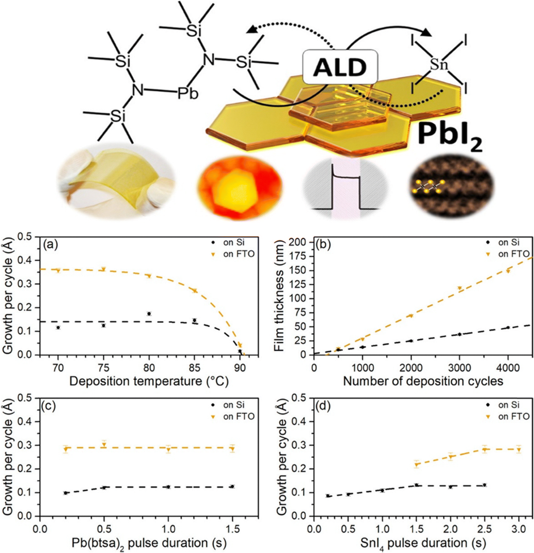 | ||
| Fig. 2 (a) Growth-per-cycle of ALD PbI2 films as a function of substrate temperature using 2000 cycles, with Pb(btsa)2 and SnI4 pulse times set to 1.0 s and 2.0 s, respectively, and 1.0 s purge steps. (b) Film thickness versus cycle number at 75 °C on Si and FTO substrates, using 1.0 s Pb(btsa)2 pulses and 2.0–2.5 s SnI4 pulses. (c) Dependence of GPC on Pb(btsa)2 pulse duration at 75 °C with fixed SnI4 dosing (2.0 s on Si, 2.5 s on FTO). (d) Dependence of GPC on SnI4 pulse duration at 75 °C with Pb(btsa)2 held at 1.0 s. Reproduced with permission from ref. 30 under the Creative Commons License (American Chemical Society). | ||
2.7. Morphology, conversion pathways, and device-level implications
Despite these limitations, ALD-derived PbI2 films have consistently demonstrated advantages in uniformity, surface smoothness, and reproducibility that remain difficult to match with solution methods. ALD produces pinhole-free films even on highly textured or porous substrates, enabling seamless integration with nanostructured electrodes, silicon-perovskite tandem architectures, and flexible electronic substrates. In several reports, perovskite crystals grown from ALD PbI2 exhibit superior film continuity and reduced thickness non-uniformity compared with spin-coated films. Vapor-phase conversion frequently yields smoother surfaces, fewer local thickness fluctuations, and reduced mechanical stress, contributing to enhanced mechanical and chemical stability under cycling, bending, or environmental exposure. These improvements are reflected in strong photoluminescence, distinct optical band-edge signatures, and reduced non-radiative pathways, although device efficiencies remain consistently below the highest reported for solution processing. Nevertheless, as perovskite devices move toward greater structural complexity and integration with silicon tandems, the ability to form uniform layers on non-planar surfaces becomes increasingly valuable, shifting the evaluation criteria beyond simple efficiency metrics.A growing body of work demonstrates that one of ALD's most distinguishing advantages, namely the ability to conformally coat extremely complex geometries, extends fully to metal-halide systems. Popov et al. reported that ALD PbCl2 deposited from Pb(btsa)2 and gallium(III) chloride (GaCl3) forms remarkably uniform shells even on deep, narrow Si trenches with an aspect ratio of roughly 1![[thin space (1/6-em)]](https://www.rsc.org/images/entities/char_2009.gif) :2:5, faithfully replicating the underlying topography without thinning, necking, or losing coverage along the sidewalls (Fig. 3). Such conformality is not simply a geometric demonstration – it directly influences the quality of subsequent perovskite formation. When organic A-site iodides diffuse into these inorganic templates during vapor conversion, a uniform halide framework facilitates more complete infiltration, reduces local stoichiometric gradients, and supports smoother crystallization across high-aspect-ratio features. As perovskite device architectures move toward deep-trench detectors, textured tandem interfaces, and buried-contact layouts where solution processing struggles to penetrate, the conformal PbCl2 shell observed in Fig. 3 illustrates why ALD halides are increasingly viewed as shape-preserving, composition-controlled scaffolds for next-generation vapor-phase perovskite growth.
:2:5, faithfully replicating the underlying topography without thinning, necking, or losing coverage along the sidewalls (Fig. 3). Such conformality is not simply a geometric demonstration – it directly influences the quality of subsequent perovskite formation. When organic A-site iodides diffuse into these inorganic templates during vapor conversion, a uniform halide framework facilitates more complete infiltration, reduces local stoichiometric gradients, and supports smoother crystallization across high-aspect-ratio features. As perovskite device architectures move toward deep-trench detectors, textured tandem interfaces, and buried-contact layouts where solution processing struggles to penetrate, the conformal PbCl2 shell observed in Fig. 3 illustrates why ALD halides are increasingly viewed as shape-preserving, composition-controlled scaffolds for next-generation vapor-phase perovskite growth.
 | ||
| Fig. 3 Cross-sectional FESEM image showing the conformal growth of an ALD PbCl2 film on patterned Si trenches. The high-aspect-ratio structures (≈1:2:5, bottom width:top width:depth) are uniformly coated along the top surfaces, sidewalls, and trench bottoms. Films were deposited at 85 °C using 600 ALD cycles with 1.5 s Pb(btsa)2 and 0.8 s GaCl3 pulses and 3 s purges. Reproduced with permission from ref. 11 under the Creative Commons Attribution 3.0 license (Royal Society of Chemistry). | ||
Additional evidence for ALD-enabled durability improvements comes from recent work showing that ALD-derived chalcogenide layers can markedly stabilize hybrid perovskites under ambient exposure. In one study, methylammonium lead iodide (MAPI) films capped with ALD lead sulfide (PbS) exhibited dramatically improved structural retention compared with uncapped controls.41 Cross-sectional SEM imaging revealed that the PbS overlayer remained dense and continuous after more than a year of storage in air (Fig. 4a), acting as a moisture-blocking barrier that preserved the underlying perovskite lattice. Grazing-incidence X-ray diffraction (GIXRD) quantified the competing evolution of PbS, PbI2, and MAPI phases as a function of the PbS deposition temperature: films grown from Pb(btsa)2 and Pb(dbda) precursors showed progressive suppression of perovskite degradation pathways when deposited near 45–65 °C (Fig. 4b and c). Stability tracking over thousands of hours demonstrated that ALD PbS caps, irrespective of precursor chemistry, maintained nearly constant MAPI reflection intensity, whereas uncapped samples rapidly lost crystallinity and underwent substantial decomposition (Fig. 4d). A mechanistic illustration further showed that elevated PbS deposition temperatures trigger premature PbI2 formation and accelerate MAPI breakdown, reinforcing the need for ultralow-temperature ALD cycles when interfacing directly with hybrid perovskites (Fig. 4e–g). All PbS overlayers were deposited by 1000 ALD cycles with 1 s precursor pulses and matched purge times. The Al2O3 film (52 nm) was deposited using 800 cycles of trimethylaluminum (TMA)/H2O at 65 °C. Taken together, these results highlight that ALD chalcogenide coatings, like ALD oxides, can function as highly effective encapsulation layers, expanding the toolbox of ALD-derived stability solutions for vapor-phase perovskite systems.
 | ||
| Fig. 4 (a) Cross-sectional SEM image of a MAPbI3 film protected with an ALD-grown PbS overlayer after prolonged ambient storage (413 days). (b) and (c) Relative reflection intensities extracted from GIXRD measurements of PbS-coated MAPbI3 films prepared using (b) Pb(btsa)2 and (c) Pb(dbda) precursors at various deposition temperatures. (d) Evolution of MAPbI3 diffraction intensities over extended air exposure for samples with no overlayer and for those capped with PbS (grown from Pb(btsa)2 or Pb(dbda)) or ALD Al2O3. (e) Illustration of film degradation processes occurring in the MAPbI3 layer when PbS ALD is performed above ∼65 °C. Reproduced with permission from ref. 41 under the Creative Commons License (American Chemical Society). | ||
2.8. A-site cation sensitivity during ALD-assisted processes
A largely under examined yet critically important dimension of ALD-based perovskite fabrication lies in the sensitivity of A-site cations to temperature, plasma exposure, and precursor chemistry. Unlike the relatively robust metal-halide sub-lattice, the organic or partially organic A-site cations, including methylammonium (MA+), formamidinium (FA+), and mixed cation systems incorporating Cs+, exhibit markedly different thermal tolerances, diffusion dynamics, and degradation pathways during vapor-phase processing.47,48 These constraints impose strict upper bounds on the process windows available for ALD growth and conversion, and they profoundly influence defect formation, lattice relaxation, and ion-migration behavior in the final perovskite structure.MA+, the most thermally fragile of the commonly used A-site species, undergoes gradual deprotonation and volatilization at temperatures above ∼100 to 120 °C, with complete decomposition typically observed near 150 °C. This decomposition is accelerated under acidic environments or in the presence of strong Lewis acids and oxidants conditions, frequently encountered during ALD reactions. As a result, MA-based perovskites are incompatible with most standard ALD chemistries unless the organic A-site incorporation occurs entirely after inorganic scaffold formation.49–51 Even during post-ALD hybrid conversion, incomplete MA+ incorporation and non-uniform cation penetration through the dense ALD-grown PbI2 can lead to heterogeneous crystal formation, spatially varying stoichiometry, and MA-deficient domains that introduce deep traps and promote phase instability.49,52–55 These challenges have contributed significantly to the field's gradual movement away from MA-rich absorbers in vapor-based methods.
FA+ offers moderately improved thermal resilience but introduces its own complexities. Its planar geometry and hydrogen-bonding interactions with the PbI6 octahedral cage render it more sensitive to lattice strain and halide coordination environments than MA+. ALD-derived PbI2 scaffolds, which often possess compact grains and limited free volume, can impede FA+ incorporation during the conversion step, leading to mixed-phase regions or partial retention of the PbI2 precursor. Moreover, FA+ is susceptible to degradation in the presence of halide radicals, residual ligands, or reactive oxygen species generated during plasma-assisted ALD cycles.56,57 These processes trigger pathways toward formamidinium iodide (HC(NH2)2I) decomposition, forming formamidine derivatives and ultimately producing nitrogen-rich byproducts. As a consequence, FA-based perovskites produced through ALD-assisted routes often show reduced grain size, higher intragrain disorder, and variations in A-site stoichiometry that complicate control over phase purity and bandgap stability.58
The introduction of Cs+ into the A-site, widely adopted to improve thermal stability and bandgap tunability, offers an important advantage for ALD compatibility: Cs-containing perovskites eliminate the thermal fragility associated with volatile organics. However, Cs+ incorporation is strongly dependent on crystallization temperature and halide mobility, both of which are tightly constrained in low-temperature ALD processes. Pure cesium lead iodide (CsPbI3), for instance, requires temperatures above ∼300 °C to stabilize the photoactive black phase, which is far above the limits of any organic-processing-compatible ALD cycle.42,59 As a result, only mixed-cation Cs-FA or Cs-MA perovskites are viable under hybrid ALD-vapor conditions, and even these systems show strong sensitivity to ALD growth density and iodination temperature. Dense ALD-grown PbI2 tends to suppress Cs+ diffusion during the conversion step, leading to compositional gradients or incomplete integration, which manifest as secondary δ-phase inclusions that degrade device performance. These challenges illustrate the inherent difficulty of reconciling the compact, highly uniform nature of ALD-grown precursors with the large-scale cation motion required for multi-cation perovskite formation.
3. Emerging low-temperature ALD strategies
The drive toward low-temperature ALD strategies for halide perovskites extends beyond any single cation or halide system and reflects a broader need to reconcile precursor reactivity with the narrow thermal tolerance of hybrid and inorganic perovskites. Approaches explored thus far include Cs-based halide chemistry, radical-assisted iodination, modified lead precursor families such as amidinates, and spatial ALD variants designed to reduce residence times. Collectively, these strategies aim to decouple reaction completeness from substrate temperature, which remains the central bottleneck in vapor-phase perovskite synthesis.Recent advances in Cs-based ALD halide chemistry further illustrate how precursor choice and temperature strongly shape the structure and morphology of vapor-grown perovskite precursors. A detailed study of ALD CsI growth (Fig. 5a–e) shows how both film continuity and crystallographic order depend sensitively on cycle number and deposition temperature. Cross-sectional field emission scanning electron microscopy (FESEM) images (Fig. 5a) reveal a clear evolution from thin, island-like layers at 400 cycles to dense, columnar films at 3300 cycles, highlighting the slow nucleation kinetics typical of low-temperature iodide ALD. Top-view images collected across different deposition temperatures (Fig. 5b) demonstrate that higher temperatures promote larger lateral grains but also increase surface porosity, an important trade-off for subsequent diffusion of Pb or organic cations during perovskite formation. GIXRD data (Fig. 5c) confirmed that CsI films crystallize readily even at 150 °C, but peak intensities and linewidths sharpen as the temperature rises, indicating improved texturing and reduced microstrain.60 AFM measurements (Fig. 5d and e) provided complementary evidence: the relative roughness decreases with increasing film thickness at low temperatures, while higher-temperature growth produces rougher but more strongly faceted surfaces. Together, these observations reinforce a broader principle emphasized throughout this review, that ALD processes for perovskite-relevant halides are governed by delicate balances between temperature, cycle count, nucleation kinetics, and surface mobility. These factors will directly influence how readily these ALD-grown CsI layers can be incorporated into all-vapor perovskite synthesis schemes or used as controlled interfaces in hybrid deposition strategies.
 | ||
| Fig. 5 Structural and morphological evolution of CsI films grown by ALD. (a) Cross-sectional FESEM images showing the transition from sparse islands (400 cycles) to a dense columnar layer (3300 cycles). (b) Top-view FESEM images of 300-cycle CsI films revealing temperature-dependent grain enlargement. (c) GIXRD patterns demonstrating enhanced crystallinity with increasing deposition temperature; reference CsI reflections (ICDD 6-311) are shown for comparison. (d) Relative AFM roughness (Rq normalized to film thickness) illustrating smoother, more compact surfaces at elevated temperatures. (e) AFM images comparing nanoscale surface textures of films grown at 150 °C and 250 °C. Reproduced with permission from ref. 42 under the Creative Commons Attribution 4.0 license (American Chemical Society). | ||
A further complication arises when attempting to form CsPbI3 through an ALD supercycle strategy. PbI2 ALD occurs only below ∼120 °C, above which common Pb precursors begin to thermally decompose, while CsI growth, in contrast, requires temperatures ≥140 °C; there is no overlap in process windows that would allow alternating CsI/PbI2 sub-cycles to co-deposit a stable CsPbI3 lattice. Earlier reactor studies have also revealed that ALD-grown PbI2 films sublimate at temperatures slightly above 100 °C, effectively eliminating the possibility of raising the substrate temperature to accommodate CsI deposition without destroying the previously formed PbI2 layer. These constraints leave only a sequential, two-step method in which a CsI layer is deposited first and then overcoated with PbI2. However, this solid–solid conversion route is sensitive to the relative amounts of each component: stoichiometric CsPbI3 forms only when CsI and PbI2 are present in the precise molar ratio required for reaction.42 PbI2 would immediately inter-diffuse into CsI during growth, and therefore, directly measuring the true PbI2 growth-per-cycle on CsI becomes impractical. To navigate this, experimental series with varied PbI2 cycle counts were performed instead, enabling observation of under-stoichiometric, over-stoichiometric, and nominally balanced conditions. X-ray diffraction analysis of these films provided direct insight into phase evolution pathways and clarified how far-from-stoichiometric depositions deviate toward Cs-rich or Pb-rich secondary phases.
Development in precursor chemistry has brought new momentum to ALD perovskite research. Improved amidinate lead precursors, with enhanced thermal stability and reduced ligand scattering cross-sections, have displayed cleaner adsorption and desorption cycles.5,29,61,62 Radical-assisted iodine activation has opened temperature windows previously inaccessible via purely thermal methods, enabling near-complete PbI2 formation at temperatures that minimize perovskite decomposition risk. Spatial ALD, with its inherently high throughput and short pulse times, has shown promise for delivering PbI2 layers that are uniform across large substrates without requiring prolonged precursor exposure.20,63–65 Meanwhile, new interest in in situ diagnostics, particularly quartz crystal microbalance (QCM) monitoring, ellipsometry, and GIXRD, have provided unprecedented insight into nucleation and halogenation kinetics, allowing researchers to rationally redesign pulsing schemes and surface activation sequences.38
4. Hybrid ALD-solution perovskite architectures
The future impact of ALD in halide perovskite research may ultimately extend beyond photovoltaic applications alone. While scalable solution and evaporation routes will likely dominate large-area module manufacturing, ALD offers unique capabilities that are particularly valuable for applications requiring conformality, deterministic thickness control, and integration with microstructured substrates. These include tandem photovoltaics, photodetectors, light-emitting diodes, and emerging perovskite-based electronic and neuromorphic devices. In such architectures, precise control over ultrathin interfaces, buried junctions, and complex topographies may justify the added process complexity associated with vapor-phase methods.66The longer-term vision for ALD perovskite growth is bold but not without precedence. If molecularly engineered precursors capable of operating near room temperature can be synthesized, direct perovskite ALD may become feasible. Such processes would transform perovskite manufacturing by enabling gradient-bandgap structures, selective area deposition, 2D/3D mixed-phase engineering, and precise compositional patterning across microstructured photonic or electronic devices.67 The adoption of spatial ALD and atmospheric-pressure ALD variants could further accelerate industrial translation by enabling high throughput and compatibility with roll-to-roll manufacturing. As the microelectronics industry has demonstrated, ALD excels when sub-nanometer precision and high surface conformity are paramount. The perovskite community now stands at a similar inflection point, exploring whether ALD's precision can be harnessed to create a new class of perovskite materials with deterministic morphological and electronic properties.
5. Outlook and conclusions
Atomic layer deposition has rapidly progressed from a supporting technology in perovskite photovoltaics into a candidate platform for deterministic, fully vapor-phase construction of halide perovskite layers. Yet, its future impact hinges on resolving several intertwined bottlenecks that arise from the chemical fragility, thermal constraints, and crystallization behavior of metal–halide perovskites. Despite substantial improvement in precursor design, halogenation strategies, and low-temperature operation, the landscape of ALD-compatible perovskite chemistries remains narrow. The limitations of existing lead precursors, whether β-diketonates, silylamides, or emerging amidinates, underline the difficulty of achieving complete ligand removal and fully saturated Pb–I frameworks below 120 °C. Any meaningful breakthrough in this area will likely come from molecularly engineered precursors with reduced ligand mass, lower activation energy for dissociation, and well-defined self-limiting behavior under halide-rich, low-temperature ALD cycles.Iodine delivery remains an equally critical impediment. HI offers unmatched reactivity but presents severe corrosion and safety concerns, while I2 and organic iodides trade chemical cleanliness for slower kinetics and incomplete halogenation at perovskite-compatible temperatures. The emergence of plasma- and radical-activated iodination approaches suggests a promising path forward: these methods can drive halogen exchange near or below 80 °C, enabling complete Pb–I bond formation without damaging the perovskite scaffold. Scaling these methods, however, will require refined control of radical flux, minimization of ion bombardment, and integration with precursor sequences capable of operating under narrow thermal windows.
A-site cation instability adds another layer of complexity. MA+ and FA+ decompose or volatilize under conditions that many ALD chemistries require, limiting direct ALD formation of hybrid ABX3 lattices and placing the burden on post-deposition vapor conversion. Even during conversion, dense ALD-grown PbI2 or CsI films can impede cation diffusion, producing non-uniform stoichiometry and phase-segregated domains. Cs-based systems offer higher thermal resilience, but their stabilization of the photoactive black phase still demands temperatures far above those accessible during ALD. These insights suggest that direct ALD growth of hybrid perovskites will require innovative precursor families that enable surface reactions at or near room temperature, an ambitious but increasingly plausible target given recent progress in ultralow-temperature ALD for other semiconductor materials.
In summary, ALD offers a suite of capabilities of sub-nanometer thickness control, perfect conformality, and unmatched interface tunability, which are profoundly relevant to the trajectory of perovskite photovoltaics and optoelectronics. Its current limitations arise mainly from precursor chemistry and temperature compatibility, rather than from intrinsic shortcomings of the ALD method itself. Continued progress in precursor design, radical-mediated halogenation, in situ diagnostics, and hybrid deposition architectures is steadily closing the gap between laboratory feasibility and practical, large-area implementation. Whether ALD ultimately becomes a primary deposition route or remains an essential auxiliary tool, it is already reshaping the scientific framework through which perovskite growth, interface engineering, and degradation pathways are understood. As the field advances toward long-term operational stability and industrial scalability, ALD will play an increasingly central role in defining how next-generation perovskite materials are engineered and deployed.
Conflicts of interest
The authors declare no competing financial interest.Data availability
No primary research results, software or code have been included.Acknowledgements
This research study was supported by the National Research Foundation of Korea (NRF) funded by the Ministry of Science and ICT (No. 2022K1A4A8A02079724) and the Korean Research Institute of Chemical Technology (KRICT), Republic of Korea (No. KS2622-20). This work was also supported by the Korean Institute of Energy Technology Evaluation and Planning (KETEP) and the Ministry of Trade, Industry & Energy (MOTIE) of the Republic of Korea (No. RS-2025-02309702).References
- S. M. George, Chem. Rev., 2010, 110, 111–131 CrossRef CAS PubMed.
- H. Hejin Park, R. Heasley and R. G. Gordon, Appl. Phys. Lett., 2013, 102, 13 CrossRef.
- J. S. Adu, G. K. Asare, B. Shin, D. J. Fermin and H. H. Park, Sol. RRL, 2025, e202500617 CrossRef CAS.
- M. Leskelä and M. Ritala, Thin Solid Films, 2002, 409, 138–146 CrossRef.
- J. Li, G. Chai and X. Wang, Int. J. Extreme Manuf., 2023, 5, 032003 CrossRef CAS.
- V. Zardetto, B. Williams, A. Perrotta, F. Di Giacomo, M. Verheijen, R. Andriessen, W. Kessels and M. Creatore, Sustainable Energy Fuels, 2017, 1, 30–55 RSC.
- X. Liao, Y. Jiang, L. Wang, J. Li, Z. Hou, K. L. Choy and Z. Li, Nanomaterials, 2025, 15, 1674 CrossRef CAS PubMed.
- M. Leskelä, M. Mattinen and M. Ritala, J. Vac. Sci. Technol., B, 2019, 37, 030801 CrossRef.
- H. H. Park and D. J. Fermin, Nanomaterials, 2023, 13, 3112 CrossRef CAS PubMed.
- J.-W. Lee, J. S. Adu, R. E. Agbenyeke, J. Laverock, A. Sheppard, E. Park, Y. Kim, S. Hong, N. J. Jeon, D. J. Fermin and H. H. Park, J. Mater. Chem. A, 2025, 13, 4100–4106 RSC.
- G. Popov, G. Bačić, C. Van Dijck, L. S. Junkers, A. Weiß, M. Mattinen, A. Vihervaara, M. Chundak, P. Jalkanen, K. Mizohata, M. Leskelä, J. D. Masuda, S. T. Barry, M. Ritala and M. Kemell, Dalton Trans., 2022, 51, 15142–15157 RSC.
- V. Miikkulainen, M. Leskelä, M. Ritala and R. L. Puurunen, J. Appl. Phys., 2013, 113, 021301 CrossRef.
- Y. S. Lee, T. Gershon, T. K. Todorov, W. Wang, M. T. Winkler, M. Hopstaken, O. Gunawan and J. Kim, Adv. Energy Mater., 2016, 6, 1600198 CrossRef.
- H. Jung, G. Kim, G. S. Jang, J. Lim, M. Kim, C. S. Moon, X. Hao, N. J. Jeon, J. S. Yun, H. H. Park and J. Seo, ACS Appl. Mater. Interfaces, 2021, 13, 30497–30503 CrossRef CAS PubMed.
- T. Eom, S. Kim, R. E. Agbenyeke, H. Jung, S. M. Shin, Y. K. Lee, C. G. Kim, T.-M. Chung, N. J. Jeon, H. H. Park and J. Seo, Adv. Mater. Interfaces, 2021, 8, 2001482 CrossRef CAS.
- H. H. Park, T. J. Larrabee, L. B. Ruppalt, J. C. Culbertson and S. M. Prokes, ACS Omega, 2017, 2, 1259–1264 CrossRef CAS PubMed.
- H. H. Park, Nanomaterials, 2022, 12, 4326 CrossRef CAS PubMed.
- J. S. Adu, A. Sheppard, R. E. Agbenyeke, G. K. Asare, B. H. Hamadani, D. J. Fermin and H. H. Park, Small, 2025, 2412702 CrossRef CAS PubMed.
- H. H. Park, S. Song and J. Seo, Mater. Today Energy, 2021, 21, 100729 CrossRef.
- H. Asgarimoghaddam, Q. Chen, F. Ye, A. Shahin, B. Song and K. P. Musselman, Small Methods, 2024, 8, 2300995 CrossRef CAS PubMed.
- G. K. Asare, J. S. Adu, B. Shin, D. J. Fermin and H. H. Park, Electron. Mater. Lett., 2025, 21, 331–336 CrossRef CAS.
- E. Choi, J. W. Lee, M. Anaya, A. Mirabelli, H. Shim, J. Strzalka, J. Lim, S. Yun, M. Dubajic, J. Lim, J. Seidel, R. E. Agbenyeke, C. G. Kim, N. J. Jeon, A. M. Soufiani, H. H. Park and J. S. Yun, Adv. Energy Mater., 2023, 13, 2301717 CrossRef CAS.
- D. Koushik, W. J. H. Verhees, Y. Kuang, S. Veenstra, D. Zhang, M. A. Verheijen, M. Creatore and R. E. I. Schropp, Energy Environ. Sci., 2017, 10, 91–100 RSC.
- R. Zhao, K. Zhang, J. Zhu, S. Xiao, W. Xiong, J. Wang, T. Liu, G. Xing, K. Wang, S. Yang and X. Wang, Nanoscale Adv., 2021, 3, 2305–2315 RSC.
- M. Kot, K. Henkel, K. Müller, L. Kegelmann, S. Albrecht, N. Tsud, P. Kús, I. Matolinová and D. Schmeißer, Energy Technol., 2019, 7, 1900975 CrossRef CAS.
- H. H. Park, A. Jayaraman, R. Heasley, C. Yang, L. Hartle, R. Mankad, R. Haight, D. B. Mitzi, O. Gunawan and R. G. Gordon, Appl. Phys. Lett., 2014, 105, 202101 CrossRef.
- V. Zardetto, B. L. Williams, A. Perrotta, F. Di Giacomo, M. A. Verheijen, R. Andriessen, W. M. M. Kessels and M. Creatore, Sustainable Energy Fuels, 2017, 1, 30–55 RSC.
- B. R. Sutherland, S. Hoogland, M. M. Adachi, P. Kanjanaboos, C. T. O. Wong, J. J. McDowell, J. Xu, O. Voznyy, Z. Ning, A. J. Houtepen and E. H. Sargent, Adv. Mater., 2015, 27, 53–58 CrossRef CAS PubMed.
- P. Kaur, L. Mai, A. Muriqi, D. Zanders, R. Ghiyasi, M. Safdar, N. Boysen, M. Winter, M. Nolan and M. Karppinen, Chem. – Eur. J., 2021, 27, 4913–4926 CrossRef CAS PubMed.
- G. Popov, M. Mattinen, T. Hatanpää, M. Vehkamäki, M. Kemell, K. Mizohata, J. Räisänen, M. Ritala and M. Leskelä, Chem. Mater., 2019, 31, 1101–1109 CrossRef CAS.
- J. N. Vagott, K. Bairley, J. Hidalgo, C. A. Perini, A.-F. Castro-Méndez, S. Lombardo, B. Lai, L. Zhang, K. Kisslinger and J. Kacher, Chem. Mater., 2022, 34, 2553–2561 CrossRef CAS.
- H. Sun, X. Zhu, D. Yang, J. Yang, X. Gao and X. Li, J. Cryst. Growth, 2014, 405, 29–34 CrossRef CAS.
- V. Held, N. Mrkyvkova, P. Nadazdy, K. Vegso, A. Vlk, M. Ledinsky, M. Jergel, A. Chumakov, S. V. Roth and F. Schreiber, J. Phys. Chem. Lett., 2022, 13, 11905–11912 CrossRef CAS PubMed.
- N. M. Sbrockey, G. S. Tompa, R. Lavelle, K. A. Trumbull, M. A. Fanton, D. W. Snyder, R. G. Polcawich and D. M. Potrepka, J. Vac. Sci. Technol., A, 2018, 36, 031509 CrossRef.
- M. Weber, N. Boysen, O. Graniel, A. Sekkat, C. Dussarrat, P. Wiff, A. Devi and D. Muñoz-Rojas, ACS Mater. Au, 2023, 3, 274–298 CrossRef CAS PubMed.
- J. Harjuoja, M. Putkonen and L. Niinistö, Thin Solid Films, 2006, 497, 77–82 CrossRef CAS.
- J. Harjuoja, S. Väyrynen, M. Putkonen, L. Niinistö and E. Rauhala, Appl. Surf. Sci., 2007, 253, 5228–5232 CrossRef CAS.
- A. E. Bracesco, J. W. P. Jansen, H. Xue, V. Zardetto, G. Brocks, W. M. Kessels, S. Tao and M. Creatore, ACS Appl. Mater. Interfaces, 2023, 15, 38018–38028 CrossRef CAS PubMed.
- A. Weiß, M. Terletskaia, G. Popov, K. Mizohata, M. Leskela, M. Ritala and M. Kemell, Chem. Mater., 2023, 35, 8722–8732 CrossRef.
- J. Haeberle, K. Henkel, H. Gargouri, F. Naumann, B. Gruska, M. Arens, M. Tallarida and D. Schmeißer, Beilstein J. Nanotechnol., 2013, 4, 732–742 CrossRef CAS PubMed.
- G. Popov, G. Bačić, M. Mattinen, T. Manner, H. Lindström, H. Seppänen, S. Suihkonen, M. Vehkamäki, M. Kemell, P. Jalkanen, K. Mizohata, J. Räisänen, M. Leskelä, H. M. Koivula, S. T. Barry and M. Ritala, Chem. Mater., 2020, 32, 8216–8228 CrossRef CAS.
- A. Weiß, G. Popov, E. Atosuo, A. Vihervaara, P. Jalkanen, M. Vehkamaki, M. Leskela, M. Ritala and M. Kemell, Chem. Mater., 2022, 34, 6087–6097 CrossRef.
- H. B. Profijt, S. E. Potts, M. C. M. van de Sanden and W. M. M. Kessels, J. Vac. Sci. Technol., A, 2011, 29, 050801 CrossRef.
- R. Zhao, K. Zhang, J. Zhu, S. Xiao, W. Xiong, J. Wang, T. Liu, G. Xing, K. Wang and S. Yang, Nanoscale Adv., 2021, 3, 2305–2315 RSC.
- P. Poodt, A. Lankhorst, F. Roozeboom, K. Spee, D. Maas and A. Vermeer, Adv. Mater., 2010, 22, 3564–3567 CrossRef CAS PubMed.
- G. A. Somorjai and Y. Li, Introduction to Surface Chemistry and Catalysis, Wiley, New York, 1994 Search PubMed.
- N. Li, Y. Luo, Z. Chen, X. Niu, X. Zhang, J. Lu, R. Kumar, J. Jiang, H. Liu, X. Guo, B. Lai, G. Brocks, Q. Chen, S. Tao, D. P. Fenning and H. Zhou, Joule, 2020, 4, 1743–1758 CrossRef CAS.
- Y. Li, Z. Chen, B. Yu, S. Tan, Y. Cui, H. Wu, Y. Luo, J. Shi, D. Li and Q. Meng, Joule, 2022, 6, 676–689 CrossRef CAS.
- K. Zhao, L. Yao, C. Değer, X. Zhang, J. Shen, X. Miao, P. Shi, Y. Luo, D. Jin and Y. Tian, Nat. Commun., 2025, 16, 10074 CrossRef CAS PubMed.
- L. Ma, D. Guo, M. Li, C. Wang, Z. Zhou, X. Zhao, F. Zhang, Z. Ao and Z. Nie, Chem. Mater., 2019, 31, 8515–8522 CrossRef CAS.
- T. T. Ava, A. Al Mamun, S. Marsillac and G. Namkoong, Appl. Sci., 2019, 9, 188 CrossRef CAS.
- Z. Song, S. C. Watthage, A. B. Phillips, B. L. Tompkins, R. J. Ellingson and M. J. Heben, Chem. Mater., 2015, 27, 4612–4619 CrossRef CAS.
- E. J. Juarez-Perez, L. K. Ono, M. Maeda, Y. Jiang, Z. Hawash and Y. Qi, J. Mater. Chem. A, 2018, 6, 9604–9612 RSC.
- S. Thankaraj Salammal, V. Panneerselvam, K. K. Chinnakutti, P. Manidurai and K. Parasuraman, J. Vac. Sci. Technol., A, 2021, 39, 022801 CrossRef CAS.
- L. Qiu, S. He, Y. Jiang and Y. Qi, J. Mater. Chem. A, 2021, 9, 22759–22780 RSC.
- B. Kammlander, S. Svanström, D. Kühn, F. O. Johansson, S. Sinha, H. Rensmo, A. G. Fernández and U. B. Cappel, Chem. Commun., 2022, 58, 13523–13526 RSC.
- J. Hidalgo, W. Kaiser, Y. An, R. Li, Z. Oh, A.-F. Castro-Méndez, D. K. LaFollette, S. Kim, B. Lai, J. Breternitz, S. Schorr, C. A. R. Perini, E. Mosconi, F. De Angelis and J.-P. Correa-Baena, J. Am. Chem. Soc., 2023, 145, 24549–24557 CAS.
- T. Burwig, K. Heinze and P. Pistor, Phys. Rev. Mater., 2022, 6, 065404 CrossRef CAS.
- S. Ma, S. H. Kim, B. Jeong, H. C. Kwon, S. C. Yun, G. Jang, H. Yang, C. Park, D. Lee and J. Moon, Small, 2019, 15, 1900219 CrossRef PubMed.
- T. W. Jones, A. Osherov, M. Alsari, M. Sponseller, B. C. Duck, Y.-K. Jung, C. Settens, F. Niroui, R. Brenes and C. V. Stan, Energy Environ. Sci., 2019, 12, 596–606 RSC.
- A. L. Johnson and J. D. Parish, in Organometallic Chemistry, ed. N. J. Patmore and P. I. P. Elliott, The Royal Society of Chemistry, 2018, vol. 42 Search PubMed.
- R. Ji, A. Mallick, B. Rivkin, H. Yuce-Cakir, O. D. Jurchescu and Y. Vaynzof, Adv. Mater., 2025, 37, 2416604 CrossRef CAS PubMed.
- L. Hoffmann, K. O. Brinkmann, J. Malerczyk, D. Rogalla, T. Becker, D. Theirich, I. Shutsko, P. Görrn and T. Riedl, ACS Appl. Mater. Interfaces, 2018, 10, 6006–6013 CrossRef CAS PubMed.
- R. L. Z. Hoye, D. Muñoz-Rojas, Z. Sun, H. Okcu, H. Asgarimoghaddam, J. L. MacManus-Driscoll and K. P. Musselman, PRX Energy, 2025, 4, 017002 CrossRef.
- X. Jiang, B. Shan, G. Ma, Y. Xu, X. Yang, W. Zhou, C. Li, F. Yang and R. Chen, Chem. Eng. J., 2025, 505, 159629 CrossRef CAS.
- D. Koushik, L. Hazendonk, V. Zardetto, V. Vandalon, M. A. Verheijen, W. M. Kessels and M. Creatore, ACS Appl. Mater. Interfaces, 2019, 11, 5526–5535 CrossRef CAS PubMed.
- J. Gong, M. Song, Y.-K. Kim and G. M. Kim, Adv. Ind. Eng. Chem., 2025, 1, 10 CrossRef.
| This journal is © The Royal Society of Chemistry 2026 |