
 Open Access Article
 This Open Access Article is licensed under a
 Creative Commons Attribution 3.0 Unported Licence
Dilute anion alloyed III-nitride nanowires for photoelectrochemical water splitting†
S. J.
Calero-Barney
a,
A. C.
Nouduri
a,
A. N.
Andriotis
b,
M.
Menon
a and
M. K.
Sunkara
 *a
*a
aConn Center for Renewable Energy Research, University of Louisville, Louisville, Kentucky 40292, USA. E-mail: mahendra@louisville.edu
bInstitute of Electronic Structure and Laser, FORTH, P.O. Box 1527, 71110 Herakilo, Crete, Greece
First published on 2nd April 2025
Abstract
Dilute anion alloyed III-nitride nanowires exhibited band gap reduction to around 2.4 eV with anion concentrations ranging from 5.6 to 8.8 at% and exhibited photoelectrochemical activity (∼8 mA cm−2@10 sun) under AM1.5 visible light. The nanowire electrode also exhibited photoelectrochemical activity using 470 nm wavelength light up to 8.75 mA cm−2 at 10 sun (470 nm) radiation. The nanowires are grown using a plasma assisted vapor liquid solid (PA-VLS) technique using N2 gas. The anion-alloyed antimony alloyed gallium nitride (GaSbxN1−x) and bismuth alloyed gallium nitride (GaBiyN1−y) wurtzite nanowires were grown using PA-VLS employing gold and copper as metallic seeds on a variety of substrates such as silicon, sapphire, and stainless steel. The PA-VLS technique allowed for increasing the antimony and bismuth incorporation levels with temperature as the dissolution of these species into the metals was favored with growth temperatures. Photoelectrochemical spectroscopy measurements showed light absorption of 620 nm photons in the case of the GaSb0.056N0.944 sample.
1. Introduction
Single crystalline III–V materials exhibit excellent opto-electronic properties and exhibit tuneable band gaps and band edges with alloying. There has been significant progress in the growth of cation alloyed (III1−xIIIxV) materials, i.e., GaInP, GaInAs, AlGaAs, and AlGaP.1 However, the band edges of these materials do not straddle hydrogen and oxygen evolution reaction potentials when the band gaps are reduced to around 2 eV. Nanowires of GaAsSb, InAsSb, InAsP and GaAsP have been synthesized through selective area vapor–solid,2–7 or catalysed vapor–liquid–solid8–12 mechanisms using metal organic vapor phase epitaxy (MOVPE), metalorganic chemical vapor deposition (MOCVD) and/or molecular beam epitaxy (MBE) techniques. The proposed applications for the above anion diluted alloys revolved around transistors and infrared sensors.GaN has a band gap of 3.45 eV with its band edges straddling both hydrogen and oxygen evolution reactions. So, alloying of GaN has received much interest in producing semiconductors with band gaps in the visible range. Cationic alloying of GaN has received significant interest. For example, InGaN films in particular have shown continuous band gap reduction, reaching values of 2.7 to 2.1 eV with In incorporation between 30 and 50 mol%, respectively13 or In mol% ≫ 20.14 Anion alloying of GaN was predicted and proposed to produce visible light absorbing semiconductors with appropriate band edges for unassisted water splitting.15
The synthesis of dilute anion alloys of III-nitrides through MOCVD and MBE has always been a challenge because of the low decomposition and evaporation temperatures of GaN and group-III elements, respectively,16 which contrast with the high temperatures required for ammonia cracking. Additionally, this precursor accounts for 30–50% of MOCVD costs17 due to its low incorporation efficiency (3.8% at 700 °C).16 To circumvent these challenges many works on binary GaN and AlN systems introduced the use of nitrogen plasma, enabling the growth at lower temperatures compared to ammonia sourced MBE and MOCVD.18 Plasma-assisted techniques have also made possible the growth of In-containing nitrides, otherwise limited by InN low sublimation temperature at moderate pressures.19
Lower growth temperatures in plasma-assisted vapor–solid growth techniques have also served to overcome challenges in the synthesis of IIIV1−xVx nitrides that suffer from low anion substitution, due to the high vapor pressures of group-V elements. Using low temperature MOCVD, the concept of dilute anion alloying into GaN was studied and showed that drastic band gap reduction to around 2 eV can be obtained with Sb alloying of GaN with modest amounts, which also exhibited band edges straddling OER and HER potentials.20 Through plasma assisted molecular beam epitaxy (PA-MBE), a 1.2 eV band gap GaBi0.11N0.89 was achieved.21 Other studies of alloys with visible light absorption behaviour such as PA-MBE-grown GaSbN confirm a drastic band gap shift from 3.4 to 2 eV with antimony content below 5 mol%,22 and 1 mol%.23 In contrast, in our own experimental work on plasma assisted vapor liquid phase epitaxy (PA-VLPE) synthesis of GaSbN and GaBiN films, we did not observe a band gap reduction (versus pure GaN) for alloys with antimony or bismuth content less than 1 at%, and DFT simulations suggest that GaN band gap reduction can only be achieved when the antimony content is between 2 and 3 at%.24 Other studies of our group with ammonia sourced20 and plasma-assisted25 MOCVD have enabled the growth of polycrystalline GaSbN films (2–8 Sb at%). In addition, nanowires containing 2–4 Sb at% have been grown using ammonia in a MOCVD reactor with copper as catalyst that exhibited band gaps around 2 eV. However, the photoelectrochemical activity was limited.
In the present work, we present the results of Au and Cu catalysed PA-VLPE synthesis of GaSbxN1−x and GaBiyN1−y nanowires where x and y lie between 3.4 and 5.6 at% and 1 and 8.8 at%, respectively. Most importantly, the resulting nanowires were studied to understand photo-electrochemical activity as a function of wavelength.
2. Experimental methods
2.1 Material synthesis
Sapphire substrates coated with a catalyst layer (gold or copper) are loaded into the quartz tube that is heated with a one-zone furnace. Gallium and group-V metals (antimony or bismuth) are loaded in quartz boats and kept them before the substrates. Radio frequency plasma is generated right after the furnace.After the substrates and precursors are loaded in the appropriate positions inside the tube, the system is closed, purged with hydrogen, and leak checked. To remove any oxide from the substrates and metallic precursors, 50 sccm of hydrogen are fed into the system and 70 W are applied to the flowing gas while the system is heated from room temperature to 750 °C, which takes about 15 min. While keeping the furnace temperature at 750 °C, 10 sccm of hydrogen chloride diluted in 50 sccm of hydrogen are fed for one hour, to transport gallium and group-V halide species that result from the reaction between hydrogen chloride and the metals. Since the substrates have a 20 nm catalyst coating, the flux of GaCl and SbCl/BiCl reached the surface, and the species dissolved into the catalyst.
After the “transport” step has been completed, the furnace temperature is raised to the growth temperature (between 800 and 950 °C) and a mixture of 40 sccm of nitrogen, 15 sccm of argon and 10 sccm of HCl are fed into the system. As has been explained elsewhere,13 N2 gas does not react with gallium to form GaN at the pressure and temperature conditions used in this study, and therefore 70 W radio frequency power was applied intermittently (0.5 min on and 5 min off) to the gas mixture for one hour, generating ionized and other activated nitrogen species that dissolved into the catalyst and formed the alloys by reacting with gallium and antimony/bismuth. It is worth noting that high (Ga + Sb/Bi)/N ratio was likely the prevalent condition in all experiments, given that gallium and antimony/bismuth fluxes are exponentially proportional to temperature, as the metals react with hydrogen chloride during “transport” and “growth” steps at 750 °C and 800–950 °C, respectively, while nitridation occurs only during the “growth” step.
2.2 Electrochemical measurements
The electrochemical measurements were performed in a 3-electrode configuration (unless stated otherwise), using a platinum counter electrode, a Ag/AgCl reference electrode, and a Ga(Sb/Bi)xN1−x working electrode. The electrochemical cell had a capacity of 100 mL and was equipped with a quartz window. A 0.5 M sulfuric acid solution was the electrolyte used to conduct baseline measurements, and a mixture of 0.5 M and 1 mM sulfuric acid and sodium sulfite was used to evaluate the alloy's photo-electrochemical performance without charge transfer limitations at the alloy–electrolyte interface. A Newport solar simulator was used on its own or coupled with a monochromator for the photocurrent spectroscopy measurements. A 470 nm LED was also used for some of the photoelectrochemical measurements. The reported irradiance values of the different light sources were measured using a calibrated photodiode purchased from Thorlabs.3. Results and discussion
Scanning electron micrographs of GaSbxN1−x and GaBiyN1−y nanowires grown at different temperatures are shown in Fig. 1. The growth temperature affects both the alloying degree and the shape of the wires, i.e., at 800 °C GaSbxN1−x wires are very thin, and the antimony incorporation is only 3.4%; however, the wire diameters become larger at 900 °C and 950 °C and the antimony content in these alloys is 4.9 and 5.6 at%, respectively. A similar trend can be observed in GaBiyN1−y samples, where thin wires with low bismuth content are obtained at 800 °C, and the wire diameter increases as well as the bismuth content when the growth temperature was increased to 950 °C. The diffusion coefficient of all alloy constituents into the catalyst increases with temperature and so does the (Ga + Sb/Bi)/N ratio (as explained in the ESI†) which promotes the morphological changes observed, as has been described26 where they studied GaN wire growth through halide VLS mechanism, that an increase in the GaCl flux while keeping ammonia flux constant, would favour lateral growth over axial growth resulting in shorter and thicker wires. | ||
| Fig. 1 GaSbxN1−x wires grown at (a) 800 °C, (b) 900 °C and (c) 950 °C. GaBiyN1−y wires grown at (d) 900 °C and (e) 950 °C. | ||
Fig. 2a shows the GaSb0.041N0.959 sample grown at 850 °C, the wire growth direction was identified as the a-plane because it was parallel to the 10![[1 with combining macron]](https://www.rsc.org/images/entities/char_0031_0304.gif) 0 direction. The corresponding hexagonal diffraction pattern is shown in Fig. 2b and high-resolution transmission electron micrographs perpendicular to the wire's c-plane orientation are shown in Fig. 2c and d. The interplanar distance, for 100, 010 and 100 was determined to be 2.69, 2.83 and 2.69 Å, respectively, averaging 2.74 Å which is close to pure an-GaN interplanar distance of 2.76 Å. Considering that the wires are mostly exposing c-plane when still attached to the substrate (see Fig. 1), it is consistent to observe (002) peak in the X-ray diffraction measurements (Fig. 3). The growth direction for nanowires is important as it can have drastic effect on defects along the growth direction and conductivity.27
0 direction. The corresponding hexagonal diffraction pattern is shown in Fig. 2b and high-resolution transmission electron micrographs perpendicular to the wire's c-plane orientation are shown in Fig. 2c and d. The interplanar distance, for 100, 010 and 100 was determined to be 2.69, 2.83 and 2.69 Å, respectively, averaging 2.74 Å which is close to pure an-GaN interplanar distance of 2.76 Å. Considering that the wires are mostly exposing c-plane when still attached to the substrate (see Fig. 1), it is consistent to observe (002) peak in the X-ray diffraction measurements (Fig. 3). The growth direction for nanowires is important as it can have drastic effect on defects along the growth direction and conductivity.27
 | ||
| Fig. 2 (a) GaSb0.041N0.959 wire grown at 850 °C showing a-plane orientation, (b) its corresponding diffraction pattern, (c) and (d) high-resolution transmission electron micrographs of the wire's c-plane orientation. | ||
 | ||
| Fig. 3 X-ray diffraction measurements of (a) GaSbxN1−x and (b) GaBiyN1−y samples with different degrees of alloying. Tauc plots of (c) GaSbxN1−x and (d) GaBiyN1−y samples with different degrees of alloying. | ||
XRD data in Fig. 3a and b clearly indicate the alloying of Sb and Bi into GaN as shown by shift of (002) peak to lower values indicating lattice expansion with alloying. Based on the peak shift, the estimated degree of alloying (x or y) increases as a function of temperature from 3.4 to 5.6 at% in the case of GaSbxN1−x wires, and from 1 to 8.8 at% in the case of GaBiyN1−y alloys grown between 800 °C and 950 °C, respectively. Higher growth temperatures result in larger (002) peak shifts towards lower 2θ values with respect to pure GaN. As described previously, the (Ga + Sb)/N ratio increases as a function of temperature, and therefore, the availability and incorporation of substitutional species increases as well. The solubility of alloying element in molten catalyst cluster increases with growth temperature leading to higher incorporation during nanowire growth.
Fig. S1 of the ESI† shows a transmission electron micrograph of GaSbxN1−x wires grown at 850 °C and the corresponding elemental mapping. Fig. S1a (ESI†) shows a high-resolution transmission electron micrograph where a round darker element stands out, and the contrast difference suggests it probably contains a high conductivity element. Being located at the tip of the wire is indicative of a vapor liquid solid mechanism of alloy growth by dissolution into copper droplets. In Fig. S1c of the ESI,† it can be observed that copper mainly concentrates in round areas, and even though the alloyed nature of the samples has been discussed previously, antimony seems to have a higher concentration in the same spots as copper (see Fig. S1e of the ESI†).
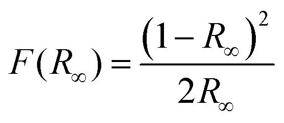
Fig. 3c and d show Tauc plots of GaSbxN1−x and GaBiyN1−y samples with different degrees of alloying. These plots were derived from diffuse reflectance measurements carried out using a PerkinElmer Lambda 950 spectrometer equipped with a 60 mm integrating sphere. The spectral absorption coefficients were estimated using the Kubelka–Munk function with the following expression:
All the samples are grown on a GaN-coated substrate. GaBiyN1−y samples with 1.0 and 2.6 at% of bismuth show a direct absorption band edge close to 3.4 eV that corresponds to pure GaN. The alloy with a bismuth content of 8.8 at% has a very sharp absorption edge at ∼2.5 eV, which was not observed for the lower alloying of Bi. The growth of the alloys on these substrates is porous, and the absorption band at 3.4 eV is indicative of this coating. GaSbxN1−x samples with 4.9 and 5.6 degrees of alloying have a sharper absorption edge at 2.3–2.45 eV. These samples also have the characteristic absorption band at 3.4 eV for the GaN coating.
The estimated bandgap values of GaSbxN1−x alloys agree with results obtained through DFT calculations reported in previous studies.24 For the case of GaBiyN1−y, the structural optimization and electronic structure analysis for all Bi doped GaN structures were performed using first principles density functional theory (DFT). The DFT calculations are performed in the generalized gradient approximation (GGA) of Perdew–Burke–Ernzerhof (PBE)28 for exchange and correlation and augmented by including Hubbard-U corrections29 based on Dudarev's approach30 as implemented in the Vienna ab initio simulation package (VASP).31–33 The projected augmented wave (PAW) potential32,33 is used to describe the core electrons. The Hubbard-U parameter is applied as a many-body correction to overcome the underestimation of electronic correlation due to the approximate nature of the exchange–correlation functionals in the traditional single-particle Kohn–Sham DFT. It partially corrects the electronic self-interaction error inherent in DFT and leads to better gap estimations. The U parameter is an on-site Coulomb repulsion parameter that incorporates part of the electron correlation absent in LDA/GGA. The U values used in the GGA+U formalism are: Ud(Ga) = 6.5 eV and Up(N) = Up(Bi) = −4.2 eV. All other U values such as Up(Ga), Us(Ga), Us(N), and Us(Bi) are set to zero. These values of U for Ga and N reproduce the experimental band gap of bulk GaN (3.43 eV).33 The bulk GaN in the wurtzite structure was simulated using a 192-atom supercell with periodic boundary conditions. GaBiyN1−y structures are obtained by substituting up to 6 N atoms with Bi. After testing for convergence, we settled for a 3 × 6 × 2 Γ-centered pack for k-vector sampling. A kinetic energy cutoff of 550 eV was found to be sufficient to achieve a total energy convergence of the energies of the systems to within 1 meV. Gaussian smearing of 0.05 eV was chosen to accelerate the electronic convergence. The optimization of atomic positions (including full cell optimization) was allowed to proceed without any symmetry constraints until the force on each atom was less than 5 meV A−1. In each case considered, both the cell volume and the individual atomic positions have been fully optimized without any symmetry constraints.
Our calculations for GaBiyN1−y structures reveal a monotonic increase in the lattice parameters with an increase in y on electronegativity mismatch between N and Bi. Fig. S2 (ESI†) shows the optimized atomic configuration for the GaN supercell with 4 substitutional Bi.
The electronic structure analysis shows a rapid initial decrease in the band gap with an increase in the dopant concentration for the GaBiyN1−y system. Pristine GaN is a wide band gap material with a fundamental band gap of ∼3.4 eV. The introduction of the first substitutional Bi produces a localized state just above the valence band maximum (VBM) of GaN. The addition of more substitutional Bi atoms broadens and delocalizes this state. This explains the rapid initial decrease and subsequent slow variation of the band gap seen in Fig. S3 (ESI†), which shows the calculated electronic band gaps as a function of the fraction, y, for GaBiyN1−y. In all cases considered, the gaps are direct. As seen in Fig. S4 (ESI†), there are several strongly hybridized states of Ga-p, N-s, N-p, and Bi-p character that contribute to the band edge states. In particular, the conduction band minimum (CBM) is a hybrid state composed of the p orbital of a Ga atom nearest neighbour to Bi and the s state of an N atom bonded to this Ga atom. The VBM, on the other hand, is dominated by the Bi-p states.
Photocurrent spectroscopy measurements were carried out with GaSbxN1−x samples containing 4.1 and 5.6 at% of antimony and GaN (GaSb0.041N0.959 and GaSb0.056N0.944, respectively) samples. Electrodes were made using 1 cm2 area samples with InGa eutectic spread on top before attaching the copper wire with silver epoxy. These measurements were carried out using a Newport solar simulator set for an irradiance of 10 sun (1000 mW cm−2), in conjunction with a monochromator that was manually set at each wavelength from 320 nm to the photoactivity limit of each sample, with increments of 5 and 10 nm for the alloy samples and GaN sample respectively. The photocurrent was measured under 0.5 V vs. RHE. The results are presented in Fig. 4. GaSb0.056N0.944 and GaSb0.041N0.959 samples exhibit photocurrents up to 620 nm (2.00 eV) and 585 nm (2.12 eV), respectively, while pure GaN is not photoactive beyond 370 nm (or below 3.35 eV). It is worth noting that the photocurrent values at the starting wavelength of 320 nm are low, then increase at 340 nm, and then decrease again until the absorption cutoff is reached. This is due to the difficulty of controlling the photon irradiance after the light beam is filtered in the monochromator. See Fig. S7 of light intensity vs. wavelength in the ESI,† where the lamp intensity decreases at higher wavelengths as seen in the ESI.†
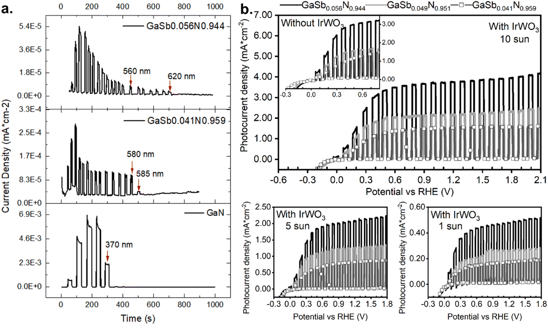 | ||
| Fig. 4 (a) Photocurrent spectroscopy measurements of GaSb0.056N0.944 and GaSb0.041N0.959 samples. (b) Photocurrent density versus applied bias in 3-electrode configuration of Ir0.02W1−0.98O3−δ decorated samples GaSb0.041N0.959, GaSb0.049N0.951 and GaSb0.056N0.944, under 1, 5 and 10 sun irradiance. Performance of same three samples under 10 sun irradiance without Ir0.02W1−0.98O3−δ (inset). | ||
Photocurrent spectroscopy measurements tend to overestimate the absorption cutoff versus the optical band gap of materials because a portion of the photo-generated carriers recombines before they can be measured as current. Nonetheless, the photocurrent spectroscopy measurements of three alloys shown in Fig. 4a are in good agreement with the optical band gap values deduced from Tauc plots.
Linear sweep voltammetries of IrxWO3−x decorated samples GaSb0.041N0.959, GaSb0.049N0.951 and GaSb0.056N0.944, under 1, 5 and 10 sun irradiance are shown in Fig. 4b. The measurements were conducted in a three-electrode configuration using Ag/AgCl and platinum mesh as reference and counter electrodes, respectively. The photocurrent onset is visible at applied biases that differ among the samples within tens of mV around 0 V vs. RHE. Surprisingly, the same photocurrent density onset potential was observed for the uncatalyzed samples (see inset in Fig. 4b), but the fill factor was improved. Overall, the use of the catalyst was to improve the fill factor and intensity near onset potentials. More details about the synthesis of IrxW1−xO3−δ can be found in the work by Kumari et al.34 Ir0.02W0.98O3−x loading in this study was approximately 0.028 mg cm−2. With using the electrocatalyst, one can clearly see that the on-set potentials are slightly negative to 0 vs. RHE, suggesting the band edges straddle both hydrogen and oxygen evolution reactions for the alloys with band gaps around 1.9–2.0 eV. The data in Fig. 4b show the performance of three samples with compositions in the similar range and yet exhibited different photoelectrochemical performance. The samples were grown in different experiments and exhibit different amounts of nanowire film thicknesses, resulting in different amounts of light absorption.
As expected, the increase of irradiance has a positive effect on the magnitude of the photocurrent density, i.e., Jph at 5 sun is approximately 5 × (Jph at 1 sun); however, the photocurrent density at 10 sun falls short of the expected proportional increase. Based on the overall results, increasing activity with increasing intensity suggests that the photoactivity of the alloys might be absorption limited.
Photocurrent density magnitude is also impacted by antimony incorporation differences among the three samples shown in Fig. 5a–c, which compares the photocurrent density versus applied bias of each sample under 10 sun illumination of full spectrum or 10 sun of 470 nm LED. Considering photocurrent spectroscopy, Tauc plots, and absorption coefficient results, it is reasonable to assume that photocurrent density under 470 nm illumination should be twice as high compared to when a full spectrum source is used. That is the case for the sample GaSb0.056N0.944. The GaSb0.049N0.951 sample only shows a 1.5 times increase, but the sample GaSb0.041N0.959, which has the lowest absorption coefficient, shows an increase of photocurrent density of 2.5 times. GaSb0.041N0.959 samples are also the ones with thinnest and less vertically aligned wires, which can explain why 470 nm photons can be efficiently absorbed while photons with a broad wavelength distribution cannot. Optical absorption coefficients versus photon energy (see Fig. 5d) show low absorption of photons with energies below 1.8 eV, which means only about half of the energy input supplied with full-spectrum illumination can be absorbed by these alloys. The GaSb0.041N0.959 sample exhibits the lowest absorption coefficient, but it increases towards the visible range, while GaSb0.049N0.951 and GaSb0.056N0.944 samples have similar absorption capability with weaker wavelength dependence.
 | ||
| Fig. 5 Photocurrent density versus applied bias in 3-electrode configuration, under 10 sun irradiance of full spectrum (grey lines) or 470 nm (black lines). (a) GaSb0.041N0.959, (b) GaSb0.049N0.951 and (c) GaSb0.056N0.944. (d) Optical absorption coefficient versus photon energy of same three samples (solid lines) and x10(AM 1.5 G) irradiance versus photon energy (dotted line). (e) Photocurrent density versus time of sample GaSb0.056N0.944 in a 2-electrode configuration (p-Si counter electrode), at 0.5 V vs. p-Si and 10 sun/470 nm illumination. | ||
Fig. 5e shows the photocurrent density of sample GaSb0.056N0.944 shorted with a p-Si electrode under 0.5 V and 10 sun/470 nm illumination. The power is calibrated using Si photodiode with intensity as equivalent to that of 10 suns. The intensity is 1 W cm−2. The photocurrent magnitude was high enough to produce visible hydrogen and oxygen bubble formation at the surface of the electrodes. The photocurrent maintained the same order of magnitude over a period longer than 30 hours. There was a moment when the electrodes were shaken to remove the accumulated bubbles, and the photocurrent recovered a magnitude close to the initial value. This demonstrates the stability of the alloy at typical application conditions.
Based on the absorption coefficients for the alloys (0.6–1.2 × 104 cm−1), the nanowire films need to be at least 5–10 microns thick with the highest density of wires for 99% absorption. The cross-sectional images (not shown here) indicate about only a few microns thickness with randomly oriented nanowires. The equivalent thicknesses of the films are less than 0.2 microns for a solid film. The SEM images for photoelectrochemical activity tested samples shown in Fig. S5 (ESI†) indicate the stability of dilute anion alloyed materials. Samples with different nanowire film thicknesses have exhibited different activities. As shown in Fig. 4b. The thicker films showed the best photo-electrochemical performance, which suggests light absorption limitation for photoelectrochemical activity. The coating of these materials with our OER electrocatalyst can also help with long-term stability during photoelectrochemical use.
Optimization of the growth process is necessary to achieve vertical alignment of GaSbxN1−x and GaBiyN1−y on the substrates, which will enable a more efficient light absorption and photoelectrochemical activity corresponding to its band gap properties.
4. Conclusions
For the first time, GaSbxN1−x and GaBiyN1−y alloy nanowires were synthesized through plasma-assisted vapor liquid phase epitaxy, with alloying degree values, x and y, ranging from 3.4 to 5.6 at% and from 1.0 to 8.8 at%, respectively. Band gap values below and around 2.4 eV were observed for the samples with larger anion substitution. Both systems exhibit a wurtzite crystal structure with a-plane growth direction. Photoelectrochemical spectroscopy also validates the optical band gap reduction. A setup shorting n-GaSb0.056N0.944 and p-Si electrodes showed stable photocurrent density at 0.5 V versus RHE reaching values between 6 and 9 mA cm−2 for more than 30 hours under 10 sun/470 nm illumination.Data availability
The data supporting this article have been included as part of the ESI.†Conflicts of interest
There are no conflicts to declare.Acknowledgements
The authors acknowledge partial financial support from the Conn Centre for Renewable Energy Research through fellowship support for Sonia Calero.References
- M. Ghasemi, E. D. Leshchenko and J. Johansson, Assembling your nanowire: an overview of composition tuning in ternary III-V nanowires, Nanotechnology, 2021, 32(7), 072001, DOI:10.1088/1361-6528/abc3e2.
- A. C. Farrell, W. J. Lee, P. Senanayake, M. A. Haddad, S. V. Prikhodko and D. L. Huffaker, High-Quality InAsSb Nanowires Grown by Catalyst-Free Selective-Area Metal-Organic Chemical Vapor Deposition, Nano Lett., 2015, 15(10), 6614–6619, DOI:10.1021/acs.nanolett.5b02389.
- W. N. Du, X. G. Yang, X. Y. Wang, H. Y. Pan, H. M. Ji, S. Luo, T. Yang and Z. G. Wang, The self-seeded growth of InAsSb nanowires on silicon by metal-organic vapor phase epitaxy, J. Cryst. Grow., 2014, 396, 33–37, DOI:10.1016/j.jcrysgro.2014.03.020.
- H. Potts, M. Friedl, F. Amaduzzi, K. C. Tang, G. Tutuncuoglu, F. Matteini, E. Alarcon Llado, P. C. McIntyre and A. F. I. Morral, From Twinning to Pure Zincblende Catalyst-Free InAs(Sb) Nanowires, Nano Lett., 2016, 16(1), 637–643, DOI:10.1021/acs.nanolett.5b04367.
- B. Mandl, M. Keplinger, M. E. Messing, D. Kriegner, R. Wallenberg, L. Samuelson, G. Bauer, J. Stangl, V. Holy and K. Deppert, Self-Seeded Axio-Radial InAs-InAs1−xPx Nanowire Heterostructures beyond “Common” VLS Growth, Nano Lett., 2018, 18(1), 144–151, DOI:10.1021/acs.nanolett.7b03668.
- I. Isakov, M. Panfilova, M. J. L. Sourribes, V. Tileli, A. E. Porter and P. A. Warburton, InAs1-xPx nanowires grown by catalyst-free molecular-beam epitaxy, Nanotechnology, 2013, 24(8), 085707, DOI:10.1088/0957-4484/24/8/085707.
- D. K. Ren, A. C. Farrell, B. S. Williams and D. L. Huffaker, Seeding layer assisted selective-area growth of As-rich InAsP nanowires on InP substrates, Nanoscale, 2017, 9(24), 8220–8228, 10.1039/c7nr00948h.
- H. Kauko, B. O. Fimland, T. Grieb, A. M. Munshi, K. Muller, A. Rosenauer and A. T. J. van Helvoort, Near-surface depletion of antimony during the growth of GaAsSb and GaAs/GaAsSb nanowires, J. Appl. Phys., 2014, 116(14), 144303, DOI:10.1063/1.4896904.
- C. Zhou, K. Zheng, P. P. Chen, S. Matsumura, W. Lu and J. Zou, Crystal-phase control of GaAs-GaAsSb core-shell/axial nanowire heterostructures by a two-step growth method, J. Mater. Chem. C, 2018, 6(25), 6726–6732, 10.1039/c8tc01529e.
- J. C. Harmand, F. Glas and G. Patriarche, Growth kinetics of a single InP1−xAsx nanowire, Phys. Rev. B: Condens. Matter Mater. Phys., 2010, 81(23), 235436, DOI:10.1103/PhysRevB.81.235436.
- Y. Y. Zhang, A. M. Sanchez, Y. Sun, J. Wu, M. Aagesen, S. G. Huo, D. Kim, P. Jurczak, X. L. Xu and H. Y. Liu, Influence of Droplet Size on the Growth of Self-Catalyzed Ternary GaAsP Nanowires, Nano Lett., 2016, 16(2), 1237–1243, DOI:10.1021/acs.nanolett.5b04554.
- C. Ngo, H. L. Zhou, M. Mecklenburg, M. Pozuelo, B. C. Regan, Q. F. Xiao, V. B. Shenoy, R. F. Hicks and S. Kodambaka, Effect of precursor flux on compositional evolution in InP1−xSbx nanowires grown via self-catalyzed vapor-liquid-solid process, J. Cryst. Grow., 2011, 336(1), 14–19, DOI:10.1016/j.jcrysgro.2011.09.043.
- T. Kitamura, S. H. Cho, Y. Ishida, T. Ide, X. Q. Shen, H. Nakanishi, S. Chichibu and H. Okumura, Growth and characterization of cubic InGaN epilayers on 3C-SiC by RF MBE, J. Cryst. Grow., 2001, 227, 471–475, DOI:10.1016/s0022-0248(01)00745-x.
- V. D. C. Garcia, I. E. O. Hinostroza, A. E. Echavarria, E. L. Luna, A. G. Rodriguez and M. A. Vidal, Bulk lattice parameter and band gap of cubic InxGaN1−x (001) alloys on MgO (100) substrates, J. Cryst. Grow., 2015, 418, 120–125, DOI:10.1016/j.jcrysgro.2015.02.033.
- R. M. Sheetz, E. Richter, A. N. Andriotis, S. Lisenkov, C. Pendyala, M. K. Sunkara and M. Menon, Visible-light absorption and large band-gap bowing of GaN1−xSbx from first principles, Phys. Rev. B: Condens. Matter Mater. Phys., 2011, 84(7), 075304 Search PubMed.
- S. C. Jain, M. Willander, J. Narayan and R. Van Overstraeten, III-nitrides: Growth, characterization, and properties, J. Appl. Phys., 2000, 87(3), 965–1006, DOI:10.1063/1.371971.
- O. Oda and M. Hori, Novel Epitaxy for Nitride Semiconductors Using Plasma Technology, Phys. Status Solidi A, 2021, 218(1), 2000462, DOI:10.1002/pssa.202000462.
- W. Y. Yu, J. Wang, Y. Luo, Z. X. Zhang, X. Li, J. D. Yu, L. Wang, Z. B. Hao, C. Z. Sun and Y. J. Han, et al., Spatial distribution study of a nitrogen plasma in an ion-filtered inductively coupled plasma used to grow GaN films, J. Phys. D:Appl. Phys., 2019, 52(39), 395101, DOI:10.1088/1361-6463/ab2ea3.
- H. Sakakita, N. Kumagai, T. Shimizu, J. Kim, H. Yamada and X. L. Wang, Ammonia-free epitaxy of single-crystal InN using a plasma-integrated gas-injection module, Appl. Mater. Today, 2022, 27, 101489, DOI:10.1016/j.apmt.2022.101489.
- S. Sunkara, V. K. Vendra, J. B. Jasinski, T. Deutsch, A. N. Andriotis, K. Rajan, M. Menon and M. Sunkara, New visible light absorbing materials for solar fuels, Ga (Sbx)N1−x, Adv. Mater., 2014, 26(18), 2878–2882 CAS.
- S. V. Novikov, K. M. Yu, A. X. Levander, Z. Liliental-Weber, R. dos Reis, A. J. Kent, A. Tseng, O. D. Dubon, J. Wu and J. Denlinger, et al., Molecular beam epitaxy of GaN1−xBix alloys with high bismuth content, Phys. Status Solidi A, 2012, 209(3), 419–423, DOI:10.1002/pssa.201100312.
- K. M. Yu, S. V. Novikov, M. Ting, W. L. Sarney, S. P. Svensson, M. Shaw, R. W. Martin, W. Walukiewicz and C. T. Foxon, Growth and characterization of highly mismatched GaN1−xSbx alloys, J. Appl. Phys., 2014, 116(12), 123704, DOI:10.1063/1.4896364.
- F. A. Chowdhury, S. M. Sadaf, Q. Shi, Y. C. Chen, H. Guo and Z. Mi, Optically active dilute-antimonide III-nitride nanostructures for optoelectronic devices, Appl. Phys. Lett., 2017, 111(6), 061101, DOI:10.1063/1.4997450.
- S. J. Calero-Barney, A. N. Andriotis, M. Menon and M. Sunkara, Plasma-assisted vapor liquid phase epitaxial growth of dilute GaSbxN1−x and GaBiyN1−y alloys: Confirmation of band gap reduction discontinuity, Phys. Rev. B, 2022, 105(8), 085307, DOI:10.1103/PhysRevB.105.085307.
- S. Sunkara, New visible light absorber for solar fuels: Ga(Sbx)N1−x alloys, University of Louisville, Louisville KY, USA, 2015.
- M. Shaw, K. M. Yu, M. Ting, R. E. L. Powell, W. L. Sarney, S. P. Svensson, A. J. Kent, W. Walukiewicz, C. T. Foxon and S. V. Novikov, et al., Composition and optical properties of dilute-Sb GaN1−xSbx highly mismatched alloys grown by MBE, J. Phys. D:Appl. Phys., 2014, 47(46), 465102, DOI:10.1088/0022-3727/47/46/465102.
- M. K. Sunkara, R. Makkena, H. Li and B. Alphenaar, Direction dependent electrical and optical properties of gallium nitride nanowires, ECS Trans., 2006, 3(5), 421 Search PubMed.
- J. P. Perdew, K. Burke and M. Ernzerhof, Generalized gradient approximation made simple, Phys. Rev. Lett., 1996, 77(18), 3865–3868, DOI:10.1103/PhysRevLett.77.3865.
- A. N. Andriotis, G. Mpourmpakis, S. Lisenkov, R. M. Sheetz and M. Menon, U-calculation of the LSDA plus U functional using the hybrid B3LYP and HSE functionals, Phys. Status Solidi B, 2013, 250(2), 356–363, DOI:10.1002/pssb.201248215.
- S. L. Dudarev, G. A. Botton, S. Y. Savrasov, C. J. Humphreys and A. P. Sutton, Electron-energy-loss spectra and the structural stability of nickel oxide: An LSDA + U study, Phys. Rev. B: Condens. Matter Mater. Phys., 1998, 57(3), 1505–1509, DOI:10.1103/PhysRevB.57.1505.
- G. Kresse and J. Hafner, Ab initio molecular dynamics for liquid metals, Phys. Rev. B: Condens. Matter Mater. Phys., 1993, 47(1), 558–561, DOI:10.1103/PhysRevB.47.558.
- G. Kresse and D. Joubert, From ultrasoft pseudopotentials to the projector augmented-wave method, Phys. Rev. B: Condens. Matter Mater. Phys., 1999, 59(3), 1758–1775, DOI:10.1103/PhysRevB.59.1758.
- P. E. Blöchl, Projector augmented-wave method, Phys. Rev. B: Condens. Matter Mater. Phys., 1994, 50(24), 17953–17979 CrossRef.
- S. Kumari, B. P. Ajayi and B. Kumar, A low-noble-metal W1−xIrxO3-d water oxidation electrocatalyst for acidic media via rapid plasma synthesis, Energy Environ. Sci., 2017, 10(11), 2432–2440, 10.1039/C7EE02626A.
Footnote |
| † Electronic supplementary information (ESI) available. See DOI: https://doi.org/10.1039/d4ya00584h |
| This journal is © The Royal Society of Chemistry 2025 |