
Halogen-assisted colour modulation in a flexible copper coordination polymer crystal-based hybrid photonic splitter†
Ankur
Khapre
 ,
Vinaya Durga
Chebrolu
,
Preetika
Rajasekar
,
Biswajit Kumar
Barman
and
Rajadurai
Chandrasekar
*
,
Vinaya Durga
Chebrolu
,
Preetika
Rajasekar
,
Biswajit Kumar
Barman
and
Rajadurai
Chandrasekar
*
School of Chemistry, and Centre for Nanotechnology, University of Hyderabad, Hyderabad 500046, India. E-mail: r.chandrasekar@uohyd.ac.in
First published on 30th June 2025
Abstract
Tuning the optical band in flexible nano- and micro-crystalline structures using halogen atoms offers a promising route for fabricating functionally complex soft optical devices, though it remains a significant challenge. Herein, we report the synthesis and crystallization of two high aspect-ratio, elastic, and chromatically distinct one-dimensional coordination polymer (CP) crystal waveguides: the cyan-emissive poly-[di-μ-iodido-bis[3,5-dibromopyridine]dicopper(I)] (CuDBP) and the green-emissive poly-[di-μ-iodido-bis[3-bromo-5-chloropyridine]dicopper(I)] (CuBCP). Theoretical studies have revealed a noticeable difference in the optical energy gap of these halogen-substituted CPs. Mechanical micromanipulation of these low-optical-loss crystal waveguides using an atomic force microscopy (AFM) cantilever tip reveals their pseudoplasticity, enabling the fabrication of an innovative three-port hybrid Y-splitter. This circuit operates as a passive optical splitter when the input is introduced through the CuBCP crystal, whereas it functions as a chromatic signal modulator without splitting when the input originates from the CuDBP crystal. Demonstrating such unique and unexplored properties of 1D CPs in photonic components corroborates the versatility for devising next-gen organic photonic integrated circuits.
Introduction
Optically emissive and mechanically flexible molecular crystal waveguides have emerged as promising new materials for the development of proto-type photonic integrated circuits1–3 The materials’ properties – such as mechanical compliances (elasticity/plasticity/pseudo-plasticity),4–8 high refractive index, fluorescence (FL)9–11 phosphorescence,12 and thermally active delayed fluorescence13 – are critical in determining the functionality of photonic circuits. Optical crystal waveguides can be classified as either active or passive, depending on the mode of light propagation: active waveguides self-guide the photoluminescence generated by the crystal,7–11,14–17 whereas passive waveguides transmit incident input light.5,18 Flexible crystals have emerged as promising materials for optical waveguides.7–10,13 However, for practical circuit construction, maintaining stable geometry after the removal of mechanical stress is essential. Because flexible crystals tend to regain their original shape, constructing even a simple bent waveguide requires them to be fixed to a substrate using adhesive. In 2020, our research group demonstrated the pseudoplasticity in self-assembled elastic microcrystals on a coverslip, attributed to strong adhesion between the crystal and the substrate.7,8 This pseudoplasticity of the crystals presents a remarkable opportunity for constructing intricate optical components using a force-driven mechanical micromanipulation technique with an AFM cantilever tip—an approach known as mechanophotonics.1–3Apart from bend waveguides, the successful demonstration of flexible microcrystals as directional couplers,8,19 add-drop filters,20,21 interferometers,22 neural network mimics,23 spiral waveguides,24 reconfigurable circuits,25 wavelength division multiplexers,26 and other PIC components underscores the ongoing efforts of our group in advancing photonic device technologies. Photonic components formed through the evanescent coupling of different crystals are crucial for demonstrating optical signal modulation via the energy transfer (ET) phenomenon.21 In ET, if the propagating optical emission band from one crystal waveguide overlaps with the absorption spectrum of an adjacent waveguide, a new optical photoluminescent signal is generated and transmitted through the latter toward the output. Without ET, the emission simply couples passively into the adjoining waveguide and continues its propagation to the output.8
Coordination polymers (CPs) offer distinct advantages, viz. easy synthesis, high refractive index, optical emission tuning via charge transfer excitation, enhanced emission due to spin–orbit coupling,27,28 magnetic29 and optical properties,30,31 thermal stability and the possibility of doping into organic systems.32 Unlike one-dimensional (1D) hydrogen-bonding and π–π stacking interactions in organic crystals, in CPs the anisotropic nature of the coordination bonds in the chain growth direction may provide unique mechanical behaviour.33 Moreover, one-dimensional (1D) CPs have gained more attention due to their recently discovered mechanical flexibility. Đaković and co-workers reported the first instance of elastic flexibility in cadmium halide-based CP single crystals.34 Plastic flexibility was reported in zinc-containing 1D CP single crystals, revealing that a change in the metal centre can switch the type of flexibility from elastic to plastic.35 Similarly, lead halide-based one-dimensional (1D) CP crystals exhibit mechanical flexibility.36
Recently, we have demonstrated the correlation between optical loss as a function of strain value in flexible 1D Cu2I2(dichloropyridine)2 CP crystal waveguides.37 Until now, the optical waveguiding capabilities of two chemically different CPs have not been utilised to demonstrate the fabrication of advanced hybrid photonic circuits. The Y-splitter is a unique optical component that splits and guides propagating light into two directions, well-known in silicon photonics.38,39 The application of the Y-splitter is limited to splitting the signals. Mimicking and advancing this optical component with two different colours of emissive pseudoplastic CP microcrystals is advantageous for not only splitting the light but also their chromatic modulation and achieving active and passive signal outputs.
In this work, we report a straightforward method for preparing highly fluorescent and mechanically flexible 1D CPs, namely, green FL, poly-[di-μ-iodido-bis[3-bromo-5-chloropyridine]dicopper(I)] (CuBCP) and cyan FL, poly-[di-μ-iodido-bis[3,5-dibromopyridine]dicopper(I)] (CuDBP) single crystals. The three-point mechanical bending tests, AFM-based nanoindentation, demonstrate the CP single crystal's mechanical flexibility, while theoretical analysis, including electrostatic potential mapping and excited state dipole moment, clarifies the mechanisms behind halogen-assisted optical emission band wavelength shifts. Both CP single crystals exhibit outstanding active-type optical waveguiding tendency with low optical loss. By mechanically integrating two flexible CuBCP and CuDBP crystals, we fabricate a Y-splitter on a glass substrate using a mechanophotonics1–3 technique. The photonic functionality of the developed Y-splitter showcases its signal splitting, signal modulation, and directional light guiding capability.
Results and discussion
Single crystals of copper halogen-based complexes, CuBCP and CuDBP, were grown using a three-layer evaporation and crystallisation technique (Fig. 1a). This method involves layering a saturated Cu(I)I/KI aqueous solution at the bottom, an acetonitrile buffer in the middle, and a ligand solution in acetone at the top. Acetonitrile was then carefully added along the walls of the conical flask without significantly disturbing the lower layer to establish an intermediate buffer layer. The ligands, an acetone solution of 3-bromo-5-chloropyridine (BCP) and 3,5-dibromopyridine (DBP), were introduced as the top layer to grow CuBCP and CuDBP crystals, respectively. The solution was left undisturbed for 24 h, resulting in the formation of high-aspect-ratio, thin, acicular single crystals of CuBCP and CuDBP, respectively (Fig. 1c and Fig. S1, ESI†). Over time, growth constraints along the longitudinal direction led to broader and thicker crystals with a reduced aspect ratio, ultimately influencing their mechanical properties. A similar observation of thicker crystal growth was found when using a simple mixing of equimolar ratios of Cu(I)I with BCP and DBP ligands in a 1![[thin space (1/6-em)]](https://www.rsc.org/images/entities/char_2009.gif) :1 mixture of acetonitrile and ethanol. However, the resulting crystals had less yield and were stiff, lacking the mechanical flexibility required for photonic applications (Fig. S18, ESI†).40
:1 mixture of acetonitrile and ethanol. However, the resulting crystals had less yield and were stiff, lacking the mechanical flexibility required for photonic applications (Fig. S18, ESI†).40
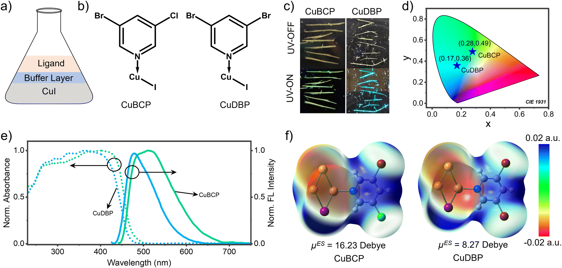 | ||
| Fig. 1 (a) Graphical representation of the three-layer crystallization technique. (b) Molecular structure of CuBCP and CuDBP. (c) Photographs of CuBCP and CuDBP under UV-ON/OFF conditions. (d) CIE coordinates of the CuBCP and CuDBP crystals. (e) Optical absorption and emission spectra of the CuBCP and CuDBP crystals. (f) The electrostatic potential map of monomeric CuBCP and CuDBP compounds with their excited state dipole moment values. | ||
Furthermore, the solid-state optical studies of the crystals revealed a broad absorption band ranging from 250 to 475 nm for CuBCP, and green FL between 450 and 690 nm, peaking at λmax ≈ 525 nm. Its average FL lifetime was found to be τavg = 17 ns. Similarly, CuDBP exhibited an absorption spectrum spanning 250 to 475 nm, with cyan FL ranging from 425 to 650 nm and a peak at λmax ≈ 480 nm (Fig. 1e), which exhibits a blue shift in relation to CuBCP CPs. To find the reason for the blue shift in CuDBP, we performed a time-dependent density functional theory analysis to calculate the molecule's electrostatic potential maps and molecular polarities (Fig. 1f). The excited dipole moment is obtained to be 16.23 Debye and 8.27 Debye, respectively, for CuBCP and CuDBP. The larger excited-state dipole moments in CuBCP CPs result in better stabilisation than CuDBP CPs, which reduces the energy gap between the ground and excited states for CuBCP CPs (Fig. S6, ESI†). This causes a redshift in the FL wavelength for CuBCP.
The HOMO–LUMO energy gap is found to be 1.86 eV for CuBCP and 1.92 eV for CuDBP, which further supports the red-shifted emission band observed for CuBCP compared to CuDBP. The average FL lifetime of CuDBP was measured as τavg = 26 ns (Fig. S7, ESI†). Furthermore, solid-state absolute photoluminescence quantum yield (PLQY) measurements indicated values of ≈4% for CuBCP and ≈21% for CuDBP.
The 1D CPs consist of a multi-fold extended Cu⋯Cu diagonal interaction41 bridge involving alternating copper and iodine atoms, with Cu⋯Cu of 2.840 Å and 2.732 Å, respectively (Fig. 2a and h). The crystallographic b-axis reveals that the bridging iodide ions bind to neighbouring metal centres, forming polymeric Cu2(μ-I)2 chains in both CP crystals. The CuBCP contains the halogen–halogen interactions between C–Cl⋯I (3.711 Å) aligned with the ∠C–Cl⋯I of around 174°. The second halogen interaction in CuBCP was observed between C–Br⋯I (3.716 Å) at ∠C–Br⋯I 168° (Fig. 2b). Similarly, in CuDBP, the halogen interactions were observed between C–Br⋯I with one bromine with the adjacent chain's iodine as 3.729 Å and 3.738 Å corresponding to the angles C–Br⋯I 176° and 168°, respectively (Fig. 2i).42 Such halogen-based intermolecular interactions play a crucial role in governing the mechanical flexibility of these crystals, commonly attributed to the heavy atom effect.43,44 The crystallographic a-axis shows the parallel and alternative top/bottom ligand arrangement in the Cu–I polymeric chain in the elongated direction with 4.213 Å and 4.172 Å for CuBCP and CuDBP, respectively (Fig. 2c and j). This ordered arrangement contributes to the observed mechanical flexibility of the CP crystals.
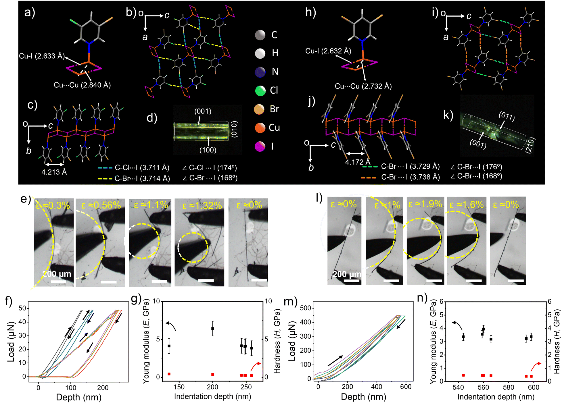 | ||
| Fig. 2 (a) and (h) Single crystal-XRD structures of monomeric units of CuBCP and CuDBP CPs, respectively, displaying various interactions and bond distances. (b) and (c) Molecular packing along the b and a-crystallographic axes, respectively. (d) and (k) Photographs of CuBCP and CuDBP crystals used for SC-XRD analysis, along with their corresponding face indexing, respectively. (i) and (j) Molecular packing of CuDBP along the b and a-axis, respectively, showing two distinguished halogen–halogen interactions. (e) and (l) Photographs of CuBCP and CuDBP microcrystals during a three-point bending test exhibiting their elastic behavior, respectively. (f) and (m) Load (P) vs. depth (h) curves obtained during nanoindentation performed on the widest (100) face of the CuBCP and the widest (011) face of the CuDBP crystals. (g) and (n) Corresponding Young's modulus (E) and hardness (H) values for the same CuBCP and CuDBP crystals. | ||
The mechanical flexibility of the CP crystals was studied by a three-point bending test along the (001/00![[1 with combining macron]](https://www.rsc.org/images/entities/char_0031_0304.gif) ) plane. A sharp needle was used to apply force to the crystal while it was held in place with forceps at both ends, inducing strain through bending. Upon release of the force, the crystal immediately returned to its original shape, confirming its elasticity. The bending-induced maximum strain of CuBCP and CuDBP crystals was calculated to be 1.32% and 1.9%, respectively (Fig. 2e and l). The repeated bending of Cu CPs under multiple cycles of applied external force provides strong evidence of the crystals' elastic behaviour (Videos S1 and S2, ESI†).
) plane. A sharp needle was used to apply force to the crystal while it was held in place with forceps at both ends, inducing strain through bending. Upon release of the force, the crystal immediately returned to its original shape, confirming its elasticity. The bending-induced maximum strain of CuBCP and CuDBP crystals was calculated to be 1.32% and 1.9%, respectively (Fig. 2e and l). The repeated bending of Cu CPs under multiple cycles of applied external force provides strong evidence of the crystals' elastic behaviour (Videos S1 and S2, ESI†).
The qualitative mechanical properties of both CPs were investigated using AFM-based nanoindentation on broader crystal planes. Load (μN) versus displacement (nm) curves were obtained for the (100) plane of CuBCP and the (011) plane of CuDBP using a cone-shaped diamond tip (Fig. S5, ESI†). The significant residual depth observed during tip unloading indicates the crystals’ notable elastic response under mechanical stress (Fig. 2f and m). The mechanical properties calculated using the Oliver–Pharr method revealed that CuBCP exhibited a Young's modulus (E) of 4.45 ± 0.97 GPa and hardness (H) of 0.32 ± 0.08 GPa, whereas CuDBP demonstrated an E of 3.44 ± 0.27 GPa and an H of 0.44 ± 0.03 GPa (Fig. 2g and n, and eqn S4–S6, ESI†). These elastic crystals also show their pseudoplastic behaviour. The high-resolution transmission electron microscopy (HR-TEM) analysis of the CuDBP nanocrystals showed fringes with a d-spacing of 3.6 Å along the (200) plane (Fig. 3d). The bright hexagonal diffraction spots evident in the SAED pattern are indicative of long-range ordered monoclinic systems viewed along the direction close to the hexagonal axis (Fig. 3d and e). To perform an optical waveguiding experiment on the cyan-emissive CuDBP crystal (OW-1), a solution containing microcrystals was drop-cast onto a glass coverslip. A naturally bent, pseudo-plastically attached highly strained (ε ≈ 6%) needle-like nanocrystal (designated as OW-1) with a length of 68 μm and a width of 456 nm was selected for the experiment. The crystal's excitation position-dependent optical waveguiding measurements (Fig. 3a and b) exhibited that the optical loss (α′) increased with increasing signal propagation distance. The low optical loss of 0.026 dB μm−1 highlights the superior waveguiding quality of the crystal in the visible spectral region (Fig. S8, ESI†). Similarly, the optical waveguiding analysis was performed on naturally grown, doubly bent CuBCP crystals (OW-2) holding strain values of ≈0.74% and ≈0.60% (Fig. 3g and h). The optical waveguiding OW-2 crystal exhibited an optical loss of 0.011 dB μm−1 (Fig. 3i, l and Fig. S9, ESI†). The HR-TEM studies provided strong proof of the crystallinity of CuDBP elongated micro-particles. These crystalline monomers are arranged in a highly ordered packing with a d-spacing of 3.4 Å, which correlates with the (101) plane of the SC-XRD data. The selected area of electron diffraction (SAED) analysis revealed distinguishable bright spots, confirming the crystallinity of the CuBCP micro-particles.
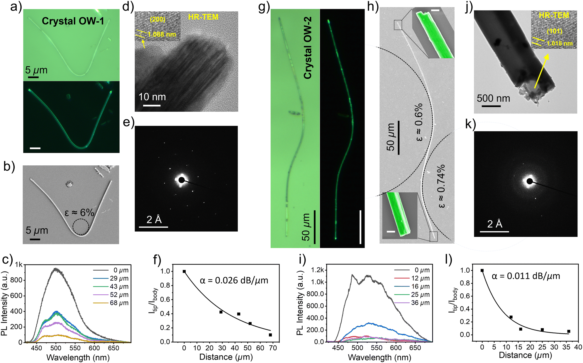 | ||
| Fig. 3 (a) Bright-field (top) and FL (bottom) images of naturally bent CuDBP crystal OW-1. (b) FESEM image of OW-1. (c) Position-dependent FL spectra collected at the crystal tip with various excitation points on OW-1. (d) TEM image showing molecular fringes on the crystalline CuDBP nanowire showing the d-spacing of 3.6 Å. (e) SAED pattern of a CuDBP crystal. (f) and (l) The plot of I tip/I body vs. distance used to calculate the optical loss of OW-1 and -2 crystals. (g) Confocal optical microscopy images showing a naturally bent CuBCP crystal, OW-2. (h) FESEM image of OW-2 (inset shows magnified colour-coded FESEM images of both crystal's tips. Scale: 1 μm). (i) Position-dependent optical spectra collected with varying excitation positions. (j) TEM image showing fringes on crystalline CuBCP nanowires having a d-spacing of 3.4 Å. (k) SAED pattern of a crystalline CuBCP nanowire. | ||
The optical waveguiding in CuBCP was explored to establish the relation between mechanical strain and optical loss. For that, a high aspect ratio, straight microcrystal (OW-3) with a length of about 189 μm and a width of about 560 nm was selected (Fig. 4a and b). First, the unstrained OW-3 was taken, and excitation position-dependent optical waveguiding was performed. The corresponding optical spectra were utilised to estimate the optical loss of α′ ≈ 0.04625 dB μm−1 (Fig. 4 and Fig. S10p, ESI†). Subsequently, the crystal was bent to an arc geometry using the AFM tip with a radius of R2 = 120 μm, and the strain was calculated to be ε ≈ 0.23%. The estimated optical loss for this strain is α′ ≈ 0.05757 dB μm−1 (Fig. 4 and Fig. S10q, ESI†). The crystal was further step by step bent into the arc geometry with a decreasing radius of 67 μm, 40 μm, and 28 μm, and the strain value was estimated to be approximately 0.42%, 0.70%, and 1.06%, respectively. Furthermore, the α′ corresponding to the crystal with the above strain values was calculated to be ≈0.0649, 0.0908, and 0.148 dB μm−1, respectively. This result unveiled that the α increases with the increment of the mechanical strain (Fig. 4a–c and Fig. S10, ESI†).
 | ||
| Fig. 4 (a) Confocal optical microscopy images of a methodically bent CuBCP microcrystal optical waveguide (OW-3), using the micromanipulation technique. (b) Color-coded FESEM image of a bent CuBCP microcrystal. (c) Plot of optical loss vs. strain calculation by the OW-3 during mechanical bending. | ||
The FE-SEM image of a bent crystal with a strain of 1.06% showed the smooth and uniform surface morphology of the OW-3 crystal and the distance between the tips of about 60 μm (Fig. 4b). The straight CuBCP single crystal (width ≈ 1.12 μm; α′ = 0.014 dB μm−1) was selected on substrate-1, and using an AFM tip, it was lifted and transferred to substrate-2, which contains CuDBP single crystal (Fig. S11 and S12, ESI†). It was cut into a desired length (≈110 μm) to get an optical waveguide OW-4 (Fig. S13, ESI†). To fabricate a Y-splitter, OW4 was bent into an arc shape using an AFM tip to a strain value of 1.38% (Fig. S14, ESI†). As the substrate-2 already contains multiple CuDBP single crystals, one of them with a width of ≈1.21 μm and a length of ≈77 μm was selected (labelled as OW-5). The OW-5 crystal was precisely bent, and one of its terminal segments was carefully integrated with the convex region of bent OW-4 to form a Y-geometry (Fig. 5a and Fig. S15, ESI†). The terminal segment of OW-5 was positioned in such a way that both the waveguides could interact via evanescent coupling. The convex area of OW-4 can provide efficient coupling of light to OW-5 and vice versa. The colour-coded FE-SEM images of the Y-splitter show the smooth surface morphology of both crystals and also reveal the large coupling region (J) of ≈4.5 μm for effective energy transfer (ET) in the contact area (Fig. 5b). The optical signal directionality and light-routing capabilities of the fabricated Y-splitter were analyzed by giving an input excitation signal (405 nm) at terminals T1, T2 and T3, and recording the output PL response at the other two terminals (Fig. 5a and b). All the optical properties (emission maximum, PLQY, and excited-state dipole moment) and mechanical characteristics (elastic modulus and hardness) of CuBCP and CuDBP exhibit optimal compatibility for meeting the circuit requirements (Fig. 5i). When the input was given at T1 of the OW-4, it produced an active (A) green FL signal λ1(A) covering the bandwidth of ≈440–710 nm and the reabsorbed passive signal, −λ1(A) covering the bandwidth of ≈450–710 nm transduced to output, T2 (Fig. 5c).
 | ||
| Fig. 5 (a) Optical and FL images of Y-splitter optical components fabricated using CuDBP (OW-4) and CuBCP (OW-5) flexible crystal optical waveguides. (b) Colour-coded FESEM image of the Y-shape optical splitter (inset shows magnified images of the coupling region and tips, scale bar: 200 nm). (c)–(e) FL image of the Y-splitter with excitation at the T1, T2 and T3 ports, respectively. (d)–(h) Optical waveguiding signal spectra at various outputs for input at the T1, T2 and T3 ports, respectively, in the Y-splitter. (i) The optical performance of the Y-splitter tabulated according to the signal observed at various ports against the given input. (j) and (k) Different optical signal types and bandwidths operational in the Y-splitter. | ||
However, as there is no ET, the same signal without any chromatic modulation, passively couples evanescently into OW-5 and propagates towards T3 and is outcoupled as signal −λ1(P) (Fig. 5f). When the input excitation signal was given at T2, the tip generated signal λ1(A) and propagated towards T1 and was outcoupled as −λ1(A), as explained before. However, due to the constrained geometry of the waveguides, this time, the signal could not be entered into OW-5. Hence, no optical signal (0) was detected at T3 during the experiment (Fig. 5d and g). Interestingly, when the input was given at T3 of OW-5, it generated the cyan signal λ2(A) covering the ≈435–690 nm region, which propagated toward the junction couple to OW4, and due to ET, the chromatically modulated light signal λ1(A) was produced outcoupled as reabsorbed green signal, −λ1(A) at T1. No optical signal was observed at T2 due to signal flow restricting the circuit geometry (Fig. 5e and k). Hence, the constructed Y-splitter using CuDBP and CuBCP CPs demonstrates its photonic function as a light signal splitter and chromatic modulator.
The Y-splitter is a unique optical component that guides and splits light into two directions. Such an optical component is well-known in silicon photonics. Here, we are mimicking the optical component for the first time with CP microcrystals, considering the advantages of CPs for splitting and chromatic modulation over silicon-based optical splitters. Thus, the application of the Y-splitter is limited to splitting the signals, but we are extrapolating the advantage of the geometry and using it in a reverse way to get the active and passive signal outputs from the same device.
Conclusions
In summary, we designed and crystallized cyan and green emissive, halo-substituted Cu-pyridyl coordination polymers (CPs). Macro-level three-point bending, micro-level AFM nanoindentation, and micro-level AFM cantilever tip-based bending experiments revealed the elastic and pseudoplastic characteristics of the CPs, respectively. The long, needle-shaped pseudoplastic microcrystals acted as low-loss optical waveguides. The mechanophotonics technique provided CuDBP and CuBCP CP-based hybrid Y-splitters mimicking and advancing the optical component known in Si photonics. Due to the hybrid nature of the fabricated Y-splitter, it could (i) selectively split the light in one direction without chromatic modulation, (ii) simply guide the light without splitting and chromatic modulation, and (iii) chromatically modulate the signal without splitting it. This unprecedented finding paves the way for innovative designs of flexible, high-performance optical devices using luminescent and flexible CP single crystals useful for next-generation integrated photonic circuit devices.Author contributions
The manuscript was written through the contributions of all authors. All authors have given approval to the final version of the manuscript.Conflicts of interest
There are no conflicts to declare.Data availability
The data supporting this article have been included as part of the ESI.† Crystallographic data for CuDBP and CuBCP have been deposited at the Cambridge Crystallographic Data Centre (CCDC) under the CCDC numbers 2432154 and 2434224, and can be obtained from https://doi.org/10.5517/ccdc.csd.cc2mmvlq and https://doi.org/10.5517/ccdc.csd.cc2mq0cr, respectively.Acknowledgements
R. C. acknowledges ANRF-SERB-New Delhi [SERB-STR/2022/00011 and CRG/2023/003911], DST-RSF [DST/INT/RUS/RSF/P-71/2023(G)] for financial support. A. K. thanks PMRF for financial support. P. R. thanks the IOE Project for the fellowship, and B. K. B. is thankful for the IOE PDRF fellowship. The Centre of Modelling, Simulation and Design (CMSD) at the University of Hyderabad is acknowledged for its computational facilities.References
- R. Chandrasekar, Mechanophotonics for Organic Photonic Integrated Circuits, IOP Publishing, London, 2024 Search PubMed.
- R. Chandrasekar, Chem. Commun., 2022, 58, 3415–3428 RSC.
- R. Chandrasekar, Small, 2021, 17, 2100277 CrossRef CAS PubMed.
- C. M. Reddy, R. C. Gundakaram, S. Basavoju, M. T. Kirchner, K. A. Padmanabhan and G. R. Desiraju, Chem. Commun., 2005, 3945–3947 RSC.
- N. Chandrasekhar and R. Chandrasekar, Angew. Chem., Int. Ed., 2012, 51, 3556–3561 CrossRef CAS PubMed.
- S. Ghosh and C. M. Reddy, Angew. Chem., Int. Ed., 2012, 51, 10319–10323 CrossRef CAS PubMed.
- M. Annadhasan, D. P. Karothu, R. Chinnasamy, L. Catalano, E. Ahmed, S. Ghosh, P. Naumov and R. Chandrasekar, Angew. Chem., Int. Ed., 2020, 59, 13821–13830 CrossRef CAS PubMed.
- M. Annadhasan, A. R. Agrawal, S. Bhunia, V. V. Pradeep, S. S. Zade, C. M. Reddy and R. Chandrasekar, Angew. Chem., Int. Ed., 2020, 59, 13852–13858 CrossRef CAS PubMed.
- S. Hayashi and T. Koizumi, Angew. Chem., Int. Ed., 2016, 55, 2701–2704 CrossRef CAS PubMed.
- H. Liu, Z. Lu, Z. Zhang, Y. Wang and H. Zhang, Angew. Chem., Int. Ed., 2018, 57, 8448–8452 CrossRef CAS PubMed.
- Y. S. Zhao, Organic Nanophotonics: Fundamentals and Applications, 2014, p. 208 Search PubMed.
- M. Godumala, A. V. Kumar and R. Chandrasekar, J. Mater. Chem. C, 2021, 9, 14115–14132 RSC.
- A. Vinod Kumar, P. Pattanayak, A. Khapre, A. Nandi, P. Purkayastha and R. Chandrasekar, Angew. Chem., Int. Ed., 2024, 63, e202411054 CrossRef CAS PubMed.
- K. Takazawa, Y. Kitahama, Y. Kimura and G. Kido, Nano Lett., 2005, 5, 1293–1296 CrossRef CAS PubMed.
- X. Wang, Q. Liao, H. Li, S. Bai, Y. Wu, X. Lu, H. Hu, Q. Shi and H. Fu, J. Am. Chem. Soc., 2015, 137, 9289–9295 CrossRef CAS PubMed.
- W. Zhang, J. Yao and Y. S. Zhao, Acc. Chem. Res., 2016, 49, 1691–1700 CrossRef CAS PubMed.
- Y. S. Zhao, A. Peng, H. Fu, Y. Ma and J. Yao, Adv. Mater., 2008, 20, 1661–1665 CrossRef CAS.
- N. Chandrasekhar, M. A. Mohiddon and R. Chandrasekar, Adv. Opt. Mater., 2013, 1, 305–311 CrossRef.
- A. Khapre, A. V. Kumar and R. Chandrasekar, Laser Photonics Rev., 2025, 19, 2400278 CrossRef CAS.
- J. Ravi and R. Chandrasekar, Adv. Opt. Mater., 2021, 9, 2100550 CrossRef CAS.
- J. Ravi, M. Annadhasan, A. Vinod Kumar and R. Chandrasekar, Adv. Funct. Mater., 2021, 31, 2100642 CrossRef CAS.
- A. V. Kumar and R. Chandrasekar, Adv. Opt. Mater., 2023, 11, 2201009 CrossRef CAS.
- A. V. Kumar, M. Rohullah, M. Chosenyah, G. Sindhuja and R. Chandrasekar, Angew. Chem., Int. Ed., 2025, e202502122 CAS.
- M. Chosenyah, A. Vinod Kumar and R. Chandrasekar, IEEE Photonics Technol. Lett., 2024, 36, 1093–1096 CAS.
- A. V. Kumar, M. Godumala, J. Ravi and R. Chandrasekar, Adv. Opt. Mater., 2024, 12, 2302807 CrossRef CAS.
- A. V. Kumar, M. Godumala, J. Ravi and R. Chandrasekar, Angew. Chem., Int. Ed., 2022, 61, e202212382 CrossRef CAS PubMed.
- D. Wang, W. Hu, B. J. Reinhart, X. Zhang and J. Huang, ACS Appl. Mater. Interfaces, 2022, 14, 42171–42177 CrossRef CAS PubMed.
- A. Ritchhart, A. S. Filatov, I. R. Jeon and J. S. Anderson, Inorg. Chem., 2023, 62, 2817–2825 CrossRef CAS PubMed.
- C. Rajadurai, O. Fuhr, R. Kruk, M. Ghafari, H. Hahn and M. Ruben, Chem. Commun., 2007, 2636–2638 RSC.
- M. Liu, H. S. Quah, S. Wen, J. Wang, P. S. Kumar, G. Eda, J. J. Vittal and W. Ji, J. Mater. Chem. C, 2017, 5, 2936–2941 RSC.
- S. K. Dubey, B. Biswas, D. Halder, S. Mallick, I. Saha, K. Gupta, S. Giri, A. S. Patra, C. Rizzoli, A. K. Meikap, S. Bhattacharjee and R. Saha, Cryst. Growth Des., 2023, 23, 7066–7075 CrossRef CAS.
- S. Chen, M.-P. Zhuo, X.-D. Wang, G.-Q. Wei and L.-S. Liao, PhotoniX, 2021, 2(1), 2 CrossRef.
- X. Gu, Y. Wei, N. Yu, J. Qiao, Z. Han, Q. Lin, X. Han, J. Gao, C. Li, J. Zhang, X. Hao, Z. Wei, Z. Tang, Y. Cai, X. Zhang and H. Huang, CCS Chem., 2023, 5, 2576–2588 CrossRef CAS.
- M. Đaković, M. Borovina, M. Pisačić, C. B. Aakeröy, Ž. Soldin, B. Kukovec and I. Kodrin, Angew. Chem., Int. Ed., 2018, 130, 15017–15021 CrossRef.
- B. Bhattacharya, A. A. L. Michalchuk, D. Silbernagl, M. Rautenberg, T. Schmid, T. Feiler, K. Reimann, A. Ghalgaoui, H. Sturm, B. Paulus and F. Emmerling, Angew. Chem., Int. Ed., 2020, 59, 5557–5561 CrossRef CAS PubMed.
- B. B. Rath and J. J. Vittal, Chem. Mater., 2021, 33, 4621–4627 CrossRef CAS.
- S. Panbarasu, A. Khapre, M. Chosenyah, A. V. Kumar and R. Chandrasekar, Chem. Mater., 2023, 35, 10169–10177 CrossRef CAS.
- C. Sun, J. Zhao, Z. Wang, L. Du and W. Huang, Optik, 2019, 180, 866–872 CrossRef CAS.
- C. Ozcan, J. S. Aitchison and M. Mojahedi, Photonics, 2023, 10, 1310 CrossRef CAS.
- C. Von Essen, K. Rissanen and R. Puttreddy, Materials, 2019, 12, 3305 CrossRef CAS PubMed.
- N. V. S. Harisomayajula, S. Makovetskyi and Y.-C. Tsai, Chem. – Eur. J., 2019, 25, 8936–8954 CrossRef CAS PubMed.
- Deposition numbers 2434224 (for CuBCP) and 2432154 (for CuDBP) contain the supplementary crystallographic data for this paper. These data are provided free of charge by the joint Cambridge Crystallographic Data Centre and Fachinformationszentrum Karlsruhe Access Structures service.
- T. Pramanik, S. Sarkar and T. N. G. Row, Cryst. Growth Des., 2021, 22, 48–53 CrossRef.
- B. Bhattacharya, A. a L. Michalchuk, D. Silbernagl, N. Yasuda, T. Feiler, H. Sturm and F. Emmerling, Chem. Sci., 2023, 14, 3441–3450 RSC.
Footnote |
| † Electronic supplementary information (ESI) available. CCDC 2432154 (CuDBP) and 2434224 (CuBCP). For ESI and crystallographic data in CIF or other electronic format see DOI: https://doi.org/10.1039/d5tc02090e |
| This journal is © The Royal Society of Chemistry 2025 |