
 Open Access Article
 This Open Access Article is licensed under a
 Creative Commons Attribution 3.0 Unported Licence
Emerging avalanche field-effect transistors based on two-dimensional semiconductor materials and their sensory applications
Ehsan Elahi†
 *a,
Muhammad Farooq Khan†
b,
Jamal Azizc,
Umer Ahsan
a,
Payal Chauhan
a,
Mohammed A. Assirid,
Kalyan Jyoti Sarkar
a,
Umer Asgheref and
Zdenek Sofer
*a
*a,
Muhammad Farooq Khan†
b,
Jamal Azizc,
Umer Ahsan
a,
Payal Chauhan
a,
Mohammed A. Assirid,
Kalyan Jyoti Sarkar
a,
Umer Asgheref and
Zdenek Sofer
*a
aDepartment of Inorganic Chemistry, University of Chemistry and Technology, Prague, Technická 5, Prague 616628, Czech Republic. E-mail: elahie@vscht.cz; Zdenek.Sofer@vscht.cz
bDepartment of AI Convergence Electronic Engineering, Sejong University, Seoul, Republic of Korea
cChair of Smart Sensor Systems, University of Wuppertal, Wuppertal, Germany
dDepartment of Chemistry, College of Science, King Khalid University, P.O. Box 9004, Abha, 61413, Saudi Arabia
eLaboratory of Human Factors and Automation in Aviation, Department of Air Transport, Faculty of Transportation Sciences, Czech Technical University in Prague (CTU), 128 00 Prague, Czechia
fSchool of Interdisciplinary Engineering and Sciences (SINES), National University of Sciences and Technology (NUST), Islamabad, 44000, Pakistan
First published on 11th July 2025
Abstract
Recently, two-dimensional (2D) layered semiconductors have been the subject of promising research work due to their intriguing physical and chemical characteristics. In electronic nano-devices, impact ionization is a viable condition to investigate or probe the level of sensitivity upon the application of external stimuli. However, avalanche field-effect transistors (FETs) have emerged as promising candidates for a wide range of sophisticated applications, especially for sensing traits. In this review, we explore the incorporation of 2D materials into avalanche FETs, highlighting their auspicious properties such as high carrier mobility, variable band gaps, and atomic thickness, which provide significant advantages over typical materials. 2D materials significantly improve the sensitivity, speed, and power efficiency of avalanche FETs. This study also encompasses the advances in photo-, bio- and gas-sensing technologies, emphasizing their implications in contemporary applications such as optoelectronics, imaging, and environmental monitoring. Thus, our review provides a thorough investigation of material attributes, device architecture, and prospective applications by establishing avalanche FETs with 2D materials as the keystone in power and rectifying applications.
 Ehsan Elahi | Dr Ehsan Elahi currently works as a postdoctoral researcher in the Sofer group at the Department of Chemistry, University of Chemistry and Technology (UCT), Prague, Czech Republic. He obtained his MSc in Electronics from Quaid-i-Azam University Islamabad, Pakistan and MPhil from Riphah International University Lahore Campus, Punjab, Pakistan. He attained a doctorate degree (PhD) from the Department of Physics, Sejong University, Seoul, South Korea in 2024. Ehsan's research interests include 2D materials (TMDCs), 2D ferromagnetic materials, electronics, optoelectronics, spintronics, and spin-caloritronics. |
 Muhammad Farooq Khan | Dr Muhammad Farooq Khan is an assistant professor at the Department of AI Convergence Electronic Engineering, Sejong University, Republic of Korea. He earned his PhD (Physics) from Sejong University in 2018. After that, he was a postdoc fellow at Yonsei University in 2019. His research primarily focused on nanofabrication of electronic, memory, and energy harvesting devices manifested by two-dimensional layered semiconductor materials. His contributions extend beyond academia; he successfully won two research grants from the National Research Foundation (NRF) of South Korea and has authored a book chapter on “2D Material Photonics and Optoelectronics.” In addition, he is serving as a referee for various scientific journals ensuring the dissemination of high-quality research. |
 Umer Ahsan | Mr Umer Ahsan holds a Master of Science in Physics from COMSATS University Islamabad, Lahore Campus, completed in 2020. He is pursuing a PhD in Chemical Technology at the University of Chemistry and Technology, Prague, where his doctoral research focuses on synthesis, characterization, and device integration of advanced two-dimensional transition metal dichalcogenides and their novel alloys. His work explores applications in next-generation nanoelectronic and optoelectronic devices—including field-effect transistors, photodetectors, and chemical sensors—by investigating structure–property relationships to enhance performance. He has authored several peer-reviewed articles advancing sustainable, high-performance electronic systems. |
 Payal Chauhan | Dr Payal Chauhan is a Marie Skłodowska-Curie Actions postdoctoral ERA Fellow in the Sofer Group at the University of Chemistry and Technology (UCT), Prague, Czech Republic. She received her PhD in Physics from the Department of Physics, Sardar Patel University, Gujarat, India, in 2022. Prior to joining UCT, she held a postdoctoral position at CHARUSAT University, Gujarat, India. Her current research focuses on two-dimensional composite materials for electrocatalytic applications, including water splitting, supercapacitors, and anion exchange membrane electrolyzers for seawater electrolysis, aiming to advance sustainable energy and hydrogen production technologies. |
 Kalyan Jyoti Sarkar | Dr Kalyan Jyoti Sarkar received his PhD degree from the Indian Institute of Technology Kharagpur (IIT Kharagpur), India in 2020. Currently he is working as a postdoctoral researcher at Sofer Group, University of Chemistry and Technology Prague (UCT Prague). Prior to joining the Sofer Group in January 2022, he was a SERB National Postdoctoral Fellow at the Indian Institute of Science Bangalore (IISc Bangalore). He has also worked as a research associate-I in the QuEST-DST project for six months at the Indian Institute of Science Education and Research, Thiruvananthapuram (IISER TVM). His research focus is on fabrication and characterization of 2D material-based devices for optoelectronics, memory applications, and quantum transport studies. |
 Zdenek Sofer | Dr Zdeněk Sofer has been a full professor at the University of Chemistry and Technology Prague, Czech Republic, since 2019. He also received his PhD from the University of Chemistry and Technology Prague in 2008. During his PhD, he spent one year at Forschungszentrum Julich (Peter Grünberg Institute, Germany), followed by postdoctoral experience at the University of Duisburg-Essen, Germany. His research interests include semiconductors and 2D materials, their synthesis, crystal growth, chemical modifications and functionalization. He is particularly focused on various applications of two-dimensional materials including energy storage and conversion. |
1. Introduction
After the discovery of graphene,1 the scientific community has explored two-dimensional (2D) layered semiconductor materials that have been recognized as promising contenders for a variety of applications due to their exceptional characteristics, which include a dangling-bond-free surface, rich physical properties, and flexibility at the atomic level.2–6 Due to high contact resistance, large leakage current, and short channel effects, the conventional solid-state technology invokes to meet the need for miniaturization in electronic devices.7,8 The potential for the revolutionary role of 2D materials in nanoelectronics and optoelectronics is essentially admired in the modern era.9–11 This motivates the investigation of 2D semiconductors, such as TMDCs,3,12–17 group III chalcogenides (e.g., InSe, GaSe, In2Se3, etc.),18–21 and mono-elemental materials (e.g., phosphorene, tellurene, etc.).22–24 Therefore, 2D semiconductors are extremely useful for developing electronic,25,26 photonic, memory,27 sensing28 and neuromorphic devices29–32 due to their exclusive electronic band structures and atomically thin physical architecture.12,33,34 These materials can play a substantial role in accelerating the advancement of both electronics35–37 and optoelectronics38–40 due to their ease of fabrication and integration (without the need for strict lattice matching or epitaxy), high carrier mobility,18,19 strong light–matter interactions,41,42 and strong electrostatic control.43 2D semiconductor technology is now advanced enough to be compatible with Si-based electronics, allowing diversity in fabrication of nano-devices and circuit-level configurations on the wafer scale.44–471.1. Avalanche breakdown phenomenon
In recent years, a few efforts have been made towards impact ionization in avalanche transistors made using 2D materials. Avalanche FETs48 have been gaining gigantic attention in electronics due to their ability to perform photo-, gas- and bio-sensing (Fig. 1a). The avalanche breakdown is a phenomenon in semiconductor devices where a sudden increase in current occurs due to the ionization of carriers (holes and electrons) within the material. This happens when an electric field (E-field) across the p–n junction is sufficiently strong, leading to rapid multiplication of charge carriers. The process of avalanche multiplication occurs when an extremely fast charge collides with atoms in a substance, creating electron–hole pairs that are assisted by free valence electrons. The threshold of E-field at which avalanche breakdown originates and a material transits from a higher-resistance state to a lower-resistance state is used to interpret the electrical breakdown voltage (VEB); the avalanche breakdown region is shown in Fig. 1(b). It is a crucial factor to figure out the highest voltage that an electronic device can tolerate before suffering permanent damage of the crystalline structure of materials. The relationship between VEB and the dimensions of the channel material, such as channel length and thickness, profoundly influences the device configuration, functionalities and fabrication. The electrical breakdown observed in 2D-FETs under a high E-field originated from impact ionization within the 2D channel, commonly referred to as avalanche multiplication.49 The critical electric field (ECR) and impact ionization rate (α) are the key parameters for quantifying the avalanche breakdown mechanism. The ECR is referred to as the lowest E-field required for the avalanche multiplication and α (cm−1) is referred to as the number of electron–hole pairs produced per unit distance travelled by the hot carrier. Here, ECR = VEB/L, where VEB is the value of source–drain voltage (VDS) at which the breakdown begins. When the device operates under the breakdown zone, the carrier multiplication gain (G) becomes limited, making it suitable for photon energy discernment, and the device output current is proportional to the incoming photon power. Conversely, when the device functions above the breakdown voltage, known as Geiger mode, an incident photon can initiate avalanche breakdown, resulting in substantial carrier multiplication. This multiplication can be unlimited and may instigate a self-sufficient avalanche development, thereby assisting single-photon detection.50 The breakdown behavior of some 2D materials, such as MoS2,51 WSe2 and graphene,52 has been the subject of recent investigations. Along with various other device applications, the 2D materials including graphene, TMDCs and black phosphorus (BP) have provided new opportunities for improving the performance of avalanche FETs.51,53,54 | ||
| Fig. 1 (a) Schematic of an avalanche FET/avalanche photosensor: which can be further used for gas and biomolecule sensing. (b) Schematic representing the avalanche breakdown region in the form of the (I–V) curve. The band configuration of the p–n heterojunction: (c) under low bias (V < VEB). (d) High bias V > VEB. | ||
An avalanche photodiode (APD) is an enormously sensitive photodetector that can transform light into current/voltage. Basically, the APD operates at high reverse bias voltages of tens or even hundreds of volts.55 In this phase, the E-field accelerates the photogenerated electron–hole pairs, allowing them to impact ionize and produce additional carriers. The APD can therefore be employed as an incredibly very sensitive detector that requires minimal electrical intensification. Furthermore, due to the atomically thin nature, 2D materials may be able to start the impact ionization in a short active region (<10 nm) with relatively low electrical bias, resulting in carrier multiplication with a high G and better noise performance owing to its nanoscale active zone. Fig. 1(c and d) depicts the heterojunction band alignments at various bias voltages to evaluate the intrinsic phenomenon of the avalanche photodiode.56 The pink area shows the depletion zone in the p-type/n-type heterojunction. When the FET is under bias, the applied voltage aligns with the built-in E-field. At low voltages, as demonstrated in Fig. 1(c), the external E-field is insufficient to cause avalanche breakdown, limiting the performance of the device to a typical photodetector with limited gain. Fig. 1(d) depicts the device's band alignment at high bias voltage, resulting in carrier multiplication via the avalanche process.56 Increasing bias voltage at the p–n junction accelerates photogenerated carriers in the E-field, resulting in more energy. Carrier multiplication generates more electron–hole pairs, significantly increasing photocurrent.57,58 The key metrics parameters of several types of APDs based on 2D materials and their heterostructures are compiled in Table 1.55,59 EQE is defined as the ratio of the number of collected electrons to the number of injecting photons, which is equivalent to  .60,61 Here, Iph is the change in photocurrent, λ is the wavelength of the incident light, h is Planck's constant, c is the speed of light and P is the incident optical power. Nevertheless, 2D photodetector devices use impact-ionized carrier multiplication, and all incident photons are not absorbed to generate free electron–hole pairs to contribute to a photocurrent; their EQE is less than one. However, due to the high Schottky barrier among the 2D channel and metal contacts, the majority of 2D APDs require a significantly high bias in order to commence impact ionization. In 2D APDs, the VEB can be decreased by substituting 2D vdW heterojunctions for metal/semiconductor Schottky junctions. Thus, further developments in 2D-APDs that operate at room temperature with low bias and high gain (G) are required. Responsivity (R),62,63 detectivity (D*)64,65 and EQE66,67 are the important parameters for the photodetection phenomenon.67 R is defined as the ratio of the photocurrent to the incoming light power:
  ,68,69 here A is the effective area and P is the incident power density. D* is a term that typically refers to the ability of a sensor to detect a signal or stimulus
  .70 On the other hand, for outstanding performance of the sensor, and human–computer communication applications, piezotronic and piezo-phototronic devices have been constructed.2,71,72 Examples of these devices include piezoelectric FETs,73 nanogenerators,73 solar cells,74 phototronic photocells73 and piezotronic strain sensors.75 Monolayer MoS2 was used to produce piezotronic transistors.76 The piezotronic GaN tunnelling junction responded quickly to external mechanical stimuli, taking only a response time of 4.38 ms.76 GaN vertical nanowires have a temporal response of less than 5 ms.77 In general, the piezoelectric field and potential govern the built-in field in the p–n junction, as well as the height of the barrier at the metal–semiconductor interface.78,79 The piezotronic devices built with multijunctions have a gauge factor above 104 and may be used as ultra-high sensitivity strain sensors, due to integrating piezoelectric control with bipolar transistor amplification.80 However, there has always been a difference between advanced applications and basic research. The absence of a consistent and practical method for characterizing their characteristics, which ought to be well-suited with the conventional photodetector performance assessment scheme, has been one of the primary causes of this disparity. Determining the level of interoperability between laboratory prototypes and industry technology is crucial. We present broader principles for the evolution of the figures of merit for 2D-based devices and looked at frequent instances in which the particular D*, R, Idark, and speed might be misjudged.
| Materials | Avalanche device type | Responsivity (R) (A W−1) | Detectivity (D*) (Jones) | Rise/fall time (s) | Gain (G) | λ (nm) | EQE | Ref. |
|---|---|---|---|---|---|---|---|---|
| MoS2 | Phototransistor | 3.4 × 10⁷ | 4.3 × 10¹⁶ | 27/1.2 s | — | 520 | ≈8.1 × 10⁹% | 97 |
| Bi2O2Se | Photodiode | 3 × 10³ | 4.6 × 10¹⁴ | 2.5 μs | 400 | 515 | — | 222 |
| BP | Photodetector | 160 | — | — | 7 | 520 | 382 × 102% | 59 |
| WSe2 APD | Phototransistor | 5910 | 5.3 × 10¹² | 8/8.2 μs | 500 | 532 | — | 109 |
| WSe2/WS2 | FET | 135 | 1.3 × 10¹² | 131.8/146.5 μs | — | 400–1100 | — | 116 |
| BP/InSe | Photodiode | 80 | — | — | 104 | 4 μm | 24.8 × 10²% | 165 |
| MoS2 | Photodetector | 104 | 2 × 10¹² | — | 24 | 532 | — | 100 |
| WSe2/MoS2 | Photodiode | 88 μ | — | — | ≈1300 | 532 | — | 117 |
| InSe APD | Photodetector | — | — | 87 μs | 152 | 543 | 866% | 141 |
| ZnO | Photodetector | 1.7 × 10⁴ | 3.2 × 10¹² | 20 ns/98.9 ns | 294 | 367 | — | 138 |
| p-Ge/n-MoS2 | Photodiode | 170 | — | 357/365 μs | 320 | 532 | — | 244 |
| MoTe2/WSe2/MoTe2 | Photodiode | 6.02 | 7.24 × 10⁹ | 475 ms | 587 | 400–700 | 1406% | 245 |
| Gr/epitaxial silicon | Photodetector | 0.38 | 6.63 × 10¹² | 1.4 μs | 1123 | 300–1100 | 60% | 218 |
| InSe APD | Photodetector | 1 × 10⁵ | 7.3 × 10¹² | 1 ms | 500 | 405–785 | — | 223 |
| MoS2-WSe2 | Bionic | 7.6 × 10⁴ | — | 108/268 μs | 1.5 × 10⁴ | 635 | 107% | 241 |
| WS2 | Photodetector | 74 | 1.45 × 10¹³ | — | — | 532 | — | 54 |
| Monolayer MoS2 | Phototransistor | 8.84 × 10⁸ | 1.65 × 10¹³ | 2 ms | — | 450–650 | — | 246 |
| Pt/WSe2/Ni APD | Photodetector | ≈0.28 | — | 45/50 μs | 5 × 10⁵ | 520 | 60% | 158 |
This review article explains the latest advancements in avalanche FETs that use the distinctive characteristics of 2D materials. In addition, we also explore the potential applications of avalanche FETs in sensing technology, which is becoming more important for recent applications of drug screening, healthcare, and cybersecurity systems. To understand the use of 2D semiconductors in electronics, optoelectronics, and sensing technology as avalanche FETs, it is important to explore fundamental concepts and recent breakthroughs. Finally, we discuss the challenges and potential of 2D semiconductor-based devices for practical applications and their scalability, which should be addressed by both academic and industrial researchers. Our perspective can assist academia for a better understanding of 2D semiconducting materials and their fundamental concepts with deep insights.
2. Avalanche breakdown phenomena in 2D and TMDC materials
2.1. Avalanche effect in MoS2-based FETs
TMDC nanosheets have gained popularity due to the lack of dangling bonds on their surface, their exceptional mechanical flexibility, and their high surface-to-volume ratio.81–83 Exploration has focused on layered MoS2 for its exceptional electrical properties and thickness-dependent band configuration, which shifts from an indirect bandgap of 1.2 eV to a direct bandgap of 1.8 eV with fewer layers.84–86 MoS2 has the potential to revolutionize electronics, including ultrathin transparent FETs,87,88 logic circuits,89,90 and sensor applications.91–93 To employ MoS2 in spatial integrated electrical proposals and applications, FET channel lengths needed to be reduced to sub-micrometers. As a result, exposure to strong lateral E-fields may cause electrical breakdown. Furthermore, the electronic band configuration in semiconductors has an impact on the electrical breakdown. As MoS2-FETs show the quantum confinement effect, the thickness of MoS2 determines the electrical breakdown in the device. Under strong E-fields, the electrical characterization of MoS2 is rare due to thermal breakdown as the channel layer's MoS2 offers poor heat dissipation capability.94,95 The significant heat resistance of insulating materials like SiO2 intensifies this phenomenon.96 For these motives, to avoid thermal breakdown due to Joule heating, most of electrical tests in MoS2 FETs have been carried out in the linear domain with smaller VDS. Here, we review the investigation of avalanche multiplication-related electrical breakdown processes in MoS2 FETs with various channel lengths and thicknesses.51 By varying the number of stacking layers, one can control the avalanche multiplication by modifying band configuration in MoS2 due to the phenomenon's quantum confinement impact. Fig. 2(a) displays the optical image of the device based on MoS2 exfoliated flakes with Ti/Au metal contacts. The impact of high E-field on the electrical breakdown was investigated with different channel lengths (1.49, 1.95, 3.42, and 4.97 μm) with uniform thickness of the MoS2 layer (∼2.4 nm). The electrical characteristics of the devices were checked at room temperature. The adsorbed air molecules on MoS2 reduce the out-of-plane phonon vibration as observed, thus reducing energy dissipation by electron–phonon scattering.51 As a result, electrical breakdown in the air can happen at lower VEB. Analyzing the normalized IDS–VDS curves reveals that as the channel length is raised, the early voltage VEB is accompanied by a sudden rise in channel current and switched to the positive VDS as represented in Fig. 2(b). The impact of temperature on avalanche multiplication has also been examined with a MoS2 flake of 17 nm thickness. The measurements were conducted at a fixed VGS of 0 V while varying the temperature from 80 to 300 K. Fig. 2(c) demonstrates that the normalized IDS experienced a rapid increase in the low E-field region until it reached its saturation value. This occurred as the thermal energy supplied to the electron surpasses the Schottky barrier at the junction between the metal electrode and MoS2 layer, as indicated by the low E-field regime. Under conditions of high E-field, the electrons had enough energy to traverse the Schottky barrier and initiate interactions with optical phonons. Consequently, the normalized IDS declined as temperature increased owing to the dissipation of energy resulting from the interaction with optical phonons, as seen with the high E-field. The ECR values at the onset of avalanche multiplication were similarly influenced by temperature since a greater E-field was necessary to counterbalance the energy dissipation caused by electron–phonon scattering with increasing temperature. These findings provide significant evidence for the impact of temperature-dependent electron–phonon scattering on the generation of electron–hole pairs. This behaviour may be explained by two compensatory factors: firstly, a greater temperature enhances electron–phonon scattering, which has a negative influence on impact ionization. Secondly, it decreases the bandgap energy of MoS2, leading to enhanced charge carrier concentration, which has a significant influence on impact ionization. The effects of carrier concentration and E-fields on electrical breakdown imply that the electrical breakdown in MoS2 FETs arises from avalanche multiplication. The occurrence of avalanche multiplication was contingent upon the thickness of MoS2. The impact of electron–phonon scattering and the power law analysis of the correlation between ECR and bandgap energy demonstrated that the avalanche multiplication characteristics in MoS2 agreed with those seen in 3D semiconductors. This research aims to enhance comprehension of the electrical breakdown events in MoS2 when exposed to strong E-fields. Additionally, it will offer valuable understanding for the future accomplishment of controllable avalanche multiplication properties, which are now only achievable in thickness-dependent 2D layered MoS2 and other TMDCs. For instance, the reliance of “ECR” and “α” on the thickness of the MoS2 layer was significantly associated with the quantum confinement effect in a 2D layer as observed in this study. On the other hand, the authors demonstrated an ultrasensitive avalanche device that utilizes chemical vapor deposition (CVD) to produce monolayer MoS2,97 The optical picture of CVD-grown MoS2 flakes is shown in Fig. 2(d). Fig. 2(e) displays an optical image of the fabricated device based on the MoS2 FET. “Au” is utilized for metal electrodes, while a highly p-doped Si with a resistance of about 5 × 10⁻³ Ω cm was employed as the back gate. A certain portion of the MoS2 flakes was chosen to be utilized as a FET channel, and it was placed onto an h-BN flake. The device illustrates the electrical breakdown phenomenon of MoS2 FETs under high VDS at different VGS levels.97 The observed breakdown at various VGS levels is shown in Fig. 2(f). At VGS values of −10, −20, −30, −40, and −50 V, there is a noticeable sharp rise in both IDS and VDS. Typically, drain-induced barrier lowering (DIBL), thermal breakdown, junction punch through, and avalanche carrier multiplication are the four major factors that might result in a rapid increase in IDS of FETs. DIBL represents a potential short-channel effect in MoS2 FETs. Monolayer MoS2's electrostatic properties result in low DIBL even in ultra-short channel devices.51,98 MoS2 FETs fabricated on a SiO2 substrate show little temperature rise. Given that h-BN has a much higher thermal conductivity (∼420 W m−1 K−1) than SiO2 (∼1.40 W m−1 K−1), this device architecture would be less affected by the thermal impact of Joule heating than MoS2 FETs on a SiO2 substrate. Accordingly, thermal breakdown is also not a likely cause for an unexpected spike in IDS. When the depletion zones between the bulk and n+ – drain contact and the p-bulk and n+ – source contact overlap, the junction punch-through effect occurs, enabling IDS to pass through the overlapped depletion regions.99 The previous work51 suggests that other possible causes of the observed breakdown mechanism such as DIBL or thermal effects can be similarly neglected, and the breakdown phenomenon can be attributed to avalanche multiplication. It's interesting to note that the breakdown is closely correlated with the value of VGS at which VEB and ΔIDS/ΔVDS were measured. VEB and ΔIDS/ΔVDS values dropped when VGS went from −50 V to −20 V. However, it was not possible to notice a significant rise in IDS at VGS = −10 V (Fig. 2(f)). This can be attributed to an excessively high channel current (IDS) caused by the gate-field-induced carriers prior to the avalanche breakdown. It is evident that the compliance current was attained at a VDS value of 48.5 V, even lower than VEB (49.5 V) for VGS = −20 V, while the IDS was measured at VGS = −10 V. Overall, the modification of VGS may be used to explain the observed dependency of VEB on VGS by altering the height of contact barrier between the channel and metal electrodes. Since greater E-fields in the channel are felt by electrons inoculated from the source to MoS2, when VDS increases, the value of ΔIDS/ΔVDS increases with an increase in VEB, resulting in a drop in VGS. The fundamental features of breakdown processes in MoS2 FETs might also be examined using the electrical characteristics that were acquired. The formula51 for calculating the multiplication factor (M), or the amount of channel current generated by the electrical breakdown, is| M(VDS) = IDS(VDS)/IDS(VDS = VEB) = IDS(VDS)/Isat | (1) |
 ” is a function of VDS/VEB. Empirically, the following equation signifies the link between “
 ” and VDS/VEB.
 | (2) |
 | ||
| Fig. 2 (a) Optical image of an MoS2-based device with varying channel lengths. (b) Normalized IDS of the MoS2 FET explored at fixed VGS = 0 V and different channel lengths; the breakdown voltages with E-fields are indicated by coloured dashed lines. (c) Normalized IDS associated with E-field recorded at VGS = 0 V at different temperatures between 80 and 300 K. Figures (a)–(c) are reproduced with permission from ref. 51, ACS Nano (2018). (d) Optical image of the CVD-grown MoS2. (e) Optical image of the fabricated device based on the structure h-BN/MoS2. (f) IDS–VDS characteristic curve at different VGS values. Figures (d)–(f) are reproduced from ref. 97, Copyright, Advanced Science (2021). | ||
Here, the fitting equation may be used to obtain “m”.100 As in other studies, the fitting was carried out in this case close to the ln (VDS/VEB) value of 0.05, that is, shortly after the breakdown began.59,100 Overall, it was shown that the interaction between carrier injection via the contact barrier and carrier multiplication by avalanche breakdown is crucial. This work offers a prevailing approach to enhance the performance of avalanche devices and provides a thorough knowledge of thin avalanche FETs, which are uninvestigated areas of investigation in electronics and optoelectronics.
2.2. Absorption-multiplication avalanche WSe2-FETs
It has been established that avalanche devices based on 2D semiconductors have achieved improved performance and efficient G. Here, we reviewed an avalanche device based on the Au/WSe2/Ge structure, where infrared absorption and avalanche zones are observed for the Au/WSe2 Schottky-based junction utilizing the germanium (Ge) substrate, correspondingly. Fig. 3(a) presents the schematic illustration of the Schottky heterojunction (S-HJ) based separate absorption multiplication (SAM) device with its circuitry representing the grounded source terminal Ge node and the applied negative drain bias; the inset displays the equivalent circuit of the device, wherein the resistance of the WSe2 channel material is distributed into R1 and R2, and the Schottky contacts of WSe2/Au are symmetrical to the Schottky diodes S1 (drain node) and S2 (source node) as demonstrated in the inset of Fig. 3(a). Furthermore, the WSe2/Ge junction forms the diode (D1), which is what gives the device its infrared detecting capability. The device's fundamental electrical properties are displayed in Fig. 3(b), where the curves representing the drain current and Ge-node current vs. drain voltage are represented by the black solid line and the red dashed line, respectively. The drain current and Ge-side current are 2 × 10⁻¹¹ A and 3 × 10⁻¹² A, correspondingly, when the bias voltage is −1 V. Both the D1 and S1 Schottky diodes are reverse biased when the VDS is negative, and the reverse leakage current gradually rises as the VDS rises. The significant rise in drain current seen at −25.5 V is ascribed to the device's critical breakdown. It is noteworthy that only the drain current had a sudden rise upon reaching the breakdown, whilst the bulk Ge side current did not exhibit a sharp increase. This suggests that D1 diodes are not susceptible to breakdown under high reverse voltages. As an outcome, the breakdown in the S-HJ-SAM device happens in the WSe2 channel around the Au/WSe2 Schottky diode (interface S1). The device temperature-dependent I–V characteristics are shown in Fig. 3(c). When the temperature drops, the breakdown voltage (VEB) decreases as well. This characteristic demonstrates that the avalanche effect dominates the breakdown at high bias voltages. At higher temperatures, carriers lose more energy owing to the lattice scattering events, leading to a positive temperature coefficient for avalanche breakdown voltage compared to lower temperatures. At greater temperatures, carriers require a higher bias voltage to achieve adequate energy for impact ionization.101 High G for an APD based on the WSe2/Ge heterojunction remains problematic due to tunnelling effects. However, the S-HJ SAM device offers a novel approach of designing avalanche breakdown devices. | ||
| Fig. 3 (a) Schematic illustration of the S-HJ SAM device with the electrical structure: inset displays the equivalent circuit. (b) I–V characteristic curves of the drain side (blue) and bulk Ge side (pink dashed line) of the S-HJ-SAM. Temperature-dependent I–V curves of the device. (c) Temperature-dependent breakdown voltage. Figures (a)–(c) are reused with permission from ref. 109, Copyright, ACS Photonics (2023). (d) Optical image of the device with scale bar 5 μm: inset shows the schematic diagram of the avalanche device and height profile of the channel material (WSe2). (e) Output curves of the device: p-type mode, (f) n-type unveiling ambipolar transport features. These figures (d)–(f) are reproduced with permission from ref. 105, Copyright, ACS nano (2022). | ||
2.3. Avalanche multiplication in channel-length-modulated ambipolar WSe2 FETs
Avalanche multiplication has gathered significant attention in 2D material-based FETs.102 Prior research has mostly employed a unipolar material as the active channel, with an emphasis on making highly efficient devices. Developing efficient ambipolar electronic devices and novel structures for avalanche breakdown is still a challenge. While the easy carrier-type tuning of ambipolar 2D materials may be achieved by electrostatic gating. When an ambipolar material is utilized as the active channel, the high VDS needed to start avalanche multiplication inverts the gating effect close to the drain electrode, allowing both carriers to go through the channel simultaneously in an ambipolar manner.103,104 It is possible to separate the two opposing phenomena by using channel length modulation, and it is feasible to analyze the properties of avalanche multiplication in ambipolar WSe2 FETs by focusing on the fact that avalanche multiplication is controlled by an E-field while ambipolar transport is controlled by voltage. Conventional MOSFETs usually reach saturation mode when a sufficiently high VDS is applied, as the pinch-off occurs near the drain electrode. Nevertheless, with the additional rise in voltage, a multitude of physical phenomena may manifest inside the semiconductor channel. An optical microscopic view of the long-channel FET device is illustrated in Fig. 3(d): the inset denotes the schematic of the device. Multiple short-channel devices were constructed on a single WSe2 flake. It is important to observe that for the device having a shorter channel, current density was reduced due to additional constraints including thickness, contact, and interface conditions. Although the transfer curve of this device displays ambipolar behaviour consistent with the long-channel device as shown in Fig. 3(d), the output curves at high voltages vary significantly, suggesting that the fundamental physical process in the short-channel transistor is distinct. Fig. 3(e) and (f) demonstrate the electrical characteristics of the device under high VDS in n-type and p-type modes, correspondingly. The output curves highlight the triode as well as the saturation region at smaller VDS. When VDS is beyond a certain threshold, the current increases beyond its saturation level. This supports ambipolar transport behaviour and has been recognized in FETs with diverse channel materials.105,106 The device functions with majority carriers until reaching the saturation threshold, after a subsequent increase in current results from the buildup of opposing charge carriers (i.e., minority carriers) at the drain electrode (Fig. 3f). Upon increasing the VDS beyond the saturation zone, there was a subsequent increase in current until the compliance limit was applied to avoid device failure caused by thermal breakdown. Unlike ambipolar transport observed in longer-channel FETs, the increase in the current did not initiate at distinct voltage levels. In contrast, the current increased at a constant rate from its saturation level, independent of the gate voltage, as given by M = I/Isat. Two possible reasons for the rise in current after saturation are Joule heating at the contact and the current crowding effect.107,108 Nevertheless, as the current increased at a low level and there was minimal reliance on the gate voltage, this phenomenon can be attributed to avalanche multiplication. The contrary forms of output curves at higher voltage between long- and short-channel devices arise from two separate physical events happening inside the channel. Long-channel FETs are characterized by ambipolar transport, shown by a parabolically growing drain current upon saturation. A critical voltage (Vcr) is defined as the threshold for the commencement of ambipolar transport, as illustrated by the highlighted arrows in Fig. 3(e) and (f). Short-channel FETs exhibit features of avalanche multiplication, with the VEB referred to as the threshold at which avalanche breakdown occurs. The Vcr values shown by blue open circles of long-channel devices demonstrated a linear correlation with the tuning of gate voltage for both n- and p-types. Furthermore, the slopes of the fitted lines were almost equal to “1” for all devices, suggesting ambipolar transport. The value of Vcr does not depend on the channel length but is contingent upon the threshold voltages of any polarity. Consequently, the threshold voltage is affected by the dielectric constant of the insulator and the circumstances at the interface. Overall, this study aims to comprehend the avalanche multiplication properties in atomically thin materials and make a valuable contribution to the advancement of efficient and emergent device designs by selectively combining ambipolar transport and avalanche multiplication.3. Avalanche FETs based on TMDC heterostructures
3.1. Avalanche FETs based on the WSe2/MoS2 heterostructure
Fig. 4(a) depicts an optical microscopic view of the 2D heterostructure-based APD. The photodiode is protected by h-BN flakes, and WSe2 and MoS2 monolayers are linked to the Au (source/drain) electrodes. The electrical characteristics of the diode were explored, and the device represented rectification behaviour. As the gate voltage increases, the MoS2 area gets extensively doped, leading to reduced contact resistance. In contrast, WSe2 and the heterostructure regions become depleted and partially n-type doped, correspondingly (Fig. 4(b)). This feature can be demonstrated by an n+–n–i junction. The strongly doped MoS2 area (marked as red dots in Fig. 4(b)) has a high number of electrons, resulting in a high current under forward bias.110,111 The I–V characteristics of the measured avalanche device at the reverse bias varying from 0 to 10 V and under vacuum conditions are plotted in Fig. 4(c). The current grows linearly with the reverse bias <6.5 V. The dark current begins to improve rapidly when the reverse bias is raised over 6.5 V, signifying the avalanche multiplication to occur59 and highlighted by the blue line. The red dashed line shows the linear fitting of the dark current prior to the avalanche effect. The relation M = Idark/Is could be used to get the multiplication factor (M).105 Is is the saturation current and referred to as Idark at V = Vcr. The breakdown voltage in FETs can be tuned by the gate voltage (Vgs).51,97,105 But to achieve low VEB, a large value of Vgs is required and hence the power consumed is still high. Alternatively, the minimal VEB can be attained by the TMDC P–N junction because the voltage reduction that takes place across the space charge region is prominent.112 Nevertheless, definite doping and energy band modification of TMDCs are essential in the heterojunction.112,113 Furthermore, the avalanche phenomenon becomes difficult to detect, as the presence of the tunnelling effect will cause the breakdown before the accomplishment of the avalanche breakdown.114,115 There is another approach that we have reviewed here, a low-voltage avalanche device based and out-of-plane WSe2/WS2 p–n heterojunction FET referred to as HJ-FET. There is a noticeable reduction in “Vb” detected in the HJ-FET as comparable with a single-channel material-based WSe2-FET.116 The reduction in VEB in the HJ-FET is initiated by the E-field rearrangement in the channel after the creation of the out-of-plane P–N junction. Fig. 4(d) shows the two device architectures, a WSe2 FET and another flake of WSe2 placed on top of WSe2 (WSe2–WSe2 flakes) and HJ-FET rooted with a h-BN spacer layer (WSe2–hBN–WSe2 FET). So, the avalanche breakdown characteristics of the WSe2 FET practically remained the same after placing another WSe2 flake. The associated Vb values were −41 V and 40 V congruently. In the WSe2–hBN–WSe2 FET, the Vb values of the WSe2–hBN FET and the WSe2–hBN–WS2 FET are −35 and −36.4 V, correspondingly, as revealed in Fig. 4(e). All these values are partially greater than those of WSe2-based devices. The utmost VEB is attained in the WSe2–hBN–WS2-based device. This feature may be identified as enhanced defect-induced scattering brought about by the mechanical stress applied during the process of depositing a WS2 flake on the WSe2–hBN and defect-induced scattering at the h-BN/WSe2 junction. The implanted h-BN isolation layer can stop the creation of heterojunctions among the WSe2 and WS2 in the WSe2–hBN–WS2 FET. Consequently, in the HJ-FET the development of heterojunctions offers a vital role in dropping the value of Vb. In the FET, the drain-source E-field is perpendicular to the built-in electric field produced by the vertical WSe2/WS2 p–n heterojunction and carriers are only increased and stimulated by the drain–source E-field. The deficiency of the carrier is enhanced by the built-in E-field to persuade the avalanche breakdown. Consequently, the increased built-in E-field in the space charge area has no bearing on the drop in Vb in the HJ FET. This is dissimilar from the inherent phenomenon of the APD based on p–n junctions. The reduction in Vb in the HJ-FET is correlated with the change in the channel features. We have reviewed here the I–V of the WSe2 FET and HJ-FET for several Vgs values, correspondingly. Particularly, Vb declines as Vgs rises from −10 to 10 V in three different kinds of the samples. This finding is supported by the carrier–carrier scattering in the WSe2 channel. The enhancement in Vgs from −10 V to 10 V leads to decrease in the hole concentration. The reduction carriers decline the carrier–carrier scattering capacity in the channel-materials, thereby reducing the energy loss.51 Consequently, a smaller Vb is required to detect breakdown because of low energy loss. As presented in Fig. 4(f), the magnitudes of Vb are reduced by 12 V, 7 V and 13 V in the WSe2 FET, HJ FET and WSe2–hBN–WS2 FET at different Vgs values (−10 V to 10 V). In contrast, Vb was reduced by over 22 V in the WSe2 FET after placing WS2 flakes on it. This mechanism shows that forming out-of-plane WSe2/WS2 heterostructures in the WSe2 FET is an influential method for dropping the breakdown voltage. | ||
| Fig. 4 (a) Optical image of the heterostructure based on MoS2/WSe2 with h-BN at the top. (b) The energy band diagram of the diode at Vg = 50 V. (c) I–V curve of the diode at Vg = 50 V as reverse bias is applied, representing the avalanche phenomenon at greater reverse bias beyond Vcr. The figures (a)–(c) are reproduced by ref. 117, copyright, Nano Letters, ACS (2022). (d) Schematic structure of the HJ-FET. (e) I–V characteristics of the WSe2 FET without and with an h-BN isolation layer, for the arrangement WSe2–hBN–WSe2 FET; the inset shows the I–V curves as biasing is nearly equal to Vb. (f) Vb vs. the Vgs of the WSe2-FET, HJ FET, and WSe2–hBN–WS2 FET. Figures (d)–(f) are reproduced from ref. 116, Copyright, Nano Research (2023). | ||
4. Application of avalanche FETs in the photosensing phenomenon
4.1. TMDC-based avalanche photodetectors (APDs): MoS2 nano-based scroll APDs
The intrinsic optical and electrical characteristics of 2D materials and their quasi-one-dimensional (Q1D) configuration make them ideal for photoelectric sensing applications.118 Recent research suggests that 2D materials can be transformed into Q1D structures, such as nano-scrolls and nanotubes.119,120 For 1D structures, MoS2 nano-scrolls (NS) offer exceptional physical properties such as improved mobility and stability under ambient conditions,121 topological arrangement at the ends and interlayer galleries in graphene NS,122 and nonlinear optical properties in carbon nanotubes.123 The most commonly used approach for enhancing photosensitivity is to increase light absorption. To achieve this objective, numerous modifications have been utilized alongside the pristine materials, such as metal surface plasmons,124,125 Fabry–Perot microcavities,126,127 the antireflecting Salisbury screen effect,128,129 patterned channels,130 and hybrid structures assisted by photosensitive materials, including colloidal quantum dot integration. Nonetheless, these approaches demonstrate some drawbacks, such as narrow-band absorption, fabrication complexity, parasitic absorption in metals, inferior integration capabilities, stringent equipment requirements, and issues related to interfacial disorder, toxicity, and instability in quantum dots.131–133 Consequently, a critical task is to enhance the amount of accessible photogenerated carriers straightforwardly and efficiently inside 2D or Q1D photodetectors. Here, a highly sensitive APD built on self-assembled MoS2 NS is discussed.100 The avalanche threshold E-field of an APD using the NS may be reduced to around 50 kV cm−1, far less than that of various other flake-based devices, which exceed 100 kV cm−1. Moreover, due to the greater M-factor and α, the MoS2 NS-based APD exhibits an exceptional R value exceeding 104 A W−1, with a G of 24, about 30 times greater than that of monolayer MoS2 flakes under the same circumstances. In this report, the exceptional photoresponse is achieved just via the simple NS, devoid of any further hybrid structures, which may be advantageous for future low-cost, large-scale integrated production. The arrangement of NS-APDs based on the FET arrangement is shown schematically in the inset of Fig. 5(a). The photoactive region consists of a singular MoS2 nanosheet produced on a Si/SiO2 substrate using the established procedure.121,134,135 As described, the avalanche “M” can be significantly improved under light-based measurements. The output characteristic curves in the dark and under weak illumination are presented in Fig. 5(a). The avalanche behavior in the dark mode as well as under light is evident, a phenomenon consistently replicated across all nano-constructed devices. When E < Eava, the E-field fails to initiate the avalanche effect, thus resulting in a standard photoconductive response from the device. Conversely, when E exceeds Eava, avalanche M transpires, which may be statistically assessed using the avalanche G described as:
 | (3) |
 | ||
| Fig. 5 (a) Schematic illustration of the NS APD including the channel MoS2 NS with the SiO2 substrate: inset, IDS–VDS with 532 nm laser light exposure. (b) The “R” of the NS APD with VDS under different powers of the incident light; the inset represents the avalanche “G” vs. VDS. The figures (a) and (b) are reproduced with permission from ref. 100, copyright, The Journal of Physical Chemistry Letters (2020), ACS. (c) IDS examined in the dark and under light with various power intensities; the inset displays a graphical illustration of the MoS2-based FET under light exposure. (d) Schematic illustration of the energy band diagram under the off condition of MoS2 based, zone A. (e) Region B. (f) Area C. Blue and red circles represent the holes and electrons correspondingly. S/D represent the source/drain. Two coloured bands (bottom) illustrate the VDS region, where carrier inoculation and avalanche “M” are weak (blue) or strong (red), correspondingly. The figures (c)–(f) are reproduced with permission from ref. 97, Copyright Advanced Science 2021. | ||
The comparative analysis of Pd-contact MoS2 FETs substantiates the influence of the contact barrier on the voltage range for the optimum action of avalanche phototransistors, while also offering possible tunability of the stable voltage operating range. This study reveals a proficient method to improve the performance of 2D-TMDC-based phototransistors and offers an extensive understanding of atomically thin APDs, a relatively unexplored field in 2D optoelectronics. APDs are essential for weak signal detection in applications like low-light imaging,145 remote sensing,146,147 and quantum communications.148,149 The signal-to-noise ratio (SNR), a critical parameter for APDs, requires strong gain and low dark current, presenting a difficult balance to attain. Conventional APDs achieve photoelectric G by impact ionization, wherein photogenerated carriers in the space-charge region of p–n junctions are accelerated by high E-fields.150,151 However, this requires significant voltage biasing, resulting in heightened power consumption and intensified thermal effects, often demanding temperature compensation for stability.152 The intrinsic unpredictability of impact ionization generates considerable extra noise, exacerbating the inherent shot noise and considerably constraining the “SNR”, especially in the context of poor signal detection. In intrinsic bipolar 2D semiconductors,153–155 the low intrinsic carrier concentration, which is extremely responsive to external manipulation, demonstrates that the nature of carrier transport is significantly influenced by the work function of the contact electrodes.156,157 Moreover, the atomic-scale thickness inherently promotes low-scattering transit of photogenerated carriers. This study presents a bipolar 2D-WSe2 as the photosensitive material and a thoroughly engineered Pt/WSe2/Ni APD with an appropriately aligned work function to address the gain-noise dilemma characteristic of traditional APDs. At ambient temperature, this device has revealed a G of 5 × 10⁵ and a very low dark current of 10−14 A. The extraordinary attributes are primarily attributed to the ultrahigh mean free path (MFP) in WSe2 and the effective prevention of dark carrier injection from the electrodes under ultralow E-fields. This unique capacity to attain high gain while preserving a regulated bandwidth meets the precise demands of applications like low-light imaging and astronomical observations, where high sensitivity is essential, but the swift processing of wide bandwidth signals is of lesser importance. It provides a customized solution when traditional devices fail. The schematic illustration of the fabricated device is presented in Fig. 6(a); the inset image of Fig. 6(a) presents the cross-sectional TEM images, emphasizing the interface between the WSe2 layer and the electrode, with the WSe2 layer thickness quantified at roughly 5.5 nm. The integrity of the interface indicates that surface damage during metal deposition may be mitigated by proper preparation of the bottom electrode, emphasizing the efficacy of our manufacturing approach. Fig. 6(b) illustrates the I–V characteristics, demonstrating a very low dark current of 10−14 A at bias levels under −3 V. Elevating laser intensity accelerates the beginning of a photocurrent avalanche, distinguishing two separate avalanche phases: a linear zone from 0 to −15 V, followed by a nonlinear region beyond −15 V. Fig. 6(c) illustrates the device dark current, and “G” displayed on linear and logarithmic scales, respectively, “G” potentially attains a value of unity at V = 0: inset shows the optical image of the fabricated device.158 This photocurrent gain reaches 5 × 10⁵ at an E-field strength of around 50 kV cm−1, which is much lower than the avalanche initiation field strength often seen in traditional Si-APDs.159 This test demonstrated a transition from steep to smooth I–V response as the thickness of WSe2 raised, whereas the avalanche threshold voltage exhibited a linear rise with the channel length. These discoveries not only contest but substantially exceed the traditional paradigms of photovoltaic-based APDs, which have previously been characterized by elevated noise, inadequate gain, and reliance on intense E-fields. This led to further improvements in device performance via nanoscale channel-layer engineering and interface optimization. The pursuit of reduced noise levels, increased G, and expanded bandwidths continues, promising to unveil new advancements in photodetectors.
 | ||
| Fig. 6 (a) Schematic diagram of a Pt/WSe2/Ni APD-based device. The device incorporates bottom electrodes to reduce surface damage to materials during manufacturing. Inset: TEM image illustrating the layered architecture with WSe2 layer thicknesses of roughly 5.5 nm, and Au and Ni layers each around 8 nm thick. The scale bar denotes 5 nanometers. (b) I–V characteristics under reverse bias illustrate the APD's response as a function of laser power at a wavelength of 520 nm, outlining the avalanche photodetection mechanism. (c) Graphs showing dark current (on a linear scale, black) and photocurrent gain (on a logarithmic scale, red) over varied E-fields illustrate the device's electrical performance under various operating conditions. The inset displays the optical microscope picture of the device. Scale bar: 2 micrometers. Figures (a)–(c) are reproduced with permission from ref. 158, copyright, Nano Letters, ACS (2024). (d) At room temperature and under dark and under light exposure, I–V curves of the A# device: inset presents the schematic of the device. (e) TEM and EDX analyses of the A# device, with scale bar 5 nm. (f) The “G” is derived in the dark and under light. (g) Summary of the hole impact ionization rate of bulk materials, uniform WSe2, and stepwise WSe2-based devices. Figures (d)–(g) are reproduced with permission from ref. 161, copyright, Nature Communications (2024). | ||
The avalanche effect, stemming from impact ionization processes in semiconductors, has significant promise for improving the efficacy of photodetectors and solar cells. In practical applications, achieving a threshold energy near its minimal limit is challenging, resulting in low energy conversion efficiency during carrier-multiplication development. To initiate sequential impact ionization in solar cells and APDs, the energy of the photon and E-field must exceed the bandgap energy by factors of 4 and 22, respectively.148,159 In conventional bulk materials,148 there exists a significant electron–phonon (e–p) interaction. This leads to significant energy loss during the charge–carrier acceleration, thereby delaying the impact ionization process. An analysis of the low-threshold avalanche effect in a WSe2 homojunction at room temperature is presented.158 The avalanche-related threshold voltage is effectively reduced to 1.6 V, which is approximately 26 times smaller than that of conventional avalanche diodes (e.g., InGaAs, with a threshold voltage of 42 V).160 The stepwise vdW junction is characterized by a weak electron–phonon contact and an intensified E-field, both of which are advantageous for the charge–carrier avalanche procedure. The stepwise WSe2 avalanche devices were examined to evaluate this concept. The stepwise n−-WSe2 flake was exfoliated onto a SiO2/Si substrate, as schematically presented in the inset of Fig. 6(d), and electrical connections were established by placing Pt/Au electrodes on both sides. Fig. 6(e) shows the TEM and energy-dispersive X-ray (EDX) spectroscopy of the flake. The morphological variation between few-layer and multi-layer WSe2 is atomically sudden, with thicknesses measured at 4 layers (L) and 39 layers (L), correspondingly. The study analyzes around 25-devices with diverse thickness combinations, where few-layer thickness spans from 3 to 13 layers and multi-layer thickness extends from 13 to 75 layers.161 Fig. 6(d) illustrates the I–V characteristics of the “A#” device under dark and photo-excitation conditions. The dark I–V characteristic curve may be categorized into two separate sections: rectifying and breakdown zones. In the rectifying area, −1.44 V < Vex < 3 V, the cut-off current decreases to 10 fA, while the rectification ratio increases to 103. The rectifying feature is readily comprehensible since the band offset between few-layer and multi-layer WSe2 generates an internal E-field. In the breakdown zone, where −3 V ≤ Vex < −1.44 V, the current rises significantly. A comparison was made for the I–V characteristics of the WSe2 device with those of viable InGaAs avalanche devices. Both types of devices undergo an ∼104 increase in current upon breakage. Moreover, the current of the stepwise WSe2 device climbs at the same rate as that of the InGaAs avalanche device with a subthreshold swing of 400![[thin space (1/6-em)]](https://www.rsc.org/images/entities/char_2009.gif) mV dec−1. We are particularly intrigued by the significant photo gain seen in post-breakdown curves (Fig. 6(f)). It enables the device to recognize light signals at the femtowatt threshold. The avalanche mechanism mostly results from hole impact ionization in the WSe2 diode, hence representing the hole impact ionization rate. Fig. 6(g) delineates the hole impact ionization rates of other bulk materials,162,163 uniform WSe2,105 and stepwise WSe2 avalanche devices. The bulk material necessitates a greater uniform E-field of 2 × 10⁵ to 1 × 10⁶ V cm−1 to elevate the impact ionization rate to a range of 104 to 105 cm−1. In uniform WSe2 materials, the E-field necessary for an avalanche is reduced by around tenfold. In stepwise WSe2-based devices, it is decreased further by a factor of “20”, resulting in a low value (here, the E-field is presumably uniform in the stepwise device for calculation ease). In the aforementioned devices, the WSe2 material is in contact with the SiO2/Si substrate, which may experience scattering effects from the substrate. To elucidate this problem, supplementary WSe2/h-BN devices were investigated. After placing a h-BN layer on the SiO2/Si substrate, a layered WSe2 was dry transferred. The breakdown voltage of all 11-devices based on WSe2/h-BN ranges from −1.2 to −1.8 V, while the breakdown voltage of bare WSe2 devices exhibits a more varied distribution throughout a broader voltage range of −1.4 to −5.4 V. This further supports the idea that using the h-BN layer as the substrate improves the overall performance of WSe2 diodes due to reduced scattering mechanisms. As a consequence of this phenomenon, the room-temperature threshold energy nears the fundamental limit, Ethre ≈ Eg, where Eg represents the bandgap of the semiconductor. These results provide a different viewpoint on the design and production of future efficient avalanche devices.
mV dec−1. We are particularly intrigued by the significant photo gain seen in post-breakdown curves (Fig. 6(f)). It enables the device to recognize light signals at the femtowatt threshold. The avalanche mechanism mostly results from hole impact ionization in the WSe2 diode, hence representing the hole impact ionization rate. Fig. 6(g) delineates the hole impact ionization rates of other bulk materials,162,163 uniform WSe2,105 and stepwise WSe2 avalanche devices. The bulk material necessitates a greater uniform E-field of 2 × 10⁵ to 1 × 10⁶ V cm−1 to elevate the impact ionization rate to a range of 104 to 105 cm−1. In uniform WSe2 materials, the E-field necessary for an avalanche is reduced by around tenfold. In stepwise WSe2-based devices, it is decreased further by a factor of “20”, resulting in a low value (here, the E-field is presumably uniform in the stepwise device for calculation ease). In the aforementioned devices, the WSe2 material is in contact with the SiO2/Si substrate, which may experience scattering effects from the substrate. To elucidate this problem, supplementary WSe2/h-BN devices were investigated. After placing a h-BN layer on the SiO2/Si substrate, a layered WSe2 was dry transferred. The breakdown voltage of all 11-devices based on WSe2/h-BN ranges from −1.2 to −1.8 V, while the breakdown voltage of bare WSe2 devices exhibits a more varied distribution throughout a broader voltage range of −1.4 to −5.4 V. This further supports the idea that using the h-BN layer as the substrate improves the overall performance of WSe2 diodes due to reduced scattering mechanisms. As a consequence of this phenomenon, the room-temperature threshold energy nears the fundamental limit, Ethre ≈ Eg, where Eg represents the bandgap of the semiconductor. These results provide a different viewpoint on the design and production of future efficient avalanche devices.
5. Heterostructure-based avalanche FETs
5.1. 2D material-based avalanche FETs: graphite/InSe Schottky photodetector
When developing a high-performance avalanche photodetector, one of the main problems is achieving both ultralow breakdown voltage and ultra-high gain (G). To achieve significant avalanche G, a huge breakdown voltage is essential to offer adequate energy for each implanted carrier to generate ionization in an avalanche zone. The inability of standard APD materials to concurrently achieve low breakdown voltage and efficient avalanche G is a significant hurdle. Furthermore, the progress of APDs with small energy feasting and great sensitivity has been hampered by the fact that the breakdown voltages reported in practical studies have never yet reached the theoretical limit of 1.5εg e−1 with greater G.164 Finding innovative APD materials with different ways to achieve charge amplification is a very auspicious way to deal with these issues. The evolution of high-performance APD's has recently undergone a revolution thanks to the novel features of vdW heterostructures and the growing range of 2D materials.102,141,165,166 Specifically, during the impact ionization process, the increased Coulomb interaction brought about by the quantum confinement in 2D materials may accelerate the ionization rate.166,167 Here, we review a novel class of APDs based on the Schottky junction, which achieves substantial G up to ≈3 × 10⁵ and an inherent threshold breakdown voltage of 1.5εg e−1. A 2D avalanche model provides a clear explanation for the vdW Schottky APD's exceptional performance. The Schottky APD was fabricated using graphite/InSe and the dry transfer approach, as schematically shown in Fig. 7(a). Meanwhile, an atomically flat interface may be achieved by using graphite flakes as the vdW Schottky contact, preventing the interface quality deterioration that is unavoidable in typical metal contact. Achieving high G requires a good interface quality since it may greatly decrease the dark current.148,168 Furthermore, the bias voltage mostly falls on the InSe for ionization because of graphite's exceptional conductivity, strengthening the E-field in the Schottky junction and enabling avalanche breakdown at low VDS. Note that even at room temperature, the graphite/InSe APD may display avalanche breakdown. A significant increase in photoresponse was observed at a lower threshold voltage, VDS = 5.1 V, when illuminated with a 532 nm laser at 6.9 pW. Because photoinjected carriers have a higher initial kinetic energy than those under dark circumstances for impact ionization, VDS is reduced. Interestingly, the device yielded R and EQE about 1.16 × 10⁵ A W−1 and 2.7 × 10⁵, correspondingly. These results show that the graphite/InSe-based device has a great sensitivity, making it easier to detect weak light signals. These benefits demonstrate the graphite/InSe APD's enormous potential for real-world applications demanding high sensitivity and low energy usage. Two unique characteristics can be seen in the observed photocurrent as a function of reverse bias voltage when the laser power (Popt) is increased (Fig. 7(b and c)). The photocurrent progressively rises with light intensity in the low VDS regime. The photoconductive effect, which is the result of the photogenerated free electrons and holes in InSe increasing the electrical conductivity, is responsible for this rise in photocurrent. As seen in Fig. 7(b and c), the photocurrent remains almost constant as the light intensity increases in the range where VDS is higher than the breakdown voltage and with low laser power (<6.9 μW). This relates to the unusual I–V curves under various lighting conditions to the series resistance constraint.169,170 A gain of 105 is attained at VDS = 5.1 V in these observations, but in comparison, an unreasonably greater breakdown voltage of at least 30 V is needed for traditional APDs, since their charge multiplication phenomena consist of one-carrier cascade ionization procedure. Furthermore, it was shown that the avalanche gain and breakdown voltage are influenced by the thermally aided collecting process in addition to temperature-dependent ionization. These results highlight the key difference between fundamental and layered semiconductor carrier multiplication mechanics and provide fresh insights for upcoming APDs with high sensitivity and low energy consumption.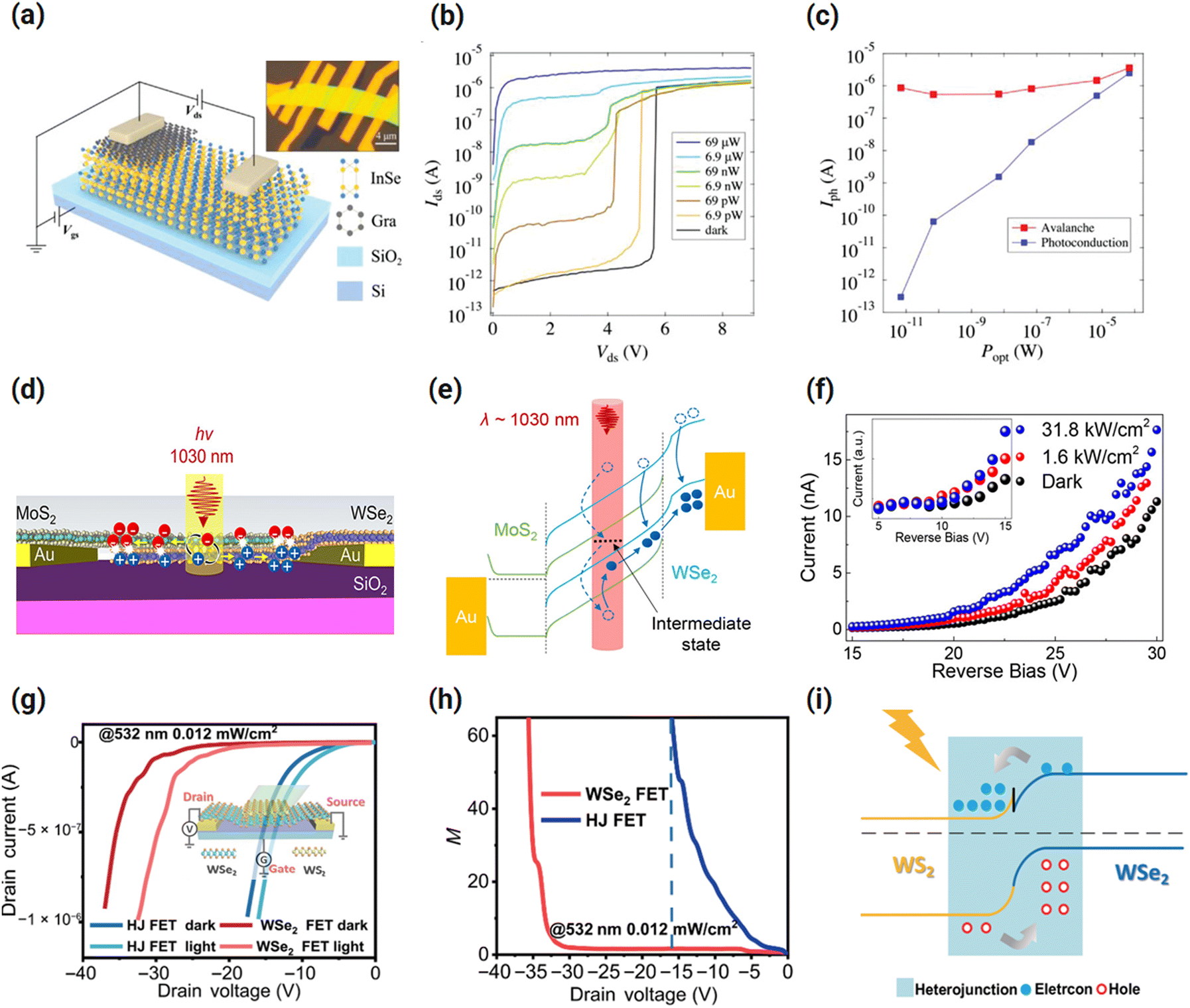 | ||
| Fig. 7 (a) Schematic illustration of the APD: inset represents the optical image of the fabricated APD. (b) IDS–VDS characteristic curves were examined with different laser powers (6.9 pW–69 μW). (c) Iph of the avalanche mode at VDS = 5.5 V (red curve) and photoconductive behaviour at VDS = 2 V. Figures (a)–(c) are reproduced with permission from ref. 101, copyright, Advanced Materials (2022). (d) Schematic of an avalanche photodiode based on WSe2/MoS2. (e) Schematic of the band diagram of the TPA APD representing the carrier transport in the avalanche state. (f) I–V characteristics of the photodiode in avalanche mode, measured in darkness (black) and under illumination at two distinct optical power densities: 1.6 kW cm−2 (red) and 31.8 kW cm−2 (blue). The inset illustrates an enlarged type of I–V curve, evidently revealing photocurrents at a substantial reverse bias facilitated by the significant avalanche “G”. Figures (d)–(f) are reproduced with permission from ref. 117, copyright, Nano Letters 2022. (g) I–V characteristics of the WSe2 FET and HJ FET under dark and exposure to light. (h) Gain (M) of two devices. (i) Band structure of the heterojunction WSe2/WS2. Figures (g)–(i) are reproduced with permission from ref. 116, copyright, Nano Research 2023. | ||
5.2. TMDC heterostructures based on avalanche photodetection
The photodiode consists of a monolayer of MoS2 and a monolayer of WSe2, with a vdW heterostructure reported.117 Stable 2D materials like MoS2, WS2, and WSe2 are greatly sought for infrared photosensors. Nonetheless, many materials include bandgaps inside the visible spectrum, hence limiting their sensitivity to infrared photons.97,171,172 A multiphoton absorption technique may facilitate the detection of infrared photons by 2D materials with substantial bandgaps.173 The two-photon absorption (TPA) development has been used to create infrared photodetectors based on 2D materials due to the substantial TPA coefficients174 relative to higher-order nonlinear processes.175,176 However, the TPA-based nonlinear method is very inefficient, resulting in poor “R” for TPA photodetectors using 2D materials.177,178 We reviewed here effective 2D material-based TPA photodiodes that attain significant R via the use of the avalanche multiplication phenomenon. Fig. 7(d) depicts the 3D schematic of the proposed TPA-APD. The photodiode consists of a monolayer of MoS2 and a monolayer of WSe2, with a vdW heterostructure area situated between them. The p–n junction is established in the WSe2/MoS2 heterostructure due to WSe2 being an inherent p-type semiconductor and MoS2 being an intrinsic n-type semiconductor.179 For the one- and two-photon absorption studies, a continuous-wave (CW) 532 nm laser and a pulsed 1030 nm laser are utilized, respectively. Photogenerated electrons and holes undergo multiplication in MoS2 and WSe2 monolayers, correspondingly, by the avalanche multiplication phenomenon. Fig. 7(e) illustrates the energy band configuration, representing TPA-based optical absorption and carrier multiplication during transit. Because the energy of the excitation photon is less than the bandgap energies of both MoS2 and WSe2, holes (electrons) in the conduction band (valence band) must absorb two photons to be elevated to the valence band (conduction band).180 In WSe2, photoexcited holes are amplified during transit by the avalanche effect, but in MoS2, photoexcited electrons undergo multiplication. Fig. 7(f) displays the I–V characteristics of the TPA-based APD under both dark conditions and under 1030 nm light. The TPA process is fundamentally weak, resulting in a negligible photocurrent even at a substantial optical power density of 31.8 kW cm−2 when the reverse bias is less than 10 V, as seen in the inset image of Fig. 7(f). The enhanced avalanche effect at high reverse biases enhances the R by about three orders. This study demonstrates unprecedented R, attributable to both a high two-photon absorption coefficient and a substantial avalanche G in monolayer MoS2 and WSe2. The rapid charge transfer mechanism of photogenerated charge carriers in the heterostructure area may enhance R. Here we have reviewed another power efficient WSe2 avalanche photodetector designed using an in-plane WSe2 FET and an out-of-plane WSe2/WS2 P–N junction. The decreases in breakdown voltage (Vb) in the HJ-FET are seen and the greater “R” in the HJ-FET is explored under light exposure. Fig. 7(g) presents the I–V curves of the WSe2 FET and HJ FET under dark and light modes: inset illustrates the schematics of the APD. Both kinds of devices represent an enhanced current and decreased breakdown voltage under 532 nm laser light and the highest R is 135 A W−1. Fig. 7(h) illustrates the G in both kinds of samples. It is clearly shown that the HJ FET has greater gain with respect to the same VDS when the bias is in the range of −5 to −16.5 V. Furthermore, the maximum G over 60 is observed in both types of devices. Fig. 7(i) shows the band structure of the WSe2/WS2-based structure, which denotes the movement of charges after illumination. These outcomes indicate that the use of the WSe2/WS2 heterostructure is a substantial way to improve the efficiency of APDs with low power utilization.1166. 2D-hybrid heterostructure based on avalanche FETs
6.1. Plasmonic waveguide (APD)
Silicon photonics181 has emerged as a viable platform for several significant applications including on-chip optical sensors,182 optical telecommunications183 and nonlinear photonics.184 We reviewed here a high-speed and very sensitive device based on Si/BP hybrid plasmonic waveguide (HPWG) APDs effective at the wavelength of 1.55/1.95 μm. The HPWG on a thin silicon-on-insulator (SOI) platform is specifically designed to augment light absorption by the BP while concurrently facilitating brief carrier transit times, which is crucial for attaining high speed and high “R” in the photodetector. Fig. 8(a) illustrates the graphic architecture of the current Si-BP HPWG-based APD combined with various passive components, with the two-channel (1.55/1.95 μm) wavelength-division (de)multiplexers and the grating couplers at the input/output terminals. These passive parts are implemented to effectively characterize the current devices operating throughout a wide wavelength range, considering that a grating coupler is typically wavelength-sensitive and has a restricted operational bandwidth of around several tens of nanometers. In the active area, a horizontal Si-HPWG is introduced, including double nano-slots flanking a central silicon core and two metal strips on each side.185,186 The horizontal HPWG is specifically enveloped by a multilayer BP sheet, as seen in Fig. 8(a) and (b), therefore augmenting light absorption in the BP layer. The two metal strips function as source (S) and drain (D) electrodes, therefore minimizing the transit distance between them to enhance reaction speed. The “Si” core and the BP layer are physically separated by an ultrathin Al2O3 insulating layer. Instead of using the usual Si with a thickness of 220 nm, a thin Si-core was employed to increase light absorption by the BP.187 The exfoliated BP film is successfully floated above the nanoslots within the electrodes and the Si-core due to the exceptional mechanical characteristics of the BP flake.185 The study indicates that raising the thickness of the BP layer enhances its optical absorption.188 Conversely, a thinner BP layer is favoured to get reduced mode-mismatching loss and enhanced mobility,189 which is crucial for obtaining a rapid response. A modest BP thickness (about 30 nm) is used for the existing photodetector to optimize the balance between R and speed. Furthermore, due to the anisotropic nature of BP, its orientation significantly influences the electrical and optical characteristics of the photodetectors.190 The biasing is established to remain below 2 V to prevent thermal breakdown. Fig. 8(c) illustrates the recorded photocurrent of the current BP photodetector functioning at a 1.95 μm wavelength. The optical power ranges from 1.4 to 186 μW. The photocurrent has a behavior similar to that of the dark current, demonstrating a superliner growth at elevated voltages. The photocurrent exhibits a quick increase at low optical power levels (e.g., <15 μW) and then rises more gradually as the optical power ascends to 186 μW. R significantly rises, attributed to the space charge effect, a phenomenon extensively reported in fundamental APDs.191 Increased photocarrier densities resulting from greater optical power diminish the E-field strength inside the multiplication area. In the coming times, electrical bandwidth may be improved by reducing the gap between both electrodes, while the dark current can be minimized by properly regulating the height of barrier. In comparison to previously reported photodetectors, the current Si/BP HPWG based APD is among the most superior devices, offering a potential alternative for future optical applications. | ||
| Fig. 8 (a) Schematic arrangement of the device-based Si/BP. (b) SEM image of the fabricated device. (c) The examined photocurrent of the APD as the bias varies. Figures (a)–(c) were reproduced with permission from ref. 216, copyright ACS Photonics (2022). (d) Schematic representation of the energy band configuration of WS2/Bi2O2Se under light exposure. (e) The photocurrent of the FIP with various intensities (650 nm) may be categorized into three distinct zones: the normal reverse bias effective zone (I), the avalanche breakdown zone (II), and the reverse bias breakdown zone (III). The red circles indicate the avalanche “G” achieved at a light intensity of 56.7 μW. (f) The photoresponse of the device at 1550 nm, with intensity (0 mW to 7.0 mW) is revealed, with the red circles indicating the avalanche “G” of the device under 1550 nm light at 7.0 mW. Figures (d)–(f) were reproduced with permission from ref. 217, copyright, Optics Communications (2023). (g) Working phenomena and avalanche multiplication behaviour of nMAG/Si APD are illustrated schematically. (h) Dark and photocurrent inspection in the avalanche region. (i) “G” at different power intensities of radiant light as a function of reverse biasing. Figures (g)–(i) are reproduced with permission from ref. 218, copyright, Advanced Optical Materials (2024). | ||
6.2. Broadband fiber-integrated APD of WS2/Bi2O2Se
Layered bismuth oxychalcogenide (Bi2O2Se), a recently identified 2D material, exhibits exceptional mobility (∼20000 cm2 V−1 s−1), a suitably slight band gap of 0.8 eV, and outstanding air stability, thus positioning it as an outstanding contender for optoelectronic devices.192,193 WS2 has garnered significant scientific attention due to its exceptional optical characteristics, particularly in the domains of sensors and photonic devices.194,195 The inadequate efficiency of Bi2O2Se-based photodetectors is attributed to elevated dark current and a diminished ON/OFF ratio while restricting light absorption due to the poor responsivity of pure WS2.196,197 Assembling vdW heterojunctions has been described as an active technique to resolve the issue of high dark current and to adjust interlayer transition energy. The bandgap of Bi2O2Se is 0.8 eV, whereas WS2 has an indirect bandgap of 1.38 eV, enabling the formation of a type-II vdW heterostructure between 2D WS2 and Bi2O2Se.192,198,199 We review a self-powered high-speed fibre-integrated photodetector (FIP) based on the WS2/Bi2O2Se heterostructure on the end face of the optical fibre. This FIP operates in the avalanche zone, exhibiting an EQE of 141% and a “G” of 44. Notably, this FIP has strong performance in wrist bending measurement, indicating significant potential motion recognition application alongside traditional photodetection. The conduction band energies of WS2 and Bi2O2Se are 4.5 eV and 4.25 eV, correspondingly.200,201 The Bi2O2Se electrons will migrate to the WS2 side due to different Fermi levels. Consequently, a type II band configuration is established at the junction of the overlapping WS2/Bi2O2Se as seen in Fig. 8(d), accompanied by the emergence of a built-in E-field in the depletion region. The limited band gaps of WS2 and Bi2O2Se facilitate the absorption of a greater number of incoming photons. Fig. 8(e) illustrates the device's photo-response measured under dark and light at a λ of 650 nm with varying power of incident light. Even when the applied bias surpasses 80 V, the dark current remains significantly low. Conversely, with an applied bias below 39 V (region I), the photocurrent rises gradually; however, it escalates significantly when the bias voltage exceeds 39 V owing to the avalanche effect. In Fig. 8(e), the critical device parameters are presented at a bias of 68 V (area II), and the R, EQE and G are calculated to be 0.74 A W−1, 141%, and 44 under a power intensity of 56.7 μW. Moreover, at a bias of 80 V (region III), the EQE attains 642% with an improved R of 3.36 A W−1 at incident light with the power of 5.2 μW. The elevated EQE above 100% is ascribed to collisional-ionized carrier multiplication. Additionally, the distinguishing feature of APDs is investigated, which shows a linear relationship between the incident power of light and photocurrent response at different biases. The APD of FIP is wideband; meanwhile, the avalanche effect is distinct at 1550 nm of incident light (Fig. 8(f)). The avalanche effect was seen under a bias voltage above 32 V. Upon increasing the biasing voltage up to 46 V, reverse bias breakdown commenced. The amount of photocurrent was minimal at bias voltages below 32 V at a wavelength of 1550 nm. The photocurrent rose quickly as the bias voltage increased. The photocurrent reached 148 μA with a G of 12.88 when the illumination intensity was 7.0 mW and the bias voltage was 60 V. This “FIP” has excellent capabilities in measuring bending deformation due to its great sensitivity to variations in light intensity. A reliable method to produce rapid, broadband fibre-integrated photodetectors is provided by this work, which has potential uses in fibre-integrated multifunction systems.
6.3. Self-quenched avalanche photodetectors
There have been many recent reports on APDs based on III–V compound semiconductors, silicon (Si), and germanium (Ge).202–204 Because of their small bandgap characteristics, APDs constructed from Ge and III–V semiconductor materials have been extensively used for sensing in the near-infrared (NIR) band.102 Nevertheless, these APDs' hole–electron dissociation ratio (k-value) is almost “1”, which leads to a significant amount of extra noise that makes it challenging to improve the device's efficiency even further.205,206 Si electronic components are perfect for achieving high carrier multiplication because of their very low k-value (<0.1), low dark current, and superior multiplication capabilities.207 Consequently, enhanced Si-based APDs that allow for sensitive NIR spectrum detection are needed, especially in the communication band. The most appropriate method for achieving this is to develop a heterojunction APD by combining a 2D material with Si, which can increase the operational bandwidth that goes beyond the communication band. Graphene has special properties including durability, small band gap, and greater carrier mobility and acts as a significant 2D material.208 High-performance photodetectors may benefit from macro-assembled graphene nanofilms (nMAG) because of their large-area, high crystallinity, and precisely controlled thickness.209 We reviewed here a vertical heterostructure photodetector made of nMAG and epitaxial silicon (epi-Si) with an R of 0.38 A W−1 and a response time of 1.4 μs. Additionally, the APD shows a very low noise level and a significant avalanche G of 1123. In addition to enabling self-quenching by switching from light to dark via avalanche multiplication, it can operate with relatively smaller avalanche turn-on voltages and transfer data at a real-time rate of 38 Mbps over data networks for near-infrared light communication. The suggested structure makes it possible to use complementary metal-oxide-semiconductor (CMOS) compatible methods to fabricate high-performance APDs in the infrared spectrum. The schematic diagram of an APD is presented in Fig. 8(g); when the bias voltage is raised, the nMAG layer turns as the absorption layer for the NIR longwave spectrum in the nMAG/epi-SI device, as presented in Fig. 8(g). The mildly doped epi-Si layer, conversely, functions as a multiplication layer. Electrons are driven into charge multiplication zones in epi-Si by the provided reverse bias, which also separates photon-generated electron–hole pairs. Photogenerated electrons gain significant kinetic energy under an extensive internal electric field in a relatively large depletion region, and avalanche multiplication can be accomplished through impact ionization with valence electrons in the lattice, resulting in free electrons that grow exponentially, causing the rapidly increasing photocurrent. In epi-Si, phonon concentration rises with temperature, leading to rapid energy loss through electron–phonon collisions. Therefore, carriers can only acquire the energy needed for impact ionization and avalanche multiplication in greater electric fields. The I–V graphs in Fig. 8(h) show that when the voltage reaches a particular threshold, the current rises quickly. As the power density varies from 0.11 to 1.14 W mm−2 (see the inset of Fig. 8h), the breakdown voltage (Vbr) gradually drops from −13.5 to −11.9 V, which is much lower than the dark current (−23.7 V). Since the high-power density increases the number of nMAG-excited photogenerated carriers, which enables early impact ionization of electrons, the change in threshold voltage enhances the avalanche multiplication effect. Additionally, an unequal resistance distribution brought about by the high-power density increases the influence of ionization gain and the electric field on nMAG.210 The self-quenching action of the device is very beneficial in protecting APDs from damage caused by high current densities. The illumination-dependent Vbr allows the nMAG/epi-Si photodetector to perform avalanche self-quenching. It was established that the device's avalanche voltage is greater when it is not lighted than when it is, according to the results shown in Fig. 8(h). The avalanche breakdown will begin at 1550 nm with 0.11 W mm−2 illumination if the operation voltage is adjusted to −13.5 V. However, when there is no light present, the device's avalanche voltage rises to −23.7 V. When the device is not lighted and the breakdown voltage exceeds the operating voltage, the avalanche breakdown within the device will automatically quench, causing the current to drop rapidly. The self-quenching mechanism used in the nMAG/epi-Si photodetector protects against operational failures, increasing its longevity. The avalanche multiplication mechanism in this device is activated only by incident light, but only if the operating voltage is improved to a critical point. These findings show that avalanche multiplication dominates the internal benefit. The gain of 1123 (Fig. 8(i)) is calculated employing the equation M = Iph/Iph0 at a low reverse bias, where Iph and Iph0 are photocurrents with and without multiplication, correspondingly. Because of the avalanche effect, the nMAG/epi-Si photodetector displays outstanding performance when equated with the previous research results, including a low dark current, high responsivity, and detectivity, as well as a fast response time.211–215 Additionally, the photodetector has been successfully employed to record pictures and may be used for dual-colour detection. This work offers recommendations for the design of NIR image sensors and optical communication devices based on 2D/Si heterostructures.7. Avalanche FET application in bio-sensing phenomena
7.1. Avalanche regulation in a bionic transistor
Visual adaptive devices provide the capacity to streamline circuits and processes in machine vision structures, enabling adaptation and perception of photos under diverse brightness conditions; nevertheless, this capability is constrained by a slow adaptation process. Here, we review avalanche modification as feedforward inhibition in bionic 2D transistors to achieve high-frequency visual adaptation with perceptual accuracy at the microsecond level, attaining a response speed that is over 10000 times more rapid than that of current bionic sensors and the human retina. To enable ultra-fast scotopic and photonic adaptation processes of 108 μs and 268 μs, as well, the bionic transistor autonomously transitions between avalanche and photoconductive effects in response to changes in light intensity. An adaptive machine vision system was developed by combining convolutional neural network technology with avalanche-based bionic transistors. It demonstrates remarkable microsecond-level speed adaptation and reliable image recognition with 98% accuracy under both low and intense light conditions. Fig. 9(a) presents the graphical illustration of the reviewed device structure. This junction-FET (J-FET) consists of a MoS2 transport channel and a WSe2 gate. Fig. 9(b) shows how the incident light stimulus may greatly alter the output current and avalanche mechanism. As incident light intensifies, it causes an increase in the photocurrent, exhibiting positive photoconductivity (PPC) in both the saturation and linear zones; but, in the ionization region, the PPC progressively shifts to negative photoconductivity (NPC). The photocurrent first rises to 5.1 μA and thereafter declines to −2.2 μA as light strength increases, resembling spontaneous visual adaptation that mitigates the output of overstimulation information. The avalanche “G” decreases from 1.5 × 10⁴ to −8 as light intensity rises, indicating a shift from the avalanche to the photoconductivity effect as the major photo-sensing mechanism. The R in the ionization zone undergoes substantial variations in both value and polarity, ranging from 7.6 × 10⁴ to −1 × 10³ A W−1, but in the saturation zone, it fluctuates little from 158 A W−1 to 5 A W−1. The sensitivity progression in the ionization area parallels that in the retina, hence affirming the device model's credibility.219 The IDS exceeds the leakage current by over 103, validating the avalanche effect and demonstrating the device's great steadiness. In the human retina, transitioning from dim to bright environments results in the alternating dominance of photoreceptors, specifically rod cells (high sensitivity) and cone cells (low sensitivity), in perceptual function. The transformation from rod to cone cells in the retina is analogous to the switch between avalanche and photoconductivity effects in a device. In this order, the J-FET has been given visual behaviour by the avalanche tuning under different light illumination circumstances. Because of this, the retina's sensitivity progressively alters over time throughout a protracted process of visual adaptation. Feedback inhibition and regeneration/bleaching of the photopigment govern the photoreceptor cell's transition.220,221 In contrast, the device sensitivity development in the avalanche ionization area is light-adaptive and real-time, guaranteeing the user quick detection of environmental changes and preventing any possible injury from the human retina's protracted scotopic and photopic adaptation process. The changeover of the photo-sensing mechanism is reported to be accompanied by sign reversal and magnitude variations with more than five orders of R and avalanche G. In comparison to the retina and the reported bionic device with visual adaptation, a significant distinction in sensitivity at weak and strong light stimuli may aid in imagining contrast improvement. Upon associating the R and G with previously tested APDs, this device exhibits exceptional APD characteristics, featuring a G of 1.5 × 10⁴ and R reaching 7.6 × 04 A W−1, indicating significant potential for weak-light detection and enhanced visualization in low-light environments, functioning as a bionic visual sensor.59,100,116,117,141,222,223 As seen in Fig. 9(c), this device, in contrast to other 2D bionic devices, could improve optical adaptation beyond the retina by providing an effective bionic neural network. The avalanche effect's photosensitivity is four orders of magnitude more than that of the photoconductivity effect, which means that it may mimic the roles of rod and cone cells in this network. The photogenerated voltage opposes the direction of the built-in E-field at the MoS2/WSe2 junction, functioning as an inhibitory cell that modulates the avalanche effect. Light (stimulation), “Photo-generated voltage” (Inhibition cell), and “avalanche” (Rod) may establish a feedforward inhibitory circuit in which the “avalanche” gets both stimulatory and inhibitory signals to prevent excessive output under photopic adaptation circumstances. Under intense light irradiation, the avalanche effect is suppressed, transitioning the photo-sensing process to “photoconductivity” (Cone). The transition between “photoconductivity” and “avalanche” during both photopic and scotopic adaptation occurs far more rapidly than the chemical reaction-based switching between cones and rods in the retina. The feedforward excitation circuit including the “Output current,” “avalanche,” and “photoconductivity” demonstrates multiplexed modulation properties and significantly enhances the “SNR”. This device offers significant benefits in photographic adaptation over the human retina and previously described bionic devices by using a feedforward circuit as a rapid-switching phenomenon. By using a more predictive and quick feedforward inhibition circuit, the avalanche tuning-based bio-inspired visual device can avoid prolonged visual adaptation. This has great potential for wide-ranging machine vision applications, promoting concepts and schemes for bio-inspired optical systems while reducing reliance on intricate systems and computation.
 | ||
| Fig. 9 (a) Graphical illustration of the device. (b) I–V of the device under illumination with Vgs = −3 V. (c) Schematic of the bionic neuronic system; red circles denote the circuit themes. Figures (a)–(c) are reproduced with permission from ref. 241, copyright, Nature Communications 2024. (d) Schematic of the MoS2−xOx-based gas sensing device. (e) Vb and “α” with VDS = 35 V at VGS = 20 V revealed in the form of balls and squares, correspondingly. Figures (d) and (e) are reproduced from ref. 242, (2024). (f) Energy band diagram. (g) The carrier transport phenomenon inside the device. (h) The arithmetic simulation calculated the current-reverse bias with various functional strains; the inset shows the schematic illustration of a piezotronic GaN avalanche device. (i) The (IDS–VDS) curves of the reverse breakdown in an FET in the presence of piezoelectric charges. Figures (f)–(h) are reproduced from ref. 243, copyright, Nano Energy. | ||
8. Avalanche FET application for gas sensing
8.1. NO2-gas sensing in doped-MoS2
Recently, avalanche multiplication has been seen in TMDCs such as MoS2 and various other 2D-TMDC materials, attributed to robust Coulomb interaction-induced quantum confinement effects.117,224 Operating TMDC-based FETs in an avalanche multiplication mode via gate-voltage tuning allows for the amplification of weak signals generated by light or molecular adsorption. An enhanced signal via avalanche multiplication demonstrates reduced background noise and extreme sensitivity, allowing detectors to attain outstanding performance.97,101 In order to achieve outstanding sensing efficiency, there is a growing push to improve and make use of carrier multiplication phenomena for gas sensing. Nearest-neighbour hopping (NNH) is a prevalent occurrence in materials with higher defect concentrations, facilitating the production of greater carrier concentrations in defective substances.225–227 In order to tackle this challenge, the research looks into avalanche multiplication in MoS2 with high defect concentrations. The impact of NNH on the effectiveness of MoS2 avalanche multiplication is clarified in this work. By substituting oxygen (O) atoms for sulphur (S) atoms in a monolayer of MoS2, the defective configuration is generated as referred to as MoS2−xOx, with x meticulously regulated between 0 and 0.51. When x surpasses 0.44, significantly doped O defects allow MoS2−xOx to demonstrate NNH. While maintaining MoS2-like carrier mobility, the presence of O defects in MoS2−xOx increases the possibility of carrier collisions compared to pure MoS2. Additionally, a gas sensor was constructed that exploits the avalanche multiplication properties of MoS2−xOx. This sensor (MoS2−0.51O0.51) possesses a limit of detection (LOD) of almost 1.4 × 10⁻⁴ ppb and demonstrates an outstanding gas response to 50 ppb NO2 at ambient temperature, achieving an impressive signal R of 5.8 × 10³%, exceeding conventional resistance-type gas sensors utilizing TMDCs by two times. The MoS2−xOx gas-sensor FETs function using avalanche multiplication features, in contrast to traditional detectors that use two parallel electrodes for gas ionization and breakdown voltage assessment.228–231 The monolayer MoS2 utilized in this work is produced by the CVD method. Following treatment, O atoms replace S vacancies, resulting in the O doping of the irradiation film designated as MoS2−xOx, as seen in Fig. 9(d): the inset shows the optical image of the device. Upon exposure to NO2 gas, the sensor continues to demonstrate avalanche multiplication behaviours, with the breakdown voltage (Vb) rising from 13.8 V to 21.8 V as the gas amount escalates from 50 ppb to 200 ppb, while the “α” decreases from 954.5 cm−1 to 669.8 cm−1 (Fig. 9(e)). Simultaneously, the IDS of the MoS2−0.51O0.51 based FET reduces by two orders of magnitude in the avalanche zone (VDS > Vb). In comparison to the MoS2 FET, the MoS2−0.51O0.51 FET shows a substantial sensitivity to NO2 gas, as shown by the much greater IDS change. The O-substituted configuration is linked to the anticipated transfer of charge of the NO2 molecule at the adsorption location. During adsorption, NO2 removes electrons from the MoS2−0.51O0.51 surface like that of adsorption on the MoS2 layer. MoS2−0.51O0.51 presents n-type semiconducting behaviour; hence its carriers are exclusively electrons. The adsorption of NO2 on the MoS2−0.51O0.51 surface diminishes the carrier density of MoS2−0.51O0.51. This sensor is adaptable and appropriate for detecting gas concentrations, especially at low levels, since it does not need precise gas pressures. This work highlights avalanche multiplication as a successful physical mechanism for the development of ultrasensitive gas sensors and shows how to modify its characteristics using hopping transfer.9. Piezotronic and piezophototronic avalanche devices
The piezotronic effect may be exploited to fabricate robust devices based on avalanche multiplication. Avalanche devices, such as single photon avalanche diodes (SPADs), employ nonlinear current amplification to detect single photons.80,232 SPADs respond in 10−12 s, whereas standard photomultiplier devices respond in 10−9 s.233 The maximal G factor and VEB of SPADs are critical factors that may be improved by altering the device's architecture,234 building heterojunctions by switching materials235–237 and improving interface polarization using dopants. The vertical conductive configuration of the p–n diode, which had a critical breakdown E-field of 3.5 MV cm−1 and a breakdown voltage of 2600 V, served as the basis for GaN avalanche devices.238 The GaN avalanche device was theoretically investigated by means of the finite element approach, as we reviewed here. The strain-induced polarisation controls the avalanche process. This refers to the impact of piezotronic and piezophototronic processes on single-photon avalanche diodes that are extremely quick and sensitive. Because strain-induced polarisation can efficiently regulate the carrier's transit at the interface, piezotronic strain sensors offer extremely high sensitivity. Both centrosymmetric materials with non-uniform strain and non-centrosymmetric materials, such as wurtzite-structured semiconductors like ZnO, GaN, etc., can be used to create piezotronic devices. Under reverse bias, the piezotronics-MOSFET breakdown model was constructed. Under various strains, the current–voltage characteristics were computed. Polarization brought about by strain amplifies the current in the depletion layer. It is evident that both the gauge factor and the breakdown time can be improved. It is possible to greatly enhance the efficiency of piezotronic and piezophototronic avalanche diodes. The perfect p–n junction design is applied to the avalanche diode in accordance with Shockley's theory. Carriers smash through the barrier area at high reverse bias voltages. In a sufficiently large space charge region, the covalent bond's electrons are energized to produce a free electron–hole pair. Fig. 9(f) displays the E-field and charge; ionization will result from the acceleration of the free carriers in the depletion area and their collision with the lattice atoms under the strong E-field. The impact ionization process creates free electron–hole pairs. When the reverse current rises quickly as an effect of the multiplication, breakdown occurs. At the time of the avalanche collapse, the depletion layer becomes wider. The characteristics of the depletion layer determine the avalanche breakdown conditions.239 Fig. 9(g) shows the GaN piezotronic avalanche device schematic construction and carrier transport. In earlier studies, the strain was used to efficiently control the piezoelectric polarization charges at intersection.240 The strain direction determines the direction of charges; piezoelectric charges have a width of Wpiezo. The piezotronic device has been investigated using a 2D strained model that incorporates the p-type area and n-type zone with piezoelectric charges in order to get a detailed understanding of the piezotronic and piezophototronic impacts on the avalanche development. The electric field scenarios are described by ideal Ohmic connections and Dirichlet boundary conditions. The inset of Fig. 9(h) displays the piezotronics avalanche diode schematic. Within the width Wpiezo, the piezoelectric charges are dispersed at the n-type zone of wurtzite GaN. The reverse voltage is fixed at V = 4 V and the uniform strain varies from −1 to 1%; the current voltage characteristics are displayed in Fig. 9(h). The current increases gradually at first when the reverse voltage rises, and the speed clearly improves as the voltage rises. The current progresses with the externally functional strain for a given reverse voltage, particularly when it is close to the breakdown voltage. The piezotronic polarization field gives the avalanche process an alternative starting point. Positive and negative piezoelectric charges are produced by the applied strain in distinct directions. Eventually, the device breaks down due to the rising drain–source voltage. Fig. 9(i) displays the current–voltage characteristics for IDS and VDS at various stresses. The applied strain causes the current to rise at a constant voltage. It is clear that the MOSFET at 0.02% strain generates carriers more quickly than the other one. It is described how the avalanche mechanism controls the piezoelectric electric field. The gauge factor can reach up to 106–107, and the device has extremely high sensitivity. Previously, the voltage was employed to regulate the critical state of the classic avalanche device; today, the external strain is controlled. The link between carrier transport and piezoelectricity in the junction zone also clearly reduces the reaction time. For ultrafast and ultra-high sensitivity piezotronic and piezophototronic strain sensors, which have enormous potential applications in biosensing and human–computer interfaces, the study has considerable guiding importance. It is also evident that the connection between carrier transport and piezoelectricity in the junction zone shortens the response time. The discovery has significant implications for ultrafast and ultra-high sensitivity piezotronic and piezophototronic strain sensors, which have vast potential applications in biosensing and human–computer interfaces.10. Challenges, solutions and future perspectives
The avalanche transistors are typically operated in a certain phase where they deliberately endure an avalanche breakdown. This distinct mode experiences high voltages and switches rapidly, but it also faces a set of challenges. However, the fundamental problems for the avalanche breakdown phenomenon are the fabrication strategy and integration of high-quality 2D materials onto FET architectures.247 So far, sustaining the crystalline integrity, consistency, and scalability of these materials has remained an issue for circuit integration and limited power. The quality of the interface between 2D materials and substrates is also critical for device performance. The defects, residue, or incompatible interfaces may result in suboptimal electrical performance or device instability.248 The avalanche FETs inherently depend on regulated avalanche breakdown; attaining an equilibrium between substantial gain and low noise without compromising the device is technically demanding.249 Therefore, the quantum engineering of materials and device configurations at the nanoscale level are essential to mitigate the random behaviour of the avalanche process. This would help to control the heat dissipation effect during avalanche multiplication in the channel materials.250,251 The 2D materials have good conductivity, but still, the voltage overshoot, optical crosstalk and reliability under high stress can cause the breakdown voltage drift, which can potentially damage the devices. In addition, avalanche FETs should sustain a high “SNR” for practical sensing applications. Reducing noise and maintaining uniformity may be technically indispensable for advanced real-world applications.252,253 Long-term stability and performance reliability are essential for commercial sensing applications. Moreover, ensuring the reliable and stable operation of devices over a long period under diverse environmental conditions (temperature and humidity) is a major challenge for 2D-based avalanche FETs.254,255 The 2D materials are susceptible to environmental deterioration, such as oxidation in the atmosphere, which may impair their performance.256,257 Despite all, the promising electrical transport features of 2D materials have significant potential in sensing applications.258,259 Owing to their extensive surface area and electrical characteristics, 2D materials can achieve high sensitivity and selectivity for various analytes (e.g., gases and biomolecules).260,261 Further to enhance the performance of the devices it is essential to develop ultrahigh-efficiency avalanche devices for various applications in optical communications, biomedical imaging, and green energy. Protection solutions, including encapsulation, should be devised without impairing device performance. Ongoing investigation for innovative 2D materials and their heterostructures may provide unique advantages for avalanche FETs. The ongoing investigation of various materials beyond graphene, such as h-BN, BP or hybrid organic-2D systems, may provide distinct benefits for bandgap engineering, breakdown voltages, and electrical characteristics. Employing novel manufacturing processes, including CVD, MOCVD,262 atomic layer deposition (ALD), and molecular beam epitaxy (MBE), can enhance the quality and scalability of 2D materials, which may pave the way for the future of avalanched FETs. Also, the advancements in transfer systems and the incorporation of 2D materials with current silicon-based technologies will be crucial for the progression of avalanche FETs. Avalanche FETs using 2D materials may become essential for next-generation sensors in IoT applications, environmental monitoring, and healthcare diagnostics. The distinctive characteristics of 2D materials render them ideal for the detection of gases and biomolecules with unparalleled sensitivity and reaction times.Avalanche transistors demonstrate a groundbreaking and robust approach to the development of multifunctional devices, making them a promising frontier for modern and fast electronics of next-generation. Recently, 2D materials have become an ideal contender for future soft electronics, facilitating diversity in high-frequency and high-power applications.263–265 The avalanche effect by impact ionization can be exploited to establish novel technologies in optical, chemical and bio-sensory applications. Such sensors could be connected with healthcare, real-time diagnostics, and environmental monitoring. Also, the optimization of APD performance can lead to devices with enhanced performance as compared to traditional avalanche designs by selecting 2D materials with promising band alignments and structures that allow for the use of Schottky junctions to reduce dark currents and increase operational wavelengths under light. In the future, the machine learning and integration of antifouling technology may be linked with avalanche FET-based sensors to augment data processing and in vitro and in vivo diagnostics. With the advancement of 2D material-based avalanche FETs, industries such as electronics, healthcare, environmental monitoring, and defence could see a significant shift in sensor technology. High-performance, low-power, and miniaturized sensing devices could open new possibilities in industrial automation, smart cities, and more. By mitigating the current issues in both material and device designs, the future of avalanche FETs using 2D materials seems auspicious for advanced sensing applications.
11. Conclusion
In this review, we thoroughly discussed the mechanism and recent progress of avalanche transistors especially manifested by 2D materials. In addition, we explored the emerging developments in photo-, bio- and gas sensing applications employing avalanche photodetectors/photodiodes (APDs). Also, it is concluded that the 2D materials offer novel approaches for the advancement of APDs due to effective carrier multiplication at the nanoscale, which potentially facilitates their scope in soft wearable sensors, organ-on-a-chip applications and cell-based sensors for drug screening. Such integration of 2D materials into avalanche FETs marked significant progress in advanced detection technologies of the contemporary era. Finally, we highlighted the challenges of avalanche transistors and their possible solutions to compete in the race of advanced sensing technology. Furthermore, we provided our future perspectives on 2D material-based avalanche FETs regarding material selection and device configuration. However, many challenges and principles are elusive, so we expect that the incorporation of 2D materials in superjunction MOSFETs also paves the way for high-frequency driving photocathodes of fast-gating image intensifiers.Author contributions
E. E. and MFK: writing – original draft, reviewing and editing; J. A. and U. A.: validation; P. C. and M. A. A.: visualization; K. J. S. and U. A.: proofread the manuscript; and Z. S.: supervision and funding acquisition.Conflicts of interest
There are no conflicts to declare.Data availability
No primary research results, software or code have been included and no new data were generated or analyzed as part of this review.Acknowledgements
Zdenek Sofer was supported by the ERC-CZ program (project LL2101) from the Ministry of Education Youth and Sports (MEYS). The authors acknowledge the assistance provided by the Advanced Multiscale Materials for Key Enabling Technologies project, supported by the Ministry of Education, Youth, and Sports of the Czech Republic. Project No. CZ.02.01.01/00/22_008/0004558, Co-funded by the European Union. This work was supported from the grant of Specific university research – grant No A1_FCHT_2025_013. K. J. S. was supported by the Johannes Amos Comenius Programme, European Structural and Investment Funds, project CHEMFELLS VI (no. CZ.02.01.01/00/22_010/0008122). The authors extend their appreciation to the Deanship of Research and Graduate Studies at King Khalid University, Saudi Arabia, through Large Research Project under the grant number RGP-2/673/46.References
- M. Kim, M. Suleman, N. Nasir, H. M. Park, S. Lee, E. Elahi, H. Noh, S. Kumar and Y. Seo, Nano Energy, 2025, 110687 Search PubMed.
- H. Yuan, Y. Huang, T. Gong, Y. Wang, P. Jiang, W. Wei, Y. Yang, J. Chai, Z. Wu and X. Wang, IEEE Electron Device Lett., 2024, 45(12), 2371–2374 CAS.
- E. Elahi, M. F. Khan, S. Rehman, H. W. Khalil, M. A. Rehman, D.-K. Kim, H. Kim, K. Khan, M. Shahzad and M. W. Iqbal, Dalton Trans., 2020, 49, 10017–10027 RSC.
- E. Elahi, G. Dastgeer, A. S. Siddiqui, S. A. Patil, M. W. Iqbal and P. R. Sharma, Dalton Trans., 2022, 51, 797–816 RSC.
- M. W. Iqbal, S. Razzaq, N. Noor, S. Aftab, A. Afzal, H. Ullah, M. Suleman and E. Elahi, J. Mater. Sci.: Mater. Electron., 2022, 33, 12416–12425 CrossRef CAS.
- M. F. Khan, E. Elahi, N. U. Hassan, M. A. Rehman, H. W. Khalil, M. A. Khan, S. Rehman, A. Hao, H. Noh and K. Khan, ACS Appl. Electron. Mater., 2023, 5, 5111–5119 CrossRef CAS.
- R. W. Keyes, Proc. IEEE, 2001, 89, 227–239 CrossRef CAS.
- D. Jena, K. Banerjee and G. H. Xing, Nat. Mater., 2014, 13, 1076–1078 CrossRef CAS PubMed.
- E. Elahi, G. Dastgeer, P. R. Sharma, S. Nisar, M. Suleman, M. W. Iqbal, M. Imran, M. Aslam and A. Imran, J. Phys. D: Appl. Phys., 2022, 55, 423001 CrossRef CAS.
- E. Elahi, G. Dastgeer, G. Nazir, S. Nisar, M. Bashir, H. A. Qureshi, D.-K. Kim, J. Aziz, M. Aslam and K. Hussain, Comput. Mater. Sci., 2022, 213, 111670 CrossRef CAS.
- E. Elahi, M. Suleman, S. Nisar, P. R. Sharma, M. W. Iqbal, S. A. Patil, H. Kim, S. Abbas, V. D. Chavan and G. Dastgeer, Mater. Today Phys., 2023, 30, 100943 CrossRef CAS.
- K. Kang, S. Xie, L. Huang, Y. Han, P. Y. Huang, K. F. Mak, C.-J. Kim, D. Muller and J. Park, Nature, 2015, 520, 656–660 CrossRef CAS PubMed.
- M. Iqbal, A. Amin, M. Kamran, H. Ateeq, E. Elahi, G. Hussain, S. Azam, S. Aftab, T. Alharbi and A. Majid, Superlattices Microstruct., 2019, 135, 106247 CrossRef CAS.
- M. Iqbal, E. Elahi, A. Amin, G. Hussain and S. Aftab, Superlattices Microstruct., 2020, 137, 106350 CrossRef CAS.
- M. W. Iqbal, E. Elahi, A. Amin, S. Aftab, I. Aslam, G. Hussain and M. A. Shehzad, Superlattices Microstruct., 2020, 147, 106698 CrossRef CAS.
- S. Aftab, H. M. S. Ajmal, E. Elahi, H. M. Mansoor Ul Haque, Samiya, M. W. Iqbal, J. Aziz, S. Yousuf, M. Z. Iqbal and M. A. Shehzad, ACS Appl. Nano Mater., 2022, 5, 6455–6462 CrossRef CAS.
- M. W. Iqbal, H. Ateeq, A. Marriam, M. Manzoor, S. Aftab, S. Azam, E. Elahi and M. M. Faisal, Microelectron. Eng., 2022, 265, 111885 CrossRef CAS.
- D. A. Bandurin, A. V. Tyurnina, G. L. Yu, A. Mishchenko, V. Zólyomi, S. V. Morozov, R. K. Kumar, R. V. Gorbachev, Z. R. Kudrynskyi and S. Pezzini, Nat. Nanotechnol., 2017, 12, 223–227 CrossRef CAS.
- J. Jiang, L. Xu, C. Qiu and L.-M. Peng, Nature, 2023, 616, 470–475 CrossRef CAS PubMed.
- W. Han, X. Zheng, K. Yang, C. S. Tsang, F. Zheng, L. W. Wong, K. H. Lai, T. Yang, Q. Wei and M. Li, Nat. Nanotechnol., 2023, 18, 55–63 CrossRef CAS.
- J. Liao, W. Wen, J. Wu, Y. Zhou, S. Hussain, H. Hu, J. Li, A. Liaqat, H. Zhu and L. Jiao, ACS Nano, 2023, 17, 6095–6102 CrossRef CAS PubMed.
- Z. Wu, Y. Lyu, Y. Zhang, R. Ding, B. Zheng, Z. Yang, S. P. Lau, X. H. Chen and J. Hao, Nat. Mater., 2021, 20, 1203–1209 CrossRef CAS PubMed.
- Y. Wang, G. Qiu, R. Wang, S. Huang, Q. Wang, Y. Liu, Y. Du, W. A. Goddard III, M. J. Kim and X. Xu, Nat. Electron., 2018, 1, 228–236 CrossRef.
- C. Zhao, C. Tan, D.-H. Lien, X. Song, M. Amani, M. Hettick, H. Y. Y. Nyein, Z. Yuan, L. Li and M. C. Scott, Nat. Nanotechnol., 2020, 15, 53–58 CrossRef CAS PubMed.
- Q. Li, Y. Yang, Y. Wen, X. Tian, Y. Li and W. Xiang, IEEE Trans. Power Electron., 2024, 39, 4986–4990 Search PubMed.
- X. Geng, Y. He, L. Tang, S. Chang, J. Zhang, W. Yang, M. Yuan, G. Wang, Q. Li and Y. Ping, IEEE J Emerg Sel Top Power Electron., 2025, 13(2), 2057–2069 Search PubMed.
- Y. Huang, H. Yuan, B. Nie, T. Gong, Y. Wang, S. Lv, P. Jiang, W. Wei, Y. Yang and J. Chai, Appl. Phys. Lett., 2024, 124, 133504–133507 CrossRef CAS.
- S. Aftab, M. Samiya, M. S. Hussain, E. Elahi, S. Yousuf, H. M. S. Ajmal, M. W. Iqbal and M. Z. Iqbal, J. Colloid Interface Sci., 2021, 603, 511–517 CrossRef CAS PubMed.
- Q. Wang, R. Luo, Y. Wang, W. Fang, L. Jiang, Y. Liu, R. Wang, L. Dai, J. Zhao and J. Bi, Adv. Funct. Mater., 2023, 33, 2213296 CrossRef CAS.
- Z. Yang, S. Huo, Z. Zhang, F. Meng, B. Liu, Y. Wang, Y. Ma, Z. Wang, J. Xu and Q. Tian, Adv. Funct. Mater., 2025, 2509119 CrossRef.
- Y. Wang, R. Xiao, N. Xiao, Z. Wang, L. Chen, Y. Wen and P. Li, Adv. Electron. Mater., 2022, 8, 2200370 CrossRef CAS.
- M. H. Pervez, E. Elahi, M. A. Khan, M. Nasim, M. Asim, A. Rehmat, M. A. Rehman, M. A. Assiri, S. Rehman and J. Eom, Small Struct., 2025, 6, 2400386 CrossRef CAS.
- K. Zhang, Y. She, X. Cai, M. Zhao, Z. Liu, C. Ding, L. Zhang, W. Zhou, J. Ma and H. Liu, Nat. Nanotechnol., 2023, 18, 448–455 CrossRef CAS PubMed.
- J. Zhu, J.-H. Park, S. A. Vitale, W. Ge, G. S. Jung, J. Wang, M. Mohamed, T. Zhang, M. Ashok and M. Xue, Nat. Nanotechnol., 2023, 18, 456–463 CrossRef CAS PubMed.
- E. Elahi, M. A. Khan, J. Jeon, S.-K. Jerng, A. A. Al-Kahtani and H. Noh, J. Mater. Chem. C, 2023, 11, 13981–13990 RSC.
- M. W. Iqbal, E. Elahi, S. Gouadria, H. Hegazy, A. M. Afzal, S. Aftab, M. Irshad and J. Jeon, J. Mater. Sci.: Mater. Electron., 2023, 34, 677 CrossRef CAS.
- M. Osman, H. Hassan, M. W. Iqbal, M. H. Jameel, S. Arain, K. Althubeiti, M. Aljohani, E. Elahi and S. Mumtaz, J. Mater. Chem. C, 2024, 12, 17187–17196 RSC.
- E. Elahi, M. Rabeel, S. Rehman, M. A. Khan, J. Aziz, M. Abubakr, M. A. Rehman, S. A. Khan, S. M. Wabaidur and M. R. Karim, Opt. Mater., 2024, 154, 115763 CrossRef CAS.
- E. Elahi, M. Rabeel, B. Ahmed, J. Aziz, M. Suleman, M. A. Khan, S. Rehman, A. Rehmat, M. Asim and M. A. Rehman, ACS Appl. Mater. Interfaces, 2024, 16, 54367–54376 CrossRef PubMed.
- M. Abubakr, M. H. Pervez, A. Rehmat, M. A. Khan, E. Elahi, M. Asim, M. Rabeel, M. Nasim, Z. Abbas and M. A. Rehman, J. Mater. Chem. C, 2025, 13, 8544–8552 RSC.
- L. Britnell, R. M. Ribeiro, A. Eckmann, R. Jalil, B. D. Belle, A. Mishchenko, Y.-J. Kim, R. V. Gorbachev, T. Georgiou and S. V. Morozov, Science, 2013, 340, 1311–1314 CrossRef CAS.
- J. Pei, J. Yang, T. Yildirim, H. Zhang and Y. Lu, Adv. Mater., 2019, 31, 1706945 CrossRef.
- J. Miao, C. Leblanc, J. Wang, Y. Gu, X. Liu, B. Song, H. Zhang, S. Krylyuk, W. Hu and A. V. Davydov, Nat. Electron., 2022, 5, 744–751 CrossRef CAS.
- S. Hwangbo, L. Hu, A. T. Hoang, J. Y. Choi and J.-H. Ahn, Nat. Nanotechnol., 2022, 17, 500–506 CrossRef CAS.
- K. Zhu, S. Pazos, F. Aguirre, Y. Shen, Y. Yuan, W. Zheng, O. Alharbi, M. A. Villena, B. Fang and X. Li, Nature, 2023, 618, 57–62 CrossRef CAS PubMed.
- S. Ma, T. Wu, X. Chen, Y. Wang, J. Ma, H. Chen, A. Riaud, J. Wan, Z. Xu and L. Chen, Sci. Adv., 2022, 8, eabn9328 CrossRef CAS.
- A. Dodda, D. Jayachandran, A. Pannone, N. Trainor, S. P. Stepanoff, M. A. Steves, S. S. Radhakrishnan, S. Bachu, C. W. Ordonez and J. R. Shallenberger, Nat. Mater., 2022, 21, 1379–1387 CrossRef CAS PubMed.
- S. Wemple, W. Niehaus, H. Cox, J. Dilorenzo and W. Schlosser, IEEE Trans. Electron Devices, 1980, 27, 1013–1018 Search PubMed.
- X. Zhang, Y. Zhang, H. Yu, H. Zhao, Z. Cao, Z. Zhang and Y. Zhang, Adv. Mater., 2023, 35, 2207966 CrossRef CAS PubMed.
- D. Renker, Nucl. Instrum. Methods Phys. Res., Sect. A, 2006, 567, 48–56 CrossRef CAS.
- J. Pak, Y. Jang, J. Byun, K. Cho, T.-Y. Kim, J.-K. Kim, B. Y. Choi, J. Shin, Y. Hong and S. Chung, ACS Nano, 2018, 12, 7109–7116 CrossRef CAS PubMed.
- M. Ali, M. A. Anwar, J. Lv, S. C. Bodepudi, H. Guo, K. Shehzad, Y. Dong, W. Liu, X. Wang and A. Imran, IEEE Trans. Electron Devices, 2023, 70, 2370–2377 CAS.
- B. Liu, A. Abbas and C. Zhou, Adv. Electron. Mater., 2017, 3, 1700045 CrossRef.
- L. Meng, J. Zhang, X. Yuan, M. Yang, B. Wang, L. Wang, N. Zhang, M. Liu, Z. Zhu and H. Hu, IEEE Trans. Electron Devices, 2022, 69, 3225–3229 CAS.
- G. Stillman and C. Wolfe, Semiconductors and semimetals, Elsevier, 1977, vol. 12, pp. 291–393 Search PubMed.
- X. Yuan, N. Zhang, T. Zhang, L. Meng, J. Zhang, J. Shao, M. Liu, H. Hu and L. Wang, Opt. Express, 2022, 30, 20250–20260 CrossRef CAS PubMed.
- W. Luo, Y. Cao, P. Hu, K. Cai, Q. Feng, F. Yan, T. Yan, X. Zhang and K. Wang, Adv. Opt. Mater., 2015, 3, 1418–1423 CrossRef CAS.
- S. R. Tamalampudi, Y.-Y. Lu, R. K. U. R. Sankar, C.-D. Liao, C.-H. Cheng, F. C. Chou and Y.-T. Chen, Nano Lett., 2014, 14, 2800–2806 CrossRef CAS PubMed.
- J. Jia, J. Jeon, J. H. Park, B. H. Lee, E. Hwang and S. Lee, Small, 2019, 15, 1805352 CrossRef.
- E. Elahi, M. Ahmad, A. Dahshan, M. Rabeel, S. Saleem, H. Hegazy and S. Aftab, Nanoscale, 2024, 16, 14–43 RSC.
- H. Wang, W. Wang, Y. Zhong, D. Li, Z. Li, X. Xu, X. Song, Y. Chen, P. Huang and A. Mei, Adv. Mater., 2022, 34, 2206122 CrossRef CAS PubMed.
- J. D. Vincent, S. Hodges, J. Vampola, M. Stegall and G. Pierce, Fundamentals of infrared and visible detector operation and testing, John Wiley & Sons, 2015 Search PubMed.
- M. Abubakr, E. Elahi, S. Rehman, A. Dahshan, M. A. Khan, M. Rabeel, Z. Abbas, M. F. Maqsood, M. A. Rehman and J. Eom, Mater. Today Phys., 2023, 39, 101285 CrossRef.
- E.-T. Kim, A. Madhukar, Z. Ye and J. C. Campbell, Appl. Phys. Lett., 2004, 84, 3277–3279 CrossRef CAS.
- E. Elahi, M. Ahmad, A. Dahshan, M. Rabeel, S. Saleem, V. H. Nguyen, H. Hegazy and S. Aftab, Nanoscale, 2024, 16, 14–43 RSC.
- G. Gu, D. Garbuzov, P. Burrows, S. Venkatesh, S. Forrest and M. Thompson, Opt. Lett., 1997, 22, 396–398 CrossRef CAS PubMed.
- E. Elahi, S. Nisar, M. Rabeel, M. A. Rehman, M. Ouladsamne, A. Irfan, M. Abubakr, J. Aziz, M. Asim and G. Dastgeer, Mater. Adv., 2024, 5, 1226–1233 RSC.
- X. Lu, L. Sun, P. Jiang and X. Bao, Adv. Mater., 2019, 31, 1902044 CrossRef CAS.
- Y. Wang, S. Fu, Y. Han, C. Gao, R. Fu, Z. Wu, W. Cui, B. Li, A. Shen and Y. Liu, Small, 2025, 21, 2406989 CrossRef CAS PubMed.
- W. Song, J. Chen, Z. Li and X. Fang, Adv. Mater., 2021, 33, 2101059 CrossRef CAS PubMed.
- Z. L. Wang, W. Wu and C. Falconi, MRS Bull., 2018, 43, 922–927 CrossRef.
- W. Wu and Z. L. Wang, Nat. Rev. Mater., 2016, 1, 1–17 Search PubMed.
- Y. Hu, Y. Zhang, Y. Chang, R. L. Snyder and Z. L. Wang, ACS Nano, 2010, 4, 4220–4224 CrossRef CAS PubMed.
- Y. Yang, W. Guo, Y. Zhang, Y. Ding, X. Wang and Z. L. Wang, Nano Lett., 2011, 11, 4812–4817 CrossRef CAS PubMed.
- J. Zhou, Y. Gu, P. Fei, W. Mai, Y. Gao, R. Yang, G. Bao and Z. L. Wang, Nano Lett., 2008, 8, 3035–3040 CrossRef CAS PubMed.
- W. Wu, L. Wang, Y. Li, F. Zhang, L. Lin, S. Niu, D. Chenet, X. Zhang, Y. Hao and T. F. Heinz, Nature, 2014, 514, 470–474 CrossRef CAS PubMed.
- Y. S. Zhou, R. Hinchet, Y. Yang, G. Ardila, R. Songmuang, F. Zhang, Y. Zhang, W. Han, K. Pradel and L. Montès, Adv. Mater., 2013, 25, 883–888 CrossRef CAS PubMed.
- Y. Zhang, Y. Liu and Z. L. Wang, Adv. Mater., 2011, 23, 3004–3013 CrossRef CAS PubMed.
- Y. Zhang, Y. Leng, M. Willatzen and B. Huang, MRS Bull., 2018, 43, 928–935 CrossRef CAS.
- P. Zhu, Z. Zhao, J. Nie, G. Hu, L. Li and Y. Zhang, Nano Energy, 2018, 50, 744–749 CrossRef CAS.
- S. J. Kim, K. Choi, B. Lee, Y. Kim and B. H. Hong, Annu. Rev. Mater. Res., 2015, 45, 63–84 CrossRef CAS.
- Q. H. Wang, K. Kalantar-Zadeh, A. Kis, J. N. Coleman and M. S. Strano, Nat. Nanotechnol., 2012, 7, 699–712 CrossRef CAS PubMed.
- D. Jariwala, V. K. Sangwan, L. J. Lauhon, T. J. Marks and M. C. Hersam, ACS Nano, 2014, 8, 1102–1120 CrossRef CAS PubMed.
- B. Radisavljevic, A. Radenovic, J. Brivio, V. Giacometti and A. Kis, Nat. Nanotechnol., 2011, 6, 147–150 CrossRef CAS PubMed.
- K. F. Mak, C. Lee, J. Hone, J. Shan and T. F. Heinz, Phys. Rev. Lett., 2010, 105, 136805 CrossRef PubMed.
- S. B. Desai, S. R. Madhvapathy, A. B. Sachid, J. P. Llinas, Q. Wang, G. H. Ahn, G. Pitner, M. J. Kim, J. Bokor and C. Hu, Science, 2016, 354, 99–102 CrossRef CAS.
- G.-H. Lee, Y.-J. Yu, X. Cui, N. Petrone, C.-H. Lee, M. S. Choi, D.-Y. Lee, C. Lee, W. J. Yoo and K. Watanabe, ACS Nano, 2013, 7, 7931–7936 CrossRef CAS PubMed.
- J. Yoon, W. Park, G. Y. Bae, Y. Kim, H. S. Jang, Y. Hyun, S. K. Lim, Y. H. Kahng, W. K. Hong and B. H. Lee, Small, 2013, 9, 3295–3300 CrossRef CAS.
- H. Wang, L. Yu, Y.-H. Lee, Y. Shi, A. Hsu, M. L. Chin, L.-J. Li, M. Dubey, J. Kong and T. Palacios, Nano Lett., 2012, 12, 4674–4680 CrossRef CAS PubMed.
- R. Cheng, S. Jiang, Y. Chen, Y. Liu, N. Weiss, H.-C. Cheng, H. Wu, Y. Huang and X. Duan, Nat. Commun., 2014, 5, 5143 CrossRef CAS PubMed.
- D. J. Late, Y.-K. Huang, B. Liu, J. Acharya, S. N. Shirodkar, J. Luo, A. Yan, D. Charles, U. V. Waghmare and V. P. Dravid, ACS Nano, 2013, 7, 4879–4891 CrossRef CAS PubMed.
- J.-S. Kim, H.-W. Yoo, H. O. Choi and H.-T. Jung, Nano Lett., 2014, 14, 5941–5947 CrossRef CAS PubMed.
- F. Gong, W. Luo, J. Wang, P. Wang, H. Fang, D. Zheng, N. Guo, J. Wang, M. Luo and J. C. Ho, Adv. Funct. Mater., 2016, 26, 6084–6090 CrossRef CAS.
- D. Lembke and A. Kis, ACS Nano, 2012, 6, 10070–10075 CrossRef CAS PubMed.
- R. Yang, Z. Wang and P. X.-L. Feng, Nanoscale, 2014, 6, 12383–12390 RSC.
- E. Yalon, C. J. McClellan, K. K. Smithe, M. Muñoz Rojo, R. L. Xu, S. V. Suryavanshi, A. J. Gabourie, C. M. Neumann, F. Xiong and A. B. Farimani, Nano Lett., 2017, 17, 3429–3433 CrossRef CAS PubMed.
- J. Seo, J. H. Lee, J. Pak, K. Cho, J. K. Kim, J. Kim, J. Jang, H. Ahn, S. C. Lim and S. Chung, Adv. Sci., 2021, 8, 2102437 CrossRef CAS PubMed.
- Y. Yoon, K. Ganapathi and S. Salahuddin, Nano Lett., 2011, 11, 3768–3773 CrossRef CAS PubMed.
- R. F. Pierret, Semiconductor Device Fundamentals, Addison-Wesley Publishing Company, 1996 Search PubMed.
- W. Deng, X. Chen, Y. Li, C. You, F. Chu, S. Li, B. An, Y. Ma, L. Liao and Y. Zhang, J. Phys. Chem. Lett., 2020, 11, 4490–4497 CrossRef CAS PubMed.
- Z. Zhang, B. Cheng, J. Lim, A. Gao, L. Lyu, T. Cao, S. Wang, Z. A. Li, Q. Wu and L. K. Ang, Adv. Mater., 2022, 34, 2206196 CrossRef CAS PubMed.
- J. Miao and C. Wang, Nano Res., 2021, 14, 1878–1888 CrossRef.
- A. Risteska, K.-Y. Chan, T. D. Anthopoulos, A. Gordijn, H. Stiebig, M. Nakamura and D. Knipp, Org. Electron., 2012, 13, 2816–2824 CrossRef CAS.
- J. Zaumseil, R. H. Friend and H. Sirringhaus, Nat. Mater., 2006, 5, 69–74 CrossRef CAS.
- J. Kim, K. Cho, J. Pak, W. Lee, J. Seo, J.-K. Kim, J. Shin, J. Jang, K.-Y. Baek and J. Lee, ACS Nano, 2022, 16, 5376–5383 CrossRef CAS.
- Y. Zhang, R. Suzuki and Y. Iwasa, ACS Nano, 2017, 11, 12583–12590 CrossRef CAS PubMed.
- I. Moon, M. S. Choi, S. Lee, A. Nipane, J. Hone and W. J. Yoo, 2D Mater., 2021, 8, 045019 CrossRef CAS.
- S.-L. Li, K. Tsukagoshi, E. Orgiu and P. Samorì, Chem. Soc. Rev., 2016, 45, 118–151 RSC.
- L. Gao, N. Zhang, J. You, B. Wang, B. Zhang, Z. Han, Z. Jiang, T. Miao, H. Guo and J. Zhang, ACS Photonics, 2023, 10, 4349–4356 CrossRef CAS.
- A. Nourbakhsh, A. Zubair, M. S. Dresselhaus and T. Palacios, Nano Lett., 2016, 16, 1359–1366 CrossRef CAS PubMed.
- S. Aftab, I. Akhtar, Y. Seo and J. Eom, ACS Appl. Mater. Interfaces, 2020, 12, 42007–42015 CrossRef CAS PubMed.
- G. Dastgeer, M. F. Khan, G. Nazir, A. M. Afzal, S. Aftab, B. A. Naqvi, J. Cha, K.-A. Min, Y. Jamil and J. Jung, ACS Appl. Mater. Interfaces, 2018, 10, 13150–13157 CrossRef CAS PubMed.
- C. Lan, C. Li, S. Wang, T. He, T. Jiao, D. Wei, W. Jing, L. Li and Y. Liu, ACS Appl. Mater. Interfaces, 2016, 8, 18375–18382 CrossRef CAS.
- H. B. Jeon, G. H. Shin, K. J. Lee and S. Y. Choi, Adv. Electron. Mater., 2020, 6, 2000091 CrossRef CAS.
- N. Huo, S. Tongay, W. Guo, R. Li, C. Fan, F. Lu, J. Yang, B. Li, Y. Li and Z. Wei, Adv. Electron. Mater., 2015, 1, 1400066 CrossRef.
- L. Meng, N. Zhang, M. Yang, X. Yuan, M. Liu, H. Hu and L. Wang, Nano Res., 2023, 16, 3422–3428 CrossRef CAS.
- B. Son, Y. Wang, M. Luo, K. Lu, Y. Kim, H.-J. Joo, Y. Yi, C. Wang, Q. J. Wang and S. H. Chae, Nano Lett., 2022, 22, 9516–9522 CrossRef CAS PubMed.
- F. Koppens, T. Mueller, P. Avouris, A. Ferrari, M. S. Vitiello and M. Polini, Nat. Nanotechnol., 2014, 9, 780–793 CrossRef CAS PubMed.
- J. W. Wilder, L. C. Venema, A. G. Rinzler, R. E. Smalley and C. Dekker, Nature, 1998, 391, 59–62 CrossRef.
- M. S. Qayyum, H. Hayat, R. K. Matharu, T. A. Tabish and M. Edirisinghe, Appl. Phys. Rev., 2019, 6, 021310 Search PubMed.
- X. Cui, Z. Kong, E. Gao, D. Huang, Y. Hao, H. Shen, C.-A. Di, Z. Xu, J. Zheng and D. Zhu, Nat. Commun., 2018, 9, 1301 CrossRef PubMed.
- W. Wang, Y. Gai, D. Xiao and Y. Zhao, Sci. Rep., 2018, 8, 15262 CrossRef.
- S. Cambré, J. Campo, C. Beirnaert, C. Verlackt, P. Cool and W. Wenseleers, Nat. Nanotechnol., 2015, 10, 248–252 CrossRef PubMed.
- Y. Liu, R. Cheng, L. Liao, H. Zhou, J. Bai, G. Liu, L. Liu, Y. Huang and X. Duan, Nat. Commun., 2011, 2, 579 CrossRef PubMed.
- M. Mahjouri-Samani, Y. Zhou, X. He, W. Xiong, P. Hilger and Y. Lu, Nanotechnology, 2012, 24, 035502 CrossRef PubMed.
- H. Y. Jeong, U. J. Kim, H. Kim, G. H. Han, H. Lee, M. S. Kim, Y. Jin, T. H. Ly, S. Y. Lee and Y.-G. Roh, ACS Nano, 2016, 10, 8192–8198 CrossRef CAS PubMed.
- S. Liang, Z. Ma, G. Wu, N. Wei, L. Huang, H. Huang, H. Liu, S. Wang and L.-M. Peng, ACS Nano, 2016, 10, 6963–6971 CrossRef CAS PubMed.
- H. Zhang, S. Das, J. Zhang, Y. Huang, C. Li, S. Chen, H. Zhou, M. Yu, P. Guo-Qiang Lo and J. T. Thong, Appl. Phys. Lett., 2012, 101, 139901 CrossRef.
- L. Zhu, F. Liu, H. Lin, J. Hu, Z. Yu, X. Wang and S. Fan, Light: Sci. Appl., 2016, 5, e16052 CrossRef CAS PubMed.
- H. Yan, X. Li, B. Chandra, G. Tulevski, Y. Wu, M. Freitag, W. Zhu, P. Avouris and F. Xia, Nat. Nanotechnol., 2012, 7, 330–334 CrossRef CAS PubMed.
- D. Kufer, T. Lasanta, M. Bernechea, F. H. Koppens and G. Konstantatos, ACS Photonics, 2016, 3, 1324–1330 CrossRef CAS.
- H. Wu, H. Si, Z. Zhang, Z. Kang, P. Wu, L. Zhou, S. Zhang, Z. Zhang, Q. Liao and Y. Zhang, Adv. Sci., 2018, 5, 1801219 CrossRef PubMed.
- L. Zhang, S. Shen, M. Li, L. Li, J. Zhang, L. Fan, F. Cheng, C. Li, M. Zhu and Z. Kang, Adv. Opt. Mater., 2019, 7, 1801744 CrossRef.
- X. Fang, P. Wei, L. Wang, X. Wang, B. Chen, Q. He, Q. Yue, J. Zhang, W. Zhao and J. Wang, ACS Appl. Mater. Interfaces, 2018, 10, 13011–13018 CrossRef CAS PubMed.
- W. Deng, C. You, X. Chen, Y. Wang, Y. Li, B. Feng, K. Shi, Y. Chen, L. Sun and Y. Zhang, Small, 2019, 15, 1901544 CrossRef PubMed.
- D. Jariwala, V. K. Sangwan, C.-C. Wu, P. L. Prabhumirashi, M. L. Geier, T. J. Marks, L. J. Lauhon and M. C. Hersam, Proc. Natl. Acad. Sci. U. S. A., 2013, 110, 18076–18080 CrossRef CAS PubMed.
- Q. Wang, J. Guo, Z. Ding, D. Qi, J. Jiang, Z. Wang, W. Chen, Y. Xiang, W. Zhang and A. T. Wee, Nano Lett., 2017, 17, 7593–7598 CrossRef CAS PubMed.
- J. Yu, C. Shan, X. Huang, X. Zhang, S. Wang and D. Shen, J. Phys. D: Appl. Phys., 2013, 46, 305105 CrossRef.
- D. Kufer, I. Nikitskiy, T. Lasanta, G. Navickaite, F. Koppens and G. Konstantatos, Adv. Mater., 2014, 27, 176–180 CrossRef PubMed.
- A. Allain, J. Kang, K. Banerjee and A. Kis, Nat. Mater., 2015, 14, 1195–1205 CrossRef CAS PubMed.
- S. Lei, F. Wen, L. Ge, S. Najmaei, A. George, Y. Gong, W. Gao, Z. Jin, B. Li and J. Lou, Nano Lett., 2015, 15, 3048–3055 CrossRef CAS PubMed.
- J. Clifford, D. John and D. L. Pulfrey, IEEE Trans. Nanotechnol., 2003, 2, 181–185 CrossRef.
- N. Kaushik, A. Nipane, F. Basheer, S. Dubey, S. Grover, M. M. Deshmukh and S. Lodha, Appl. Phys. Lett., 2014, 105, 113505 CrossRef.
- H. Dong, C. Gong, R. Addou, S. McDonnell, A. Azcatl, X. Qin, W. Wang, W. Wang, C. L. Hinkle and R. M. Wallace, ACS Appl. Mater. Interfaces, 2017, 9, 38977–38983 CrossRef CAS PubMed.
- J. C. Campbell, J. Light Technol., 2015, 34, 278–285 Search PubMed.
- X. Sun, J. B. Abshire, J.-M. Lauenstein, S. R. Babu, J. D. Beck and W. W. Sullivan, IEEE Trans. Nucl. Sci., 2020, 68(1), 27–35 Search PubMed.
- J. Rothman, P. Bleuet, J. Abergel, S. Gout, G. Lasfargues, L. Mathieu, J.-A. Nicolas, J.-P. Rostaing, S. Huet and P. Castelein, et al., HgCdTe APDs detector developments at CEA/Leti for atmospheric lidar and free space optical communications, International Conference on Space Optics–ICSO 2018, SPIE, 2019, vol. 11180 DOI:10.1117/12.2536055.
- Y. Kang, H.-D. Liu, M. Morse, M. J. Paniccia, M. Zadka, S. Litski, G. Sarid, A. Pauchard, Y.-H. Kuo and H.-W. Chen, Nat. Photonics, 2009, 3, 59–63 CrossRef CAS.
- S. Assefa, F. Xia and Y. A. Vlasov, Nature, 2010, 464, 80–84 CrossRef CAS PubMed.
- M. Ghioni, A. Gulinatti, I. Rech, F. Zappa and S. Cova, IEEE J. Sel. Top. Quantum Electron., 2007, 13, 852–862 CAS.
- O. Hayden, R. Agarwal and C. M. Lieber, Nat. Mater., 2006, 5, 352–356 CrossRef CAS PubMed.
- J.-L. Wan, X.-Y. Wu and Y.-Q. Li, Temperature Compensation for Gain of Avalanche Photodiode in Laser Gyro, 2008 3rd International Conference on Innovative Computing Information and Control, Dalian, China, 2008, pp. 407–407 DOI:10.1109/ICICIC.2008.534.
- R. Cheng, D. Li, H. Zhou, C. Wang, A. Yin, S. Jiang, Y. Liu, Y. Chen, Y. Huang and X. Duan, Nano Lett., 2014, 14, 5590–5597 CrossRef CAS PubMed.
- M.-Y. Li, Y. Shi, C.-C. Cheng, L.-S. Lu, Y.-C. Lin, H.-L. Tang, M.-L. Tsai, C.-W. Chu, K.-H. Wei and J.-H. He, Science, 2015, 349, 524–528 CrossRef CAS PubMed.
- S. McDonnell, A. Azcatl, R. Addou, C. Gong, C. Battaglia, S. Chuang, K. Cho, A. Javey and R. M. Wallace, ACS Nano, 2014, 8, 6265–6272 CrossRef CAS PubMed.
- L. Kong, R. Wu, Y. Chen, Y. Huangfu, L. Liu, W. Li, D. Lu, Q. Tao, W. Song and W. Li, Nat. Commun., 2023, 14, 1014 CrossRef CAS PubMed.
- W. Li, X. Gong, Z. Yu, L. Ma, W. Sun, S. Gao, Ç. Köroğlu, W. Wang, L. Liu and T. Li, Nature, 2023, 613, 274–279 CrossRef CAS PubMed.
- X. Li, J. Chen, F. Yu, X. Chen, W. Lu and G. Li, Nano Lett., 2024, 24, 13255–13262 CrossRef CAS PubMed.
- Y. Okuto and C. Crowell, Solid-State Electron., 1975, 18, 161–168 CrossRef CAS.
- J. Wen, W. Wang, X. Chen, N. Li, X. Chen and W. Lu, J. Appl. Phys., 2018, 123, 161530 CrossRef.
- H. Wang, H. Xia, Y. Liu, Y. Chen, R. Xie, Z. Wang, P. Wang, J. Miao, F. Wang and T. Li, Nat. Commun., 2024, 15, 3639 CrossRef CAS PubMed.
- W. Grant, Solid-State Electron., 1973, 16, 1189–1203 CrossRef CAS.
- V. Robbins, S. Smith and G. Stillman, Appl. Phys. Lett., 1988, 52, 296–298 CrossRef CAS.
- C. Anderson and C. Crowell, Phys. Rev. B, 1972, 5, 2267 CrossRef.
- A. Gao, J. Lai, Y. Wang, Z. Zhu, J. Zeng, G. Yu, N. Wang, W. Chen, T. Cao and W. Hu, Nat. Nanotechnol., 2019, 14, 217–222 CrossRef CAS PubMed.
- F. Ahmed, Y. D. Kim, Z. Yang, P. He, E. Hwang, H. Yang, J. Hone and W. J. Yoo, Nat. Commun., 2018, 9, 3414 CrossRef.
- A. J. Nozik, Phys. E, 2002, 14, 115–120 CrossRef CAS.
- Q. Zhao, W. Jie, T. Wang, A. Castellanos-Gomez and R. Frisenda, Adv. Funct. Mater., 2020, 30, 2001307 CrossRef CAS.
- A. Di Bartolomeo, F. Giubileo, G. Luongo, L. Iemmo, N. Martucciello, G. Niu, M. Fraschke, O. Skibitzki, T. Schroeder and G. Lupina, 2D Mater., 2016, 4, 015024 CrossRef.
- A. Di Bartolomeo, F. Giubileo, A. Grillo, G. Luongo, L. Iemmo, F. Urban, L. Lozzi, D. Capista, M. Nardone and M. Passacantando, Nanomaterials, 2019, 9, 1598 CrossRef.
- Y. Zou, Z. Zhang, J. Yan, L. Lin, G. Huang, Y. Tan, Z. You and P. Li, Nat. Commun., 2022, 13, 4372 CrossRef CAS.
- K. Roy, Optoelectronic Properties of Graphene-Based van der Waals Hybrids, Springer, 2020, pp. 207–228 Search PubMed.
- G. Walters, B. R. Sutherland, S. Hoogland, D. Shi, R. Comin, D. P. Sellan, O. M. Bakr and E. H. Sargent, ACS Nano, 2015, 9, 9340–9346 CrossRef CAS PubMed.
- F. Zhou, J. H. Kua, S. Lu and W. Ji, Opt. Express, 2018, 26, 16093–16101 CrossRef CAS PubMed.
- Z. Ye, T. Cao, K. O’brien, H. Zhu, X. Yin, Y. Wang, S. G. Louie and X. Zhang, Nature, 2014, 513, 214–218 CrossRef CAS PubMed.
- S. Zhang, N. Dong, N. McEvoy, M. O’Brien, S. Winters, N. C. Berner, C. Yim, Y. Li, X. Zhang and Z. Chen, ACS Nano, 2015, 9, 7142–7150 CrossRef CAS PubMed.
- Q. Wang and A. T. Wee, ACS Nano, 2021, 15, 10437–10443 CrossRef CAS PubMed.
- F. Zhou and W. Ji, Opt. Lett., 2017, 42, 3113–3116 CrossRef CAS PubMed.
- D. Wu, W. Li, A. Rai, X. Wu, H. C. Movva, M. N. Yogeesh, Z. Chu, S. K. Banerjee, D. Akinwande and K. Lai, Nano Lett., 2019, 19, 1976–1981 CrossRef CAS.
- Q. Wang and A. T. Wee, J. Phys.: Condens. Matter, 2021, 33, 223001 CrossRef CAS.
- W. Bogaerts and L. Chrostowski, Laser Photonics Rev., 2018, 12, 1700237 CrossRef.
- L. Zhang and D. Dai, IEEE Photonics Technol. Lett., 2019, 31, 1209–1212 CAS.
- H. Subbaraman, X. Xu, A. Hosseini, X. Zhang, Y. Zhang, D. Kwong and R. T. Chen, Opt. Express, 2015, 23, 2487–2511 CrossRef CAS.
- A. Autere, H. Jussila, Y. Dai, Y. Wang, H. Lipsanen and Z. Sun, Adv. Mater., 2018, 30, 1705963 CrossRef.
- J.-W. Jiang and H. S. Park, Nat. Commun., 2014, 5, 4727 CrossRef CAS PubMed.
- D. Dai and S. He, Opt. Express, 2009, 17, 16646–16653 CrossRef CAS PubMed.
- J. Guo, J. Li, C. Liu, Y. Yin, W. Wang, Z. Ni, Z. Fu, H. Yu, Y. Xu and Y. Shi, Light: Sci. Appl., 2020, 9, 29 CrossRef CAS PubMed.
- Y. Yin, R. Cao, J. Guo, C. Liu, J. Li, X. Feng, H. Wang, W. Du, A. Qadir and H. Zhang, Laser Photonics Rev., 2019, 13, 1900032 CrossRef.
- L. Li, Y. Yu, G. J. Ye, Q. Ge, X. Ou, H. Wu, D. Feng, X. H. Chen and Y. Zhang, Nat. Nanotechnol., 2014, 9, 372–377 CrossRef CAS PubMed.
- J. Qiao, X. Kong, Z.-X. Hu, F. Yang and W. Ji, Nat. Commun., 2014, 5, 4475 CrossRef CAS PubMed.
- L. Virot, P. Crozat, J.-M. Fédéli, J.-M. Hartmann, D. Marris-Morini, E. Cassan, F. Boeuf and L. Vivien, Nat. Commun., 2014, 5, 4957 CrossRef CAS PubMed.
- J. Wu, C. Tan, Z. Tan, Y. Liu, J. Yin, W. Dang, M. Wang and H. Peng, Nano Lett., 2017, 17, 3021–3026 CrossRef CAS PubMed.
- Q. Fu, C. Zhu, X. Zhao, X. Wang, A. Chaturvedi, C. Zhu, X. Wang, Q. Zeng, J. Zhou and F. Liu, Adv. Mater., 2019, 31, 1804945 CrossRef PubMed.
- W. Gao, S. Zhang, F. Zhang, P. Wen, L. Zhang, Y. Sun, H. Chen, Z. Zheng, M. Yang and D. Luo, Adv. Electron. Mater., 2021, 7, 2000964 CrossRef CAS.
- Y. Luo, C. Chen, K. Xia, S. Peng, H. Guan, J. Tang, H. Lu, J. Yu, J. Zhang and Y. Xiao, Opt. Express, 2016, 24, 8956–8966 CrossRef CAS PubMed.
- H. Yang, J. Pan, S. Zhang, W. Zhu, L. Zhang, H. Zheng, Y. Zhong, J. Yu and Z. Chen, Nano Lett., 2021, 21, 7261–7269 CrossRef CAS PubMed.
- U. Khan, Y. Luo, L. Tang, C. Teng, J. Liu, B. Liu and H. M. Cheng, Adv. Funct. Mater., 2019, 29, 1807979 CrossRef.
- X. Lin, F. Wang, X. Shan, Y. Miao, X. Chen, M. Yan, L. Zhang, K. Liu, J. Luo and K. Zhang, Appl. Surf. Sci., 2021, 546, 149074 CrossRef CAS.
- H. Yang, Y. Xiao, K. Zhang, Z. Chen, J. Pan, L. Zhuo, Y. Zhong, H. Zheng, W. Zhu and J. Yu, Opt. Express, 2021, 29, 15631–15640 CrossRef CAS PubMed.
- Y. Yang, L. Huang, Y. Xiao, Y. Li, Y. Zhao, D. Luo, L. Tao, M. Zhang, T. Feng and Z. Zheng, ACS Appl. Mater. Interfaces, 2018, 10, 2745–2751 CrossRef CAS.
- D. Wu, J. Guo, C. Wang, X. Ren, Y. Chen, P. Lin, L. Zeng, Z. Shi, X. J. Li and C.-X. Shan, ACS Nano, 2021, 15, 10119–10129 CrossRef CAS PubMed.
- X. Zeng, Z. Huang, B. Wang, D. Liang, M. Fiorentino and R. G. Beausoleil, Optica, 2019, 6, 772–777 CrossRef CAS.
- A. H. Jones, S. D. March, S. R. Bank and J. C. Campbell, Nat. Photonics, 2020, 14, 559–563 CrossRef CAS.
- D. Chen, S. D. March, A. H. Jones, Y. Shen, A. A. Dadey, K. Sun, J. A. McArthur, A. M. Skipper, X. Xue and B. Guo, Nat. Photonics, 2023, 17, 594–600 CrossRef CAS.
- P. Vines, K. Kuzmenko, J. Kirdoda, D. C. Dumas, M. M. Mirza, R. W. Millar, D. J. Paul and G. S. Buller, Nat. Commun., 2019, 10, 1086 CrossRef PubMed.
- Y. Ma, Y. Zhang, Y. Gu, X. Chen, Y. Shi, W. Ji, S. Xi, B. Du, X. Li and H. Tang, Opt. Express, 2016, 24, 7823–7834 CrossRef CAS PubMed.
- R. H. Hadfield, Nat. Photonics, 2009, 3, 696–705 CrossRef CAS.
- F. Bonaccorso, Z. Sun, T. Hasan and A. C. Ferrari, Nat. Photonics, 2010, 4, 611–622 CrossRef CAS.
- L. Peng, Y. Han, M. Wang, X. Cao, J. Gao, Y. Liu, X. Chen, B. Wang, B. Wang and C. Zhu, Adv. Mater., 2021, 33, 2104195 CrossRef CAS PubMed.
- Q. Zhang, N. Li, T. Zhang, D. Dong, Y. Yang, Y. Wang, Z. Dong, J. Shen, T. Zhou and Y. Liang, Nat. Commun., 2023, 14, 418 CrossRef CAS PubMed.
- Y. Dai, X. Wang, W. Peng, C. Xu, C. Wu, K. Dong, R. Liu and Z. L. Wang, Adv. Mater., 2018, 30, 1705893 CrossRef.
- T.-Y. Lin, K.-T. Lin, C.-C. Lin, Y.-W. Lee, L.-T. Shiu, W.-Y. Chen and H.-L. Chen, Mater. Horiz., 2019, 6, 1156–1168 RSC.
- X. Li, Z. Deng, J. Li, Y. Li, L. Guo, Y. Jiang, Z. Ma, L. Wang, C. Du and Y. Wang, Photonics Res., 2020, 8, 1662–1670 CrossRef CAS.
- J. W. John, V. Dhyani, S. Maity, S. Mukherjee, S. K. Ray, V. Kumar and S. Das, Nanotechnology, 2020, 31, 455208 CrossRef CAS PubMed.
- L. Zhang, W. Lu, R. Qian, H. Wang, H. Xu, L. Zhu and Z. An, Appl. Phys. Lett., 2023, 122, 031101 CrossRef CAS.
- C. Liu, J. Guo, L. Yu, Y. Xiang, H. Xiang, J. Li and D. Dai, ACS Photonics, 2022, 9, 1764–1774 CrossRef CAS.
- J. Lai, H. Yang, K. Zhang, Y. Xiao, H. Zheng, Y. Zhong, J. Yu, Z. Chen and W. Zhu, Opt. Commun., 2023, 537, 129438 CrossRef CAS.
- Z. Li, X. Cao, Z. Zhang, B. Qiao, F. Tian, Y. Dai, S. C. Bodepudi, X. Liu, J. Chai and D. Liu, Adv. Opt. Mater., 2024, 12, 2400335 CrossRef CAS.
- D. M. Schneeweis and J. L. Schnapf, Science, 1995, 268, 1053–1056 CrossRef CAS PubMed.
- J. A. Movshon and P. Lennie, Nature, 1979, 278, 850–852 CrossRef CAS PubMed.
- R. J. Snowden and S. T. Hammett, Nature, 1992, 355, 248–250 CrossRef CAS PubMed.
- V. K. Sangwan, J. Kang, D. Lam, J. T. Gish, S. A. Wells, J. Luxa, J. P. Male, G. J. Snyder, Z. Sofer and M. C. Hersam, Nano Res., 2021, 14, 1961–1966 CrossRef CAS.
- Y. Yang, J. Jeon, J.-H. Park, M. S. Jeong, B. H. Lee, E. Hwang and S. Lee, ACS Nano, 2019, 13, 8804–8810 CrossRef CAS PubMed.
- H. Choi, S. Choi, T. Kang, H. Son, C. Kang, E. Hwang and S. Lee, Adv. Opt. Mater., 2022, 10, 2201196 CrossRef CAS.
- M. G. Stanford, P. R. Pudasaini, E. T. Gallmeier, N. Cross, L. Liang, A. Oyedele, G. Duscher, M. Mahjouri-Samani, K. Wang and K. Xiao, Adv. Funct. Mater., 2017, 27, 1702829 CrossRef.
- F. Ahmed, A. M. Shafi, D. M. Mackenzie, M. A. Qureshi, H. A. Fernandez, H. H. Yoon, M. G. Uddin, M. Kuittinen, Z. Sun and H. Lipsanen, Adv. Mater. Interfaces, 2021, 8, 2100950 CrossRef CAS.
- H. Qiu, T. Xu, Z. Wang, W. Ren, H. Nan, Z. Ni, Q. Chen, S. Yuan, F. Miao and F. Song, Nat. Commun., 2013, 4, 2642 CrossRef PubMed.
- J. Y. Kim, I. Kaganovich and H.-C. Lee, Plasma Sources Sci. Technol., 2022, 31, 033001 CrossRef CAS.
- S. B. Sichani, A. Nikfarjam and H. Hajghassem, Sens. Actuators, A, 2019, 288, 55–60 CrossRef.
- R. Mohammadpour and H. Ahmadvand, Sens. Actuators, A, 2014, 216, 202–206 CrossRef CAS.
- P. A. Sohi and M. Kahrizi, IEEE Sens. J., 2018, 18, 6092–6096 CAS.
- M. D. Eisaman, J. Fan, A. Migdall and S. V. Polyakov, Rev. Sci. Instrum., 2011, 82, 071101–071125 CrossRef CAS PubMed.
- L. J. J. Tan, D. S. G. Ong, J. S. Ng, C. H. Tan, S. K. Jones and Y. Qian, IEEE J. Quantum Electron., 2010, 46(8), 1153–1157 CAS.
- H. You, Z. Shao, Y. Wang, L. Hu, D. Chen, H. Lu, R. Zhang and Y. Zheng, IEEE Photonics J., 2017, 9, 1–7 Search PubMed.
- Q. Cai, M. Ge, J. Xue, L. Hu, D. Chen, H. Lu, R. Zhang and Y. Zheng, IEEE Photonics J., 2017, 9, 1–7 Search PubMed.
- K. X. Dong, D. J. Chen, H. Lu, B. Liu, P. Han, R. Zhang and Y. D. Zheng, IEEE Photonics Technol. Lett., 2013, 25, 1510–1513 CAS.
- M. Hou, Z. Qin, C. He, L. Wei, F. Xu, X. Wang and B. Shen, Electron. Mater. Lett., 2015, 11, 1053–1058 CrossRef CAS.
- I. C. Kizilyalli, A. P. Edwards, H. Nie, D. Disney and D. Bour, IEEE Trans. Electron Dev., 2013, 60, 3067–3070 CAS.
- S. M. Sze, Y. Li and K. K. Ng, Physics of semiconductor devices, John wiley & sons, 2021 Search PubMed.
- Z. L. Wang, Adv. Mater., 2012, 24, 4632–4646 CrossRef CAS PubMed.
- L. Li, S. Li, W. Wang, J. Zhang, Y. Sun, Q. Deng, T. Zheng, J. Lu, W. Gao and M. Yang, Nat. Commun., 2024, 15, 6261 CrossRef CAS PubMed.
- X. Cai, R. Chen, X. Gao, M. Yuan, H. Hu, H. Yin, Y. Qu, Y. Tan and F. Chen, arXiv, 2024, preprint, arXiv:2409.07677 DOI:10.48550/arXiv.2409.07677.
- P. Zhu, Y. Zhang and Y. Zhang, Nano Energy, 2022, 100, 107450 CrossRef CAS.
- X. Yuan, N. Zhang, T. Zhang, L. Meng, J. Zhang, J. Shao, M. Liu, H. Hu and L. Wang, Opt. Express, 2022, 30, 20250–20260 CrossRef CAS PubMed.
- T. Ouyang, X. Wang, S. Liu, H. Chen and S. Deng, Front. Mater., 2021, 8, 736180 CrossRef.
- T. F. Schranghamer, S. P. Stepanoff, N. Trainor, J. M. Redwing, D. E. Wolfe and S. Das, Device, 2023, 1, 100102 CrossRef.
- X. Duan, C. Wang, A. Pan, R. Yu and X. Duan, Chem. Soc. Rev., 2015, 44, 8859–8876 RSC.
- Y.-C. Lin, R. Torsi, R. Younas, C. L. Hinkle, A. F. Rigosi, H. M. Hill, K. Zhang, S. Huang, C. E. Shuck and C. Chen, ACS Nano, 2023, 17, 9694–9747 CrossRef CAS PubMed.
- E. M. Fisher, Photon Counting—Fundamentals and Applications, 2017.
- S. A. Ferguson and E. R. LaChapelle, The ABCs of Avalanche Safety, The Mountaineers Books, 2003 Search PubMed.
- M. Ohring and L. Kasprzak, Reliability and failure of electronic materials and devices, Academic Press, 2014 Search PubMed.
- T. H. Kang, J. H. Choi, Y. Bang, J. Yoo, J. H. Song, W. Joe, J. S. Choi and I. K. Song, J. Mol. Catal. A: Chem., 2015, 396, 282–289 CrossRef CAS.
- M. M. Uzzal, Avalanche ISFET Sensing Chip for DNA Sequencing, The University of New Mexico, 2016.
- A. K. Katiyar, A. T. Hoang, D. Xu, J. Hong, B. J. Kim, S. Ji and J.-H. Ahn, Chem. Rev., 2023, 124, 318–419 CrossRef PubMed.
- Z. Wang and G. Shen, Mater. Chem. Front., 2023, 7, 1496–1519 RSC.
- W. Tong, H. Li, D. Liu, Y. Wu, M. Xu and K. Wang, Fusion Eng. Des., 2025, 211, 114744 CrossRef CAS.
- S. Gao, H. Wang, H. Huang, Z. Dong and R. Kang, Int. J. Extreme Manuf., 2025, 7, 035103 CrossRef CAS.
- C. Li, X. Chen, Z. Zhang, X. Wu, T. Yu, R. Bie, D. Yang, Y. Yao, Z. Wang and L. Sun, Nano Lett., 2024, 24, 15025–15034 CrossRef CAS PubMed.
- M. Fu, Z. Ma, C. Gao, Y. Ye, W. Li, D. Hou and Y. Cao, IEEE Electron Device Lett., 2025, 46, 476–479 CAS.
- M. V. Sulleiro, A. Dominguez-Alfaro, N. Alegret, A. Silvestri and I. J. Gómez, Sens. Bio-Sens. Res., 2022, 38, 100540 CrossRef.
- P. Kalambate, P. Thirabowonkitphithan, P. Kaewarsa, K. Permpoka, A. Radwan, R. Shakoor, R. Kalambate, H. Khosropour, Y. Huang and W. Laiwattanapaisal, Mater. Today Chem., 2022, 26, 101235 CrossRef CAS.
- W. Zhang, Y. Yang, H. Zhu, X. Peng, H. Tian, D. Han, R. Peng, L. Wu, W. Tian and J. Tao, Diamond Relat. Mater., 2025, 112446 CrossRef CAS.
- M. Liu, S. Li, Y. Guo, L. Zhang, D. Shen, Q. Ye, Z. Peng, W. Qi, R. Wu and J. Li, Adv. Funct. Mater., 2025, 2500876 CrossRef.
- X. Tian, R. Xun, T. Chang and J. Yu, Phys. Lett. A, 2025, 130597 CrossRef CAS.
- Y. Deng, F. Wang, X. Yin, S. Xiao, Y. Yang and N. Yu, IEEE Trans. Compon. Packag. Manuf. Technol., 2025, 15, 623–626 CAS.
Footnote |
| † These two authors contributed equally. |
| This journal is © The Royal Society of Chemistry 2025 |