DOI:
10.1039/D5TC01703C
(Paper)
J. Mater. Chem. C, 2025,
13, 16195-16201
Ba2SiSe4: a promising candidate with visual light transparency and p-type electrical conductivity†
Received
28th April 2025
, Accepted 25th June 2025
First published on 25th June 2025
Abstract
Commercially available transparent conducting materials (TCMs) are typically n-type, and high-performance p-type TCMs are rare, which would impede the development of optoelectronics. Previous studies have shown that Ba2SiSe4 possesses a wide band-gap, low hole effective mass and high transmittance in the visible light region [R. Kormath Madam Raghupathy et al., Chem. Mater., 2018, 30, 6794–6800]. These characteristics imply that Ba2SiSe4 is a potential p-type TCM. However, research studies on its electrical conductivity are limited. In this work, p-type defects are screened based on HSE hybrid functional calculations. We find that Cs substituting Ba(CsBa) is an ideal p-type defect with a transition energy (ε(0/−)) of 0.081 eV above the valence band maximum. Under the thermodynamic equilibrium fabrication scheme, Cs2Se is the ideal dopant source for Cs dopants, and Se-rich, Ba (Si)-poor conditions are necessary to fabricate CsBa defects. When doped samples are quenched from the preparation temperature to room temperature, their hole density reaches 4.04 × 1017 cm−3, and their p-type electrical conductivity reaches 32.3 S m−1. When a non-equilibrium fabrication scheme is considered, as the hole density reaches 1020 cm−3, the corresponding p-type electrical conductivity exceeds 104 S m−1. These results indicate that Ba2SiSe4 is a promising p-type TCM, which is valuable in developing high-performance transparent electronic devices.
1. Introduction
Wide gap semiconductors (WGSs) are widely used in solar cells,1 nonvolatile memristors,2 and photodetectors3 owing to their visible light transparency and excellent electrical conductivity. Currently, most optoelectronic devices are constructed by coating a polymer substrate with indium tin oxide.4 It is well known that indium is a toxic and rare metal element, which limits its large-scale applications. It is urgent to explore inexpensive, environmentally friendly and high-performance WGSs. Owing to the mutually exclusive nature of visible light transparency and electrical conductivity, high-performance WGSs are found only in few systems. According to the types of carriers, WGSs are categorized into n- and p-type. Among them, the transparent n-type conductive oxides (TCOs), such as Sn-doped In2O3 (ITO)5 and Al-doped ZnO (AZO),6 are commercially used. However, in most TCOs, it is challenging to introduce hole carriers owing to deeper O-2p orbitals.7,8 In high-performance p-type WGSs, high electronegativity elements (oxygen) are usually avoided. Recently, non-oxide WGSs have attracted the attention of many researchers.9–11 Owing to their better tunability, ternary compounds exhibit excellent application prospects in photovoltaics, lasers and infrared detection.12 Huang et al. reported the p-type electrical conductivity of Ca-doped NaYTe2.13 Kang et al. demonstrated that introducing a small amount of Ag into LiAlTe2 can significantly enhance its p-type electrical conductivity.14 Ba2SiSe4, as a WGS, exhibits favorable optoelectronic properties and is cost-effective.15,16 Its unique crystal structure and higher VBM make Ba2SiSe4 a potential p-type WGS. To date, studies on its p-type defects and electrical conductivity have been limited.
In this work, p-type defects and electrical conductivity are investigated using the Heyd–Scuseria–Ernzerhof (HSE) hybrid functional method.17,18 Ionization energy values and the position of valence band edges with respect to vacuum energy levels show that Ba2SiSe4 can be doped to form p-type WGSs. The Cs substituting Ba1 (labeled as CsBa1) is a promising p-type defect, and Cs2Se is an ideal dopant source. Thermodynamic equilibrium simulations predict that a hole density of 4.04 × 1017 cm−3 can be achieved when the doped samples are quenched to room temperature. The corresponding hole mobility and p-type electrical conductivity are 5.2 cm2 V−1 s−1 and 32.3 S m−1, respectively. These findings address the challenge of achieving high p-type electrical conductivity in WGSs and establish a design framework for next-generation p-type optoelectronics via controlled band-defect engineering.
2. Computational methods and details
All calculations are performed using density-functional theory (DFT)19 as implemented in VASP.20 The projector augmented wave method is employed in conjunction with the Perdew–Burke–Ernzerhof generalized gradient approximation (PBE-GGA) to account for interactions between the core and valence electrons. The cutoff energy for the plane wave is set to 400.0 eV, and the optimal structure of the compound is captured with the 4 × 4 × 3 k-point grid. The energy and force convergence criteria are set as 10−5 eV and 0.02 eV Å−1, respectively. Both the band structure and formation energy of Ba2SiSe4 are calculated with the HSE.17,18
For defect calculations, the supercell (containing 252 atoms) is used to minimize the interactions between periodic defects. The formation energy of defect D in charge state q can be expressed as follows:21,22
| |  | (1) |
E[
Dq] (
Ep) represents the total energies of the supercell with (without) defect
D in charge state
q.
ni represents the number of atoms removed from (
ni < 0) or introduced into (
ni > 0) the host.
εVBM is the energy level of the VBM, and Δ
εF is the Fermi energy level with respect to the VBM.
μi is the chemical potential, which represents the energy of the reservoirs, where the atoms are exchanged. The chemical potential satisfies certain boundary conditions and depends on the experimental conditions. The correction energy
Ecorr[
Dq], used to minimize the errors induced by the finite-size supercell, is estimated by the extended Freysoldt–Neugebauer–Van de Walle scheme.
23,24 Meanwhile, the transition energy
εD(
q/
q′) of defect
D can be expressed as:
21,25,26| | | εD(q/q′) = [ΔHf(D, q) − ΔHf(D, q′)]/(q′ − q) | (2) |
Considering the thermodynamic equilibrium fabrication scheme, the density of defect D (charge state q) with the preparation temperature Tp and formation energy ΔHf[Dq] is expressed as:27,28
| | | n(D, q) = Nsitegqe−ΔHf[Dq]/kBTP | (3) |
Nsite is the number of lattice sites
D can occupy in a unit volume, and
gq is the multiple degeneracy factor of the corresponding charge state. Δ
Ef[
Dq] characterizes the formation energy of a specific charge state defect
D.
kB is the Boltzmann constant.
The electron density (n) (hole density (p)) and Fermi energy as a function of preparation temperature TP for Ba2SiSe4 are described as:
| |  | (4) |
| |  | (5) |
Nc and
Nv are the effective state densities of the conduction and valence bands, respectively.
Eg is the band-gap, and

represents the effective mass of the electron (hole).
h is the Planck's constant. The charge-neutral condition is necessary when introducing charged defects into the semiconductors:
27,28N−A (
N+D) is the density of the negative (positive) charge. The Fermi energy level of the system can be obtained by solving
eqn (3)–(6) self-consistently. In addition, when the doped samples are quenched from the preparation temperature (
TP) to room temperature, the total number of defects formed at high temperature remains constant, while the number of defects in different charge states would redistribute.
27,28
The doped samples are quenched from TP to room temperature, and the densities of defect D with two charge states (0 and q) are as follows:
| | 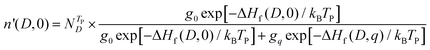 | (7) |
| |  | (8) |
where

is the total defect density. When the doped samples are quenched from
TP to room temperature, the carrier densities and Fermi energy can be obtained by solving
eqn (3)–(8) self-consistently.
We constructed chemical potential diagrams by considering the total energies of all competing phases, and set the mixing parameter α with the same value for every impurity phase. The input files are generated by using the vise code21 and executed with the Pydefect package.21 All competing phases are screened from the Materials Project Database (MPD).29 The chemical potentials are determined from the MPD when calculating the formation energy of each defect.21,30
The transport properties of the carriers are evaluated using the AMSET package,31 in which the carrier scattering rate and mobility can be obtained via the momentum relaxation time approximation by solving the Boltzmann transport equation.32
3. Results and discussion
3.1. Crystal and electronic structures
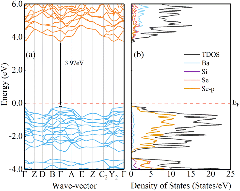
The crystal structure of Ba2SiSe4 is monoclinic, and it belongs to the P21/m space group. The optimized results are shown in Table S1 of the ESI.† Compared to the experimental values,33 the difference is less than 2.5%, suggesting our geometrical optimizations are credible. Based on the doubly screened hybrid functional and a fixed μ = 0.71 Bohr−1,34–36 the calculated band gap of Ba2SiSe4 is 3.51 eV, which is smaller than the reported value (3.96 eV).15,16 To reproduce the 3.96 eV band gap as reported earlier,15,16 we chose to increase the mixing parameter α in the HSE hybrid functional.37,38 When α is increased to 0.45, the calculated band gap for Ba2SiSe4 is 3.97 eV. The corresponding band structures and density of states (DOS) are shown in Fig. 1(a) and (b), respectively. The highly curved conduction band (valence band) indicates that the material has a low effective mass of electrons (holes). The effective mass of the hole for Ba2SiSe4 is only 0.21m0 along the Γ–Z direction. A smaller hole effective mass means a better hole mobility and p-type electrical conductivity.39 The DOS of Ba2SiSe4 show that the VBM is mainly from the Se-3p orbitals (Fig. 1(b)).
 |
| | Fig. 1 Band structures for Ba2SiSe4, calculated using the HSE, α = 0.45, are plotted in (a). The corresponding DOS are shown in (b). The Fermi energy is set to 0 eV. | |
3.2. The tendency of p-type electrical conductivity of Ba2SiSe4
To understand the doping tendency, the band arrangement, along with the ionization energies of the donor and acceptor, is investigated. The empirical guidelines show that it is easier to achieve n (p)-type doping in WGSs if the conduction band maximum (valence band maximum) is deeper (shallower) than −4.00 (−6.00) eV.40,41 The band arrangement of Ba2SiSe4 with other existing WGSs are shown in Fig. 2(a). Based on the vacuum energy levels, we calculated the positions of the VBM and CBM of Ba2SiSe4, and the corresponding results are −4.80 eV and −0.80 eV, respectively. The VBM of Ba2SiSe4 is significantly higher than those of common WGSs, which can be attributed to the dominance of the high Se-p orbitals (Fig. 1(b)). A higher VBM suggests p-type defects and electrical conductivity in Ba2SiSe4.
 |
| | Fig. 2 Electronic band alignment of Ba2SiSe4 with existing typical WGSs plotted in panel (a). The value for Ba2SiSe4 is calculated using the HSE, while the others are experimental values.40,47–52 The ionization energy difference of Ba2SiSe4 with existing WGSs is shown in panel (b). | |
Ionization energy has a significant impact on the defect properties of wide-gap semiconductors. A lower (higher) acceptor (donor) ionization energy is beneficial for increasing the number of hole carriers, thereby enhancing p-type conductivity.42 The ionization energy criterion, proposed by Gao et al., is expressed as:43
where
EAI (
EDI) represents the acceptor (donor) ionization energy. The ionization energies can be estimated using the hydrogen-like model:
44,45| |  | (10) |
Here,
m* (
m0) represents the effective mass of carriers (mass of the electron), and
εr is the relative dielectric constant. According to the ionization energy criterion, compounds with an ionization energy difference (Δ
E) of less than 0.15 eV can be identified as intrinsic p-type WGSs.
46 The ionization energy is calculated and tabulated in Table S2 of the ESI.
† Also, comparisons with other WGSs are shown in
Fig. 2(b). A smaller Δ
E (only 0.008 eV) suggests that Ba
2SiSe
4 can be doped to form p-type WGS.
43 Which defect is the shallow p-type defect, and how to realize the shallow p-type defect is an interesting issue.
3.3. Screening of p-type defects
To study the behavior of defects, the point defects with all unequal sites are considered (including vacancies, anti-sites, and interstitial sites). The screening of the defects is performed using the GGA method, and the corresponding results are shown in Fig. S1 of the ESI.† The defects, with lower formation energies (less than 3.0 eV), are recalculated with the HSE hybrid functional scheme (α = 0.45).
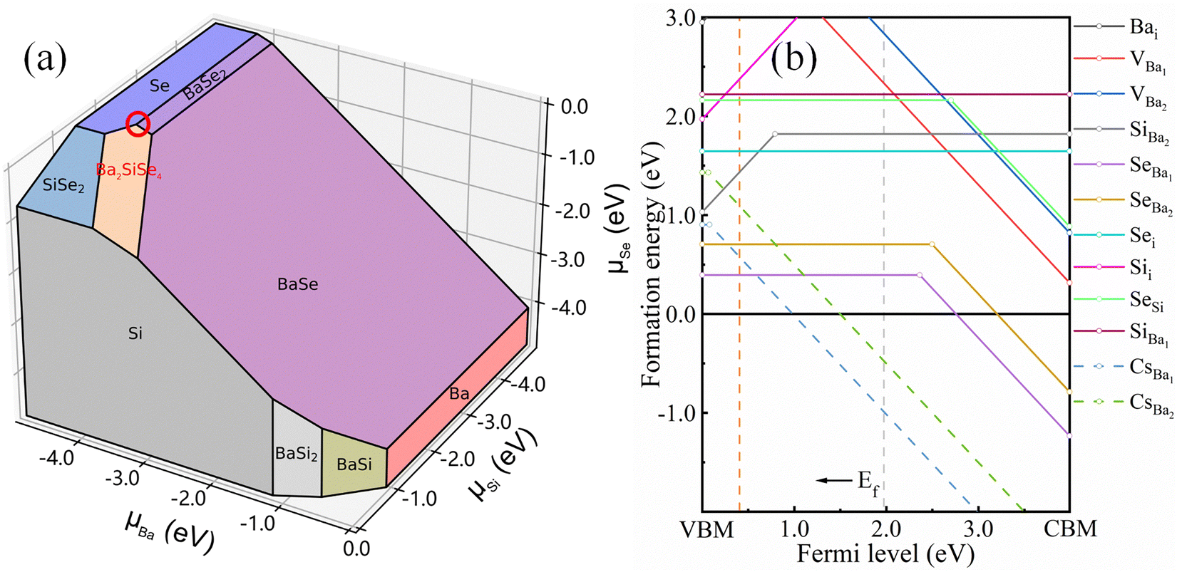
Considering all possible competing compounds, the chemical potential diagrams for Ba2SiSe4, with Ba, Se, and Se as variables, are plotted in Fig. 3(a). The stable region for single-phase Ba2SiSe4 is depicted by the saffron polygon, indicating that the Se-rich, Ba (Si)-poor condition is beneficial for forming Ba2SiSe4. Under the Se-rich, Ba (Si)-poor condition, the formation energies for all considered defects are calculated, and the corresponding results are plotted in Fig. 3(b).
 |
| | Fig. 3 Under thermodynamic conditions, the stable phase regions for Ba2SiSe4 in the Ba–Si–Se chemical-potential diagram are shown using the orange polygon (a). The defect formation energies, under Se-rich and Ba (Si)-poor conditions, are shown in panel (b). The chemical potential of Cs is determined from Cs2Se. The formation energy of externally doped Cs is also shown in panel (b). | |
Fig. 3(b) shows that two anti-site defects (SeBa1, SeBa2) possess low formation energies. This result is mainly due to the similar ionic radii of Se2− and Ba2+, which allows Se to occupy the octahedral sites through lattice relaxation. Conversely, the smaller radius of Si4+ induces significant localized lattice distortions, resulting in the higher formation energies for SiBa2 and Sii. Moreover, the transition energies ε(0/−) of SeBa1 and SeBa2 are higher than 2.50 eV above the VBM. These results indicate that SeBa1 and SeBa2 cannot be ionized and a high density of hole carriers is therefore impossible, which would seriously hinder p-type electrical conductivity. Hence, introducing an external impurity is necessary. We find that Cs substituting Ba1 (CsBa1) is a promising p-type defect. The formation energy for CsBa with the EF (dashed line) is shown in Fig. 3(b). Under the Se-rich, Ba (Si)-poor condition, the formation energy of neutral CsBa1 is 0.90 eV, indicating that the CsBa1 defects could be fabricated using the thermodynamic equilibrium fabrication scheme. The transition energy ε(0/−) for CsBa1 is only 0.081 eV above the VBM, suggesting that the defects CsBa1 could be ionized with a high density of holes in the samples.
3.4. The density of holes
Thermodynamic simulations of Cs doping in Ba2SiSe4 are conducted, taking into account the calculated defect formation and ionization energies, as well as the chemical potential stabilization region that was previously determined. Utilizing the electrically neutral condition, the defect density and hole density are calculated by self-consistently solving eqn (3)–(8). We employed a method of heating and quenching to room temperature (RT), which is a mature carrier density engineering method, to increase the hole density.27,28,53 Under thermodynamic equilibrium preparation conditions, Ba2SiSe4 is grown at high preparation temperatures (TP) to increase the hole density. At the same time, when Ba2SiSe4 is quenched to RT, the total number of defects does not change, and the hole density increases sharply due to redistributions in different charge states.10
Under the Se-rich, Ba (Si)-poor condition, the calculated Fermi energies, hole density, and major charge defect densities are plotted in Fig. 4, and the gray dashed line indicates the experimental preparation temperature (974.0 K) of Ba2SiSe4.33 The Ef decreases from 0.40 eV to 0.27 eV (point A, Fig. 4(a)) when the TP increases from 300.0 to 974.0 K. This finding suggests an increase in the hole density of Ba2SiSe4. As illustrated in Fig. 4(b), the hole density exhibits an increase from 8.31 × 1011 cm−3 to 4.04 × 1017 cm−3 due to quenching from 974.0 K to 300.0 K (orange line). This phenomenon is primarily attributed to the high solubility of CsBa1 at high TP. At the same time, the higher formation energy of the hole killers SiBa2 and Sii makes thesehole quencher defects play a minor role compared to that of CsBa1 under the same growth conditions. As illustrated in Fig. 4(c), the density of CsBa1 can reach 1.06 × 1018 cm−3 (974.0 K). This result is attributed to the lower defect formation energy and transition energy ε(0/−) of CsBa1. Compared to the traditional p-type WGSs, such as ZnGa2O4 (1.60 × 1015 cm−3)54 and CuAlO2 (1.3 × 1017 cm−3),55 Ba2SiSe4 possesses competitive p-type electrical conductivity. The detailed discussion of carrier densities is tabulated in Table S4 of the ESI.† To achieve a higher density of holes in Cs-doped Ba2SiSe4, it is necessary to consider non-equilibrium preparation methods,56 such as the molecular beam epitaxy scheme.9
 |
| | Fig. 4 The calculated Fermi energy, hole density, and defect density in Cs-doped Ba2SiSe4 are shown in panels (a)–(c). PT (RT) represents the results calculated at preparation temperatures (after quenching to room temperature). | |
3.5. Hole mobility and p-type electrical conductivity
In order to further characterize the p-type electrical conductivity of Ba2SiSe4, the charge transport behaviors are analyzed using the AMSET package.31 Hole mobility with the hole density at room temperature is presented in Fig. 5(a), which shows that at lower carrier densities (not exceeding 1018 cm−3), the maximum mobility of holes is approximately 5.20 cm2 V−1 s−1. When the hole density reaches 2.5 × 1017 cm−3, the hole mobility for conventional p-type WGSs SnO is only 2.4 cm2 V−1 s−1,57 while the hole mobility of Ba2SiSe4 could reach 5.1 cm2 V−1 s−1. The effects of scattering mechanisms on the hole mobility for Ba2SiSe4 at a carrier density of 4.04 × 1017 cm−3 are shown in Fig. 5(b). The polar optical phonon scattering (POP) emerges as the predominant limiting factor at higher temperatures. At the same time, the mobility of Ba2SiSe4 declines with increasing temperature, which is similar to most semiconductors.58
 |
| | Fig. 5 The calculated hole mobility of Ba2SiSe4 as a function of carrier density at room temperature is shown in panel (a). The effect of the scattering mechanism on the mobility at specific hole densities is plotted in panel (b). ADP is acoustic deformation potential scattering, IMP is ionized impurity scattering, and POP is polar optical phonon scattering. The p-type electrical conductivity of Ba2SiSe4 with temperature at different hole densities is shown in panel (c). | |
The p-type electrical conductivity as a function of temperature at different hole carrier densities is shown in Fig. 5(c). In general, the electrical conductivity of a material decreases with increasing temperature. The main reason is that the vibration of the lattice structure increases with temperature, which leads to an increase in the probability of carrier scattering.59 This inhibits the movement of free carriers, thereby reducing the conductivity of Ba2SiSe4. After quenching from 974.0 K to RT, hole density (4.04 × 1017 cm−3) and p-type electrical conductivity (32.3 S m−1) (based on the thermodynamic impurity simulations) can be obtained in Ba2SiSe4. Under similar hole density conditions, the p-type electrical conductivity of Ba2SiSe4 is significantly higher than that of CuGaO2 (2.0 S m−1)60 and Cu2O (19.0 S m−1).61
4. Conclusion
In this work, the p-type electrical conductivity for Ba2SiSe4 is studied. Our analysis reveals that Ba2SiSe4 exhibits superior potential for p-type conductivity, as evidenced by its band alignment, ionization energy, and electronic band structure characteristics. Under the Se-rich, Ba (Si)-poor condition, the formation energy of CsBa1 is 0.90 eV with high defect solubility. Based on the thermodynamic equilibrium simulation, Ba2SiSe4 was quenched to room temperature from the preparation temperature, and the hole density reached 4.04 × 1017 cm−3. The hole mobility of Ba2SiSe4 at this carrier density is 5.2 cm2 V−1 s−1, and the p-type electrical conductivity is 32.3 S m−1, which exceeds the traditional p-type WGSs. The simulation results indicated that Cs-doped Ba2SiSe4 may be a new p-type WGS with higher hole mobility and p-type electrical conductivity. The p-type electrical conductivity could exceed 104 S m−1 using the non-equilibrium preparation method. This work stimulates the development of p-type WGSs and provides a fundamental guideline for fabricating high-efficiency optoelectronic devices.
Author contributions
Yuhang Deng: investigation, visualization, validation, conceptualization, methodology formal analysis, and writing – original draft. Qiao Wei: visualization, validation, investigation, and data curation. Liu Yang: writing – review and editing, visualization, methodology, and funding acquisition. Shuaiwei Fan: supervision, software, resources, project administration, investigation, conceptualization, data curation, funding acquisition, and writing – review and editing.
Conflicts of interest
There are no conflicts to declare.
Data availability
The data supporting this article have been included as part of the ESI.†
Acknowledgements
This work is supported by the Natural Science Foundation of Hubei Province (No. 2025AFB092) and Natural Science and Technology Foundation of Yichang (No. A22-3-006).
References
- S. C. Liu, Y. S. Yang, Z. B. Li, D. J. Xue and J. S. Hu, Mater. Chem. Front., 2020, 4, 775–787 RSC.
- V. Q. Le, T. H. Do, J. R. D. Retamal, P. Shao, Y. H. Lai, W. Wu, J. H. He, Y. L. Chueh and Y. H. Chu, Nano Energy, 2019, 56, 322–329 CrossRef CAS.
- Z. Wang, Y. J. Gu, X. M. Li, Y. Liu, F. H. Liu and W. P. Wu, Adv. Opt. Mater., 2023, 11, 2300970 CrossRef CAS.
- Z. R. Wang and G. Z. Shen, Mater. Chem. Front., 2023, 7, 1496–1519 RSC.
- I. Hamberg and C. G. Granqvist, J. Appl. Phys., 1986, 60, R123–R160 CrossRef CAS.
- D. Y. Zhang, W. H. Yu, L. Zhang and X. Y. Hao, Materials, 2023, 16, 5537 CrossRef.
- A. N. Fioretti and M. Morales-Masis, J. Photonics Energy, 2020, 10, 042002 Search PubMed.
- V. Ha, F. Ricci, G. Rignanese and G. Hautier, J. Mater. Chem. C, 2017, 5, 5772–5779 RSC.
- S. W. Fan, Y. Chen and L. Yang, J. Phys. Chem. C, 2022, 126, 19446–19454 CrossRef.
- Y. Chen, S. W. Fan and G. Y. Gao, Mater. Sci. Semicond. Process., 2022, 151, 107024 CrossRef.
- Y. Chen, L. Yang, Z. L. Wang and S. W. Fan, Solid State Commun., 2022, 359, 115013 CrossRef.
- S. Hadke, M. L. Huang, C. Chen, Y. F. Tay, S. Y. Chen, J. Tang and L. Wong, Chem. Rev., 2022, 122, 10170–10265 CrossRef PubMed.
- X. T. Zhang, C. Q. Lin, X. Y. Guo, Y. Xue, X. Q. Liang, W. Z. Zhou, C. Persson and D. Huang, J. Phys. Chem. Solids, 2024, 190, 112002 CrossRef.
- S. X. Kang, J. Y. Wang, L. Yang and S. W. Fan, Phys. Scr., 2024, 99, 035923 CrossRef.
- J. Y. Wang and S. W. Fan, ACS Appl. Opt. Mater., 2024, 2, 1999–2010 CrossRef.
- R. Kormath Madam Raghupathy, H. Wiebeler, T. D. Kühne, C. Felser and H. Mirhosseini, Chem. Mater., 2018, 30, 6794–6800 CrossRef.
- J. Heyd, G. E. Scuseria and M. Ernzerhof, J. Chem. Phys., 2003, 118, 8207–8215 CrossRef.
- A. V. Krukau, O. A. Vydrov, A. F. Izmaylov and G. E. Scuseria, J. Chem. Phys., 2006, 125, 224106 CrossRef PubMed.
- W. Kohn and P. Hohenberg, Phys. Rev., 1964, 136, B864–B871 CrossRef.
- G. Kresse and J. Furthmüller, Comput. Mater. Sci., 1996, 6, 15–50 CrossRef CAS.
- Y. Kumagai, N. Tsunoda, A. Takahashi and F. Oba, Phys. Rev. Mater., 2021, 5, 123803 CrossRef CAS.
- Y. Kumagai, Phys. Rev. Appl., 2023, 19, 034063 CrossRef CAS.
- J. Neugebauer, C. G. Van de Walle and C. Freysoldt, Phys. Rev. Lett., 2009, 102, 016402 CrossRef PubMed.
- F. Oba and Y. Kumagai, Phys. Rev. B: Condens. Matter Mater. Phys., 2014, 89, 195205 CrossRef.
- Y. Kumagai, F. Oba and T. Gake, Phys. Rev. Mater., 2019, 3, 044603 CrossRef.
- S. W. Fan, J. Y. Chang, L. Yang and G. W. Hu, J. Mater. Chem. C, 2025, 13, 7150–7158 RSC.
- S. H. Wei, T. A. Gessert, K. K. Chin and J. Ma, Phys. Rev. B: Condens. Matter Mater. Phys., 2011, 83, 245207 CrossRef.
- J. Park, J. Kang, W. Metzger, T. Barnes, S. H. Wei and J. H. Yang, Phys. Rev. B: Condens. Matter Mater. Phys., 2014, 90, 245202 CrossRef.
- A. Jain, S. P. Ong, G. Hautier, W. Chen, W. D. Richards, S. Dacek, S. Cholia, D. Gunter, D. Skinner, G. Ceder and K. A. Persson, APL Mater., 2013, 1, 011002 CrossRef.
- A. Wang, R. Kingsbury, M. Mcdermott, M. Horton, A. Jain, S. P. Ong, S. Dwaraknath and K. A. Persson, Sci. Rep., 2021, 11, 15496 CrossRef CAS.
- A. M. Ganose, J. Park, A. Faghaninia, R. Woods-Robinson, K. A. Persson and A. Jain, Nat. Commun., 2021, 12, 2222 CrossRef CAS PubMed.
- S. Hachmioune, A. M. Ganose, M. B. Sullivan and D. O. Scanlon, Chem. Mater., 2024, 36, 6062–6073 CrossRef CAS.
- C. Brinkmann, B. Eisenmann and H. Schäfer, Z. Anorg. Allg. Chem., 1985, 524, 83–89 CrossRef CAS.
- Z. H. Cui, Y. C. Wang, M. Y. Zhang, X. Xu and H. Jiang, J. Phys. Chem. Lett., 2018, 9, 2338–2345 CrossRef CAS.
- J. Yang, S. Falletta and A. Pasquarello, Npj Comp. Mater., 2023, 9, 108 CrossRef.
- I. B. Garba, L. Trombini, C. Katan, J. Even, M. Zacharias, M. Kepenekian and G. Volonakis, Acs Mater. Lett., 2025, 7, 1922–1929 CrossRef CAS.
- M. Lorke, B. Aradi, T. Frauenheim and P. Deák, Phys. Rev. B, 2019, 99, 085206 CrossRef.
- S. X. Kang, S. W. Fan, L. Yang and G. W. Hu, Appl. Mater. Today, 2025, 42, 102572 CrossRef.
- M. Zhong, W. Zeng, F. S. Liu, D. H. Fan, B. Tang and Q. J. Liu, Mater. Today Phys., 2022, 22, 100583 CrossRef CAS.
- Z. W. Xiao, C. Qiu, S. H. Wei and H. Hosono, Chin. Phys. Lett., 2025, 42, 016103 CrossRef CAS.
- M. T. Greiner and Z. Lu, NPG Asia Mater., 2013, 5, e55 CrossRef CAS.
- S. J. Clark and J. Robertson, Phys. Rev. B: Condens. Matter Mater. Phys., 2011, 83, 075205 CrossRef.
- J. Gao, W. Zeng, R. B. Luo, Z. T. Liu and Q. J. Liu, Cryst. Growth Des., 2024, 24, 3777–3785 CrossRef CAS.
- D. M. Eagles, J. Phys. Chem. Solids, 1960, 16, 76–83 CrossRef CAS.
- C. Tablero, Comput. Mater. Sci., 2010, 49, 368–371 CrossRef CAS.
- R. Y. Cao, H. X. Deng and J. W. Luo, ACS Appl. Mater. Interfaces, 2019, 11, 24837–24849 CrossRef CAS PubMed.
- M. Liao, S. Takemoto, Z. W. Xiao, Y. Toda, T. Tada, S. Ueda, T. Kamiya and H. Hosono, J. Appl. Phys., 2016, 119, 165701 CrossRef.
- J. Pellicer-Porres, A. Segura, A. S. Gilliland, A. Muñoz, P. Rodríguez-Hernández, D. Kim, M. S. Lee and T. Y. Kim, Appl. Phys. Lett., 2006, 88, 181904 CrossRef.
- R. Brahimi, B. Bellal, Y. Bessekhouad, A. Bouguelia and M. Trari, J. Cryst. Growth, 2008, 310, 4325–4329 CrossRef CAS.
- M. N. Islam and M. O. Hakim, J. Mater. Sci. Lett., 1986, 5, 63–65 CrossRef CAS.
- H. Köstlin, R. Jost and W. Lems, Phys. Status Solidi A, 1975, 29, 87–93 CrossRef.
- R. Summitt, J. A. Marley and N. F. Borrelli, J. Phys. Chem. Solids, 1964, 25, 1465–1469 CrossRef CAS.
- Y. Chen, S. W. Fan and P. Xu, Appl. Phys. Lett., 2022, 121, 252102 CrossRef CAS.
- M. Minohara, Y. Dobashi, N. Kikuchi, A. Samizo, K. Tsukuda, K. Nishio, K. Mibu, H. Kumigashira, I. Hase, Y. Yoshida and Y. Aiura, Inorg. Chem., 2021, 60, 8035–8041 CrossRef CAS PubMed.
- H. Kawazoe, M. Yasukawa, H. Hyodo, M. Kurita, H. Yanagi and H. Hosono, Nature, 1997, 389, 939–942 CrossRef CAS.
- J. B. Xia, J. Semicond., 2021, 42, 060402 CrossRef.
- Y. Ogo, H. Hiramatsu, K. Nomura, H. Yanagi, T. Kamiya, M. Hirano and H. Hosono, Appl. Phys. Lett., 2008, 93, 032113 CrossRef.
- J. Willis, R. Claes, Q. Zhou, M. Giantomassi, G. Rignanese, G. Hautier and D. O. Scanlon, Chem. Mater., 2023, 35, 8995–9006 CrossRef CAS PubMed.
- K. Li, J. Willis, S. R. Kavanagh and D. O. Scanlon, Chem. Mater., 2024, 36, 2907–2916 CrossRef CAS PubMed.
- K. H. L. Zhang, K. Xi, M. G. Blamire and R. G. Egdell, J. Phys.: Condens. Matter, 2016, 28, 383002 CrossRef.
- R. B. Xue, G. Gao, L. Yang, L. G. Xu, Y. M. Zhang and J. Q. Zhu, J. Mater. Chem. C, 2023, 11, 13681–13690 RSC.
|
| This journal is © The Royal Society of Chemistry 2025 |
Click here to see how this site uses Cookies. View our privacy policy here. 
 a,
Qiao
Wei
a,
Qiao
Wei


 represents the effective mass of the electron (hole). h is the Planck's constant. The charge-neutral condition is necessary when introducing charged defects into the semiconductors:27,28

 is the total defect density. When the doped samples are quenched from TP to room temperature, the carrier densities and Fermi energy can be obtained by solving eqn (3)–(8) self-consistently.