
 Open Access Article
 This Open Access Article is licensed under a Creative Commons Attribution-Non Commercial 3.0 Unported Licence
Vertical p–i–p perovskite photoconductors combining intrinsic and doped organic transport layers†
Lucía Martínez-Goyeneche,
Serhii Derenko,
Alejandra Silva-Mayo,
Daniel Tordera and
Michele Sessolo*
and
Michele Sessolo*
Instituto de Ciencia Molecular, Universidad de Valencia, C/Catedrático J. Beltrán 2, 46980 Paterna, Spain. E-mail: michele.sessolo@uv.es
First published on 10th July 2025
Abstract
Photoconductors are a class of photodetectors that can exhibit photoconductive gain, a key advantage for achieving high sensitivity. While most reported devices rely on lateral architectures, here we present fully vacuum-deposited vertical p–i–p perovskite photoconductors based on methylammonium lead iodide (MAPI). The influence of hole transport layers (HTLs), both intrinsic and doped, was systematically investigated. Devices incorporating intrinsic HTLs show significantly reduced dark currents, particularly when the intrinsic layer is sufficiently thick. When intrinsic and doped HTLs are combined, the devices benefit from both suppressed dark current and enhanced charge extraction, leading to superior performance. Optimized structures achieve quantum efficiency >3000% and high on/off ratio, demonstrating the potential of this vertical architecture for highly sensitive optoelectronic applications.
Introduction
Semiconducting metal halide perovskites (herein simply perovskites) have attracted significant attention in optoelectronics due to their suitable properties: high optical absorption coefficient,1 tuneable and direct bandgap,2–5 high defect tolerance,6,7 low dark current8–10 and high charge mobility.11–13 For this reason, perovskites have been applied to a variety of devices such as solar cells,14–18 photodetectors,19–22 lasers,23,24 and light-emitting diodes.25–27 Photodetectors are optoelectronic devices that transduce light into electrical signals, in the form of either current or voltage. They can be broadly classified as photodiodes, photoconductors, and photomultiplication detectors. Photodiodes are widely used vertical devices, as they are fast and reliable, with external quantum efficiency (EQE) maximum at unity, as each absorbed photon can only trigger one charge carrier.19,28–31 On the other hand, photoconductors (PCs) are typically lateral devices with symmetrical electrodes, mostly reported using perovskite single crystals.32–34 PCs can achieve EQE values above unity, as one incident photon can lead to a charge carrier circulating several times within the device, a phenomena referred to as photoconductive gain.35–37 This gain comes from defects/trap states that capture the minority charge carriers (either holes or electrons), allowing the majority charge carriers to flow multiple times through the external circuit.38,39 As mentioned, most of the reported PCs are lateral devices, with only very few works describing vertical structures. For instance, Zhang et al. designed a photoconductive device with a photodiode structure comprising an electron transport layer of C60 (fullerene) doped with 2,3,5,6-tetrafluoro-7,7,8,8-tetracyanoquinodimethane (F4-TCNQ), in which the dopant provided deep trap states to capture the photogenerated electrons from the perovskite (electron trapping). The hole injection barrier was thin enough to allow holes to tunnel through, resulting in hole injection and gain.40 While representing a neat example, the device is a photomultiplication-type detector rather than a photoconductor, as it rectifies as a diode in the dark and shows gain under illumination. Zhao et al. demonstrated vertical perovskite PCs with the structure ITO/C60/MAPI/C60/Ag, where the incorporation of the charge transport layer, C60, improved the crystal quality of the solution-processed (spin-coated) perovskite, and enhanced the EQE and the photocurrent of the methylammonium lead iodide (MAPI) photodetector.41 The characterization of the device was however limited to the EQE, with no description of the photo- and dark currents of the device. Hence, to our knowledge, there has been no thorough study on the effect of the transport layers on the performance of vertical perovskite PCs, and we haven’t found reports on vapour-deposited PCs employing multilayer transport layers. Vapour or vacuum deposition of perovskite devices offers several advantages. Importantly, physical vapour deposition techniques are already well established in industry for large-area processing. Being solvent-free, these methods eliminate the need for thermal post-processing, enabling integration with sensitive substrates such as plastic foils. Moreover, vapour deposition allows the fabrication of multilayer devices with arbitrary thicknesses—capabilities that are difficult to achieve with solution-based processing.42–44In this work, we fabricate fully vacuum-deposited perovskite PCs, where the perovskite layer is sandwiched between two organic hole transport layers (HTLs) in a vertical p–i–p configuration. We study the influence of the incorporation of HTLs (both intrinsic and doped) on the performance of the devices, as well as the effect of the thickness of the transport layers and the dopant concentration. We show that intrinsic HTLs are essential to reduce dark current in vertical PCs. Moreover, when combining intrinsic and doped HTLs, the devices benefit from both layers, with a reduction of the dark current (intrinsic HTL) and an improved charge extraction/transport (doped HTL). EQE >3000% and high on/off ratio were obtained for devices with high dopant concentrations and thick intrinsic hole transport layers.
Results and discussion
Vertical perovskite PCs in a p–i–p configuration (p-type organic/intrinsic perovskite/p-type organic) were fabricated with the following stack: glass/ITO/HTL/MAPI/HTL/Ag, where ITO is indium tin oxide. The HTLs were systematically varied on either side of the active layer and on both sides. The organic semiconductor used as the HTL is N4,N4,N4′′,N4′′-tetra([1,1′-biphenyl]-4-yl)-[1,1′:4′,1′′-terphenyl]-4,4′-diamine (TaTm). When indicated, TaTm was doped with 2,2′-(perfluoronaphthalene-2,6-diylidene) dimalononitrile (F6-TCNNQ). We also explore multilayers of TaTm and TaTm:F6-TCNNQ. All layers were deposited by thermal vacuum deposition. Details on the processing can be found in the methods section.We initially fabricated simple PCs by depositing 500 nm thick MAPI films directly on an ITO-coated glass, and coating the perovskite with a 100 nm thick silver electrode (Fig. 1a). Dark and photocurrent density versus voltage (J–V) characteristics of the PCs were measured only in the reverse bias quadrant, from −2 to 0 V, which is relevant for applications. In this way we can neglect current hysteresis between the forward and reverse voltage scans, resulting from the coexistence of electronic and ionic transport within the perovskite itself,45 phenomena that are not within the motivation of this work. The reference ITO/MAPI/Ag device shows an ohmic behaviour both in the dark and under illumination (see linear J–V scan in Fig. S1a, ESI†). The dark current density (Jdark) is, however, very high (nearly 800 mA cm−2 at −2 V), and the current density under illumination (Jph) is only slightly higher, with a rather voltage-independent on/off ratio Jph/Jdark between 1.3 and 1.4. This device configuration might suffer from two different effects: (i) the MAPI film is evaporated directly onto a metal oxide (ITO), which is known to retard and alter the perovskite formation from the vapour phase,46,47 and (ii) the Ag electrode is directly evaporated onto the perovskite, inducing damage and/or chemical reactions at the MAPI/Ag interface.48
 | ||
| Fig. 1 Electrical characterization of vertical photoconductors with (a) electrodes only, (b) intrinsic HTLs, (c) doped HTLs and (d) a combination of intrinsic and doped HTLs. On the left axes, J–V characteristics in the dark (blue line) and under 100 mW cm−2 illumination (orange line). On the right, the corresponding calculated on/off ratio between Jph and Jd (red line). | ||
Inspired by our previous work on vacuum-deposited perovskite solar cells and photodiodes employing organic transport layers, we studied the influence of using intrinsic and doped organic semiconductors, as well as their combinations, at the interface between the perovskite and the electrodes.49,50 Intrinsic TaTm films are typically thin (10 nm) in view of their moderate mobility, while doped layers of the type TaTm:F6-TCNNQ (10 wt% doping) can be used thicker (40 nm) as they are more conductive.
When an intrinsic, 10 nm thick, TaTm layer is introduced between the electrodes and the perovskite, the dark current (Fig. 1b and Fig. S1b, ESI†) is slightly reduced, while the photocurrent increases, leading to a larger Jph/Jd ratio >3. This might result from reduced shunts, alleviating detrimental effects at the interfaces as discussed above. When thicker, doped TaTm:F6-TCNNQ layers (Fig. 1c) are used, we observed a noticeable reduction of the dark current (more than 3 orders of magnitude), approximately 0.1 mA cm−2 at −1 V, and increasing to approximately 2 mA cm−2 at −2 V. Compared to the device with TaTm only, the photocurrent is also slightly reduced, most likely due to parasitic absorption. However, the net result is a maximum Jph/Jd ratio of 850 at −1.5 V. At higher bias, the on/off ratio diminishes due to the increasing Jd, while at lower bias it is limited by the JPh. Finally, we evaluated the incorporation of both intrinsic and doped charge transport layers, as commonly used on efficient perovskite solar cells.49,51 When the combination of intrinsic and doped layers is symmetrically placed at the electrode interfaces (Fig. 1d), the photocurrent is essentially unaltered (compared to the PCs with doped HTLs), but a further reduction of the dark current is observed, in the range from 0 to −1.5 V. As a consequence, a maximum Jph/Jd ratio exceeding 1600 is obtained between −0.5 and −0.75 V, monotonically reducing (due to increasing Jd) to >250 at 2 V. In this case, the doped layer is used at the interface with the electrodes, to match the work function ensuring ohmic charge injection/extraction, while the intrinsic HTLs are used at the interface with the perovskite, to reduce charge recombination and induce carrier-type selectivity. Both concepts, arising from photovoltaics and light-emitting diodes, seem to be also beneficial in these vertical PCs.
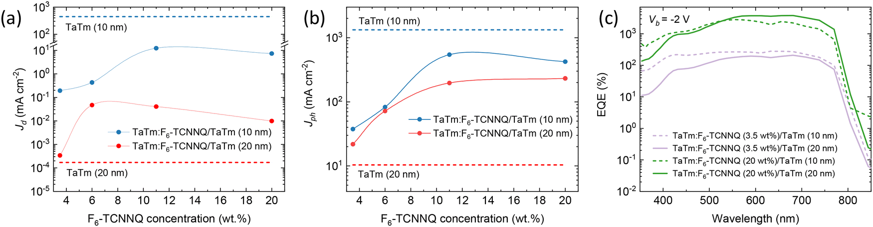
Subsequently, we investigated the influence of the intrinsic HTL thickness and dopant concentration on both the dark current and photocurrent in the vertical PCs. The J–V curves for devices with the structure ITO/TaTm/MAPI/TaTm/Ag and with two thicknesses of TaTm (10 nm and 20 nm), are shown in Fig. 2a. We observed a striking reduction of Jd when increasing the thickness of TaTm to 20 nm, to values below 10−4 mA cm−2, which fall within the noise region of our measurement setup. To our knowledge, such low dark current density has not yet been reported for vertical perovskite photoconductors.41,52 This is likely a consequence of the increased injection/extraction barrier at the electrode interface, and partially of the thicker HTLs, with a lower mobility compared to the perovskite. Jph also diminishes with thicker TaTm, but in general the on/off ratio is much higher compared to the same device with 10 nm thick TaTm (albeit not quantified in this case, in view of the noise in Jd). We then introduced the doped HTLs at the electrode interfaces, and systematically varied the doping concentration during co-deposition of TaTm and F6-TCNNQ (from 3.5 to 20 wt%). For devices with 10 nm thick TaTm, increasing the dopant concentration (Fig. 2b) leads to an increased Jd in the high bias region (below −1 V), approximately varying from 0.2 to 10 mA cm−2 at −2 V. The photocurrent is found to scale with the doping concentration, reaching Jph > 350 mA cm−2 (between −1 and −2 V) for the samples with doping concentration of 11 and 20 wt%. More interesting is the profile of the on/off ratio, whose maximum shifts towards lower applied bias with increasing doping. At low voltage, the on/off ratio is higher for the PCs including doped layers at high F6-TCNNQ concentration, with maxima between approximately 5 × 10³ and 104 for the 20 and 11 wt% dopant, respectively. However, due to the rapid increase in Jd with applied bias in these devices, the on/off ratio monotonically decreases as the voltage becomes more negative, reaching values between 40 and 60 at −2 V. At this same bias, devices with lower dopant concentrations exhibit a slightly higher on/off ratio, around 200. For these samples, the on/off ratio also increases as the voltage becomes more positive, peaking at approximately 800 and 350 for dopant concentrations of 6 wt% and 3.5 wt%, respectively.
 | ||
| Fig. 2 (a) J–V curves under illumination (dashed) and in the dark (solid) of vertical PCs employing solely intrinsic HTLs (schematic of the device structure above the graph). J–V curves under illumination (dash) and in the dark (line) of vertical PCs using a combination of doped transport layers with increasing doping levels and either a (b) 10 nm or (d) 20 nm thick intrinsic HTL (schematic of the device structure on the top left). On the bottom, the profile of the on/off ratio (c) and (e) calculated from the J–V curves in (b) and (d), respectively (schematic of the device structure to the left of graph (b)). | ||
When the thickness of the intrinsic TaTm is increased to 20 nm, Jd is generally reduced (Fig. 2d), as observed for the simpler devices in Fig. 2a. Jd remains below 10−3![[thin space (1/6-em)]](https://www.rsc.org/images/entities/char_2009.gif) mA cm−2 at reverse bias up to −2 V for the 3.5 and 6 wt% samples. As the dopant concentration increases, Jd also increases substantially, particularly evident at 11 and 20 wt%, where it reaches a maximum of up to 10−1mA cm−2, indicating enhanced conductivity with doping.
mA cm−2 at reverse bias up to −2 V for the 3.5 and 6 wt% samples. As the dopant concentration increases, Jd also increases substantially, particularly evident at 11 and 20 wt%, where it reaches a maximum of up to 10−1mA cm−2, indicating enhanced conductivity with doping.
Under illumination, all devices show a significant increase in current density across the entire bias range. The current density enhancement is particularly pronounced for the 11 and 20 wt% samples, with Jph exceeding 102mA cm−2 near −2 V. Lower dopant concentrations (3.5 and 6 wt%) still show clear photoresponse, although with more modest photocurrent values. As compared to the devices with thinner intrinsic TaTm, Jd is lower while Jph varies only modestly. As a consequence, the on/off ratios (Fig. 2e) are also enhanced. The device with 6 wt% doping concentration shows a very high but not representative on/off ratio at low bias, resulting in the combination of very low Jd and high Jph. In a more realistic working regime (<−0.5 V), however, the on/off ratio diminishes rapidly, reaching a minimum of >103 at −2 V. For the PCs with a lower F6-TCNNQ concentration, the on/off ratio shows less bias-dependency and is very high, up to 105, a consequence of the very low Jd. For higher doping concentrations, the maxima of the on/off ratio are located at approximately −1.5 V, and increase from 7.5 × 10³ to 5.5 × 10⁴ for 11 and 20 wt% dopants, respectively. Overall, these PCs, which incorporate an intrinsic 20 nm TaTm layer combined with highly doped TaTm, exhibit the best performance among all devices presented thus far. They deliver a simultaneously high photocurrent and a very large on/off ratio, highlighting their potential for efficient light detection.
We also quantified the photoresponse of selected vertical PCs to different light intensities. Here the photocurrent was recorded from 100 mW cm−2 down to 10−5 mW cm−2, by using a solar simulator and neutral density filters. The linear dynamic range (LDR), defined as the range over which Jph maintains a linear relationship with incident light intensity, was estimated using the expression LDR = 20 × log(Pmax/Pmin), where Pmax and Pmin represent the maximum and minimum light intensities within the linear response regime of the detector.20,53,54 The linear dynamic range was calculated for the photoconductors with the stack ITO/doped-TaTm/TaTm/MAPI/TaTm/doped-TaTm/Ag, for the two thicknesses of TaTm (10 and 20 nm) and for the two extreme dopant concentrations (3.5 and 20 wt%, respectively). These devices show similar LDR values (Fig. S2, ESI†), approximately 90 dB and 80 dB for photoconductors with 3.5 wt% and 22 wt%, respectively.
Fig. 3a summarizes Jd values measured at −2 V for all devices reported so far. Devices incorporating a sufficiently thick HTL, as indicated by the red dashed line, exhibit strongly suppressed Jd on the order of 10−4 mA cm−2. In contrast, devices combining a 20 nm intrinsic TaTm layer and additional 40 nm thick doped TaTm:F6-TCNNQ film, show a non-linear increase in Jd with increasing dopant concentration (red dots), reaching 2.8 × 10⁻² mA cm−2 for a 20 wt% dopant concentration. On the other hand, when the intrinsic TaTm thickness is reduced to just 10 nm (blue dashed line), the dark current increases dramatically to approximately 10−3 mA cm−2, highlighting the importance of sufficient (intrinsic) layer thickness for suppressing leakage currents. Devices incorporating both intrinsic and doped HTLs within this thinner configuration (blue dots) show comparatively lower Jd, indicating that even a modest intrinsic layer can provide a beneficial barrier when paired with a doped transport layer.
 | ||
| Fig. 3 Summary of the detector signals at a −2 V applied bias for the series of devices discussed in this work, with only an intrinsic HTL (dash lines) and a combination of intrinsic and doped-HTL (dots, the lines are a guide to the eye) at different dopant concentrations: (a) dark current and (b) photocurrent. (c) EQE spectra of selected vertical photoconductors, also measured at an applied bias of −2 V. | ||
Fig. 3b illustrates the corresponding Jph for all PCs. When the intrinsic TaTm layer is 20 nm thick, the combination of intrinsic and doped HTLs results in improved photocurrent, due to the increased electrical conductivity of the doped layer that results in a more efficient charge injection/transport, similar to what was previously reported for perovskite solar cells.55 However, this trend does not persist, and at the highest dopant concentration (20 wt%), the photocurrent begins to decline slightly compared to the 10 wt% case, likely due to the high absorbance of the doped-HTL, which introduces parasitic optical absorption. Therefore, there is a trade-off between improved charge extraction and parasitic absorption.
In summary, devices that combine intrinsic and doped HTLs benefit from both a low dark current thanks to the intrinsic layer, and a higher photocurrent due to the improved conductivity of the doped layer. Hence, we selected these PCs to estimate their spectral response. Fig. 3c shows the external quantum efficiency (EQE) of the photoconductors with ITO/doped-TaTm/TaTm/MAPI/TaTm/doped-TaTm/Ag, for the two thicknesses of TaTm (10 and 20 nm) and for the two extreme dopant concentrations (3.5 and 20 wt%, respectively). All devices exhibit EQEs exceeding unity, indicative of photoconductive gain. As schematically shown in Fig. S3 (ESI†), the gain in our devices originates from the unipolar nature of their structure. In the dark, only holes can be injected at moderate bias, as the energy barrier for electron injection from Ag into the LUMO of TaTm is too high. Under illumination, the perovskite becomes more conductive due to the generation of free carriers. However, the large energy offset between the perovskite conduction band and the LUMO of TaTm confines electrons within the perovskite. Holes, on the other hand, remain mobile and can circulate multiple times through the external circuit before recombining with the trapped electrons, resulting in EQE values exceeding unity.39 Devices with a thinner intrinsic TaTm layer (10 nm, dashed line) show higher EQE values in the UV-blue region of the spectrum (350–500 nm) compared to those with 20 nm of TaTm. This enhancement is attributed to reduced optical absorption in the thinner hole transport layer, allowing more light to reach the active perovskite layer. Furthermore, increasing the dopant concentration from 3.5 wt% to 20 wt% leads to a nearly two orders of magnitude increase in EQE, reaching values as high as 3800% at 680 nm. This trend is consistent with the previously observed photocurrent enhancement and reflects the improved charge transport and collection enabled by higher conductivity in the doped HTL. Finally, the specific detectivity (D*) was estimated assuming that shot-noise is the predominant source of the noise in the device (Fig. S4, ESI†).56–61 Devices with higher dark current (those with 10 nm of the intrinsic TaTm layer, dashed line), show lower D*, as expected. The maximum specific detectivity is 4 × 10¹³ Jones at −2 V for the devices with the combination of intrinsic (20 nm) and doped HTL (40 nm, 20% wt), which is in line with similar vertical perovskite photoconductors reported so far.41 However, this D* estimate is likely a rough overestimation as it does not account for other noise sources.62
Conclusions
We demonstrated fully vacuum-deposited p–i–p vertical photoconductors incorporating a methylammonium lead iodide (MAPI) perovskite active layer sandwiched between organic hole transport layers (HTLs). The role of the HTLs in determining device performance was systematically investigated by employing intrinsic TaTm, F6-TCNNQ-doped TaTm, and combinations of both. We further evaluated the influence of intrinsic HTL thickness and dopant concentration. The inclusion of intrinsic HTLs was found to be critical for suppressing the dark current, particularly when the TaTm thickness reached 20 nm, yielding values below 10−4mA cm−2. Devices combining intrinsic and doped HTLs benefitted from both low dark currents, enabled by the intrinsic layer, and relatively high photocurrents due to the enhanced conductivity of the doped HTL. Notably, photoconductors featuring thick intrinsic layers and high dopant concentrations achieved high performance, with external quantum efficiency (EQE) up to 3800% and on/off ratio >50000 at −2 V, highlighting the potential of this architecture for sensitive light detection applications.
Materials and methods
Materials
N4,N4,N4′,N4′-Tetra([1,1′-biphenyl]-4-yl)-[1,1′:4′,1′′-terphenyl]-4,4′-diamine (TaTm) and 2,2′-(perfluoronaphthalene-2,6-diylidene)dimalononitrile (F6-TCNNQ) were provided by TCI Chemical. CH3NH3I (MAI) and PbI2 were purchased from Luminescence Technology Corp.Device fabrication
Pre-patterned ITO-coated glass substrates were subsequently cleaned with soap, water and isopropanol in an ultrasonic bath, followed by 20 min UV-ozone treatment. Substrates were transferred to a vacuum chamber integrated in a nitrogen-filled glovebox and evacuated to a pressure of 10−6 mbar. In general, the deposition rate for TaTm was kept constant at 0.8 Å s−1 while varying the deposition rate of the dopant (F6-TCNNQ) during co-deposition. Pure TaTm was deposited at a rate of 0.5 Å s−1. Ag was deposited in a second vacuum chamber using an aluminium boat as the source by applying currents ranging from 2.5 to 4.5 A. MAPI was deposited following a previously published protocol.63 For encapsulation, Al2O3 (30 nm) was deposited by atomic layer deposition in an Arradiance reactor at 40 °C, using a previously developed process.64PD characterization
The J–V curves of the PDs were recorded with a Keithley 2612A SourceMeter with 0.01 V steps and were illuminated under a Wavelabs Sinus 70 LED solar simulator using a custom LabVIEW program. The light intensity was calibrated before every measurement using a calibrated Si reference diode. Intensity-dependent data were carried out by measuring J–V curves in the same system using neutral density filters of decreasing optical density. In the EQE measurements, the devices were illuminated with a Quartz-Tungsten-Halogen lamp (Newport Apex 2-QTH) using a monochromator (Newport CS130-USB-3-MC), a chopper at 77 Hz and a focusing lens. The device current was measured as a function of energy from 3.5 eV to 1.5 eV in 0.05 eV steps using a lock-in amplifier (Stanford Research Systems SR830). The system was calibrated and the solar spectrum mismatch was corrected using a calibrated Si reference cell.Conflicts of interest
There are no conflicts to declare.Data availability
Data from the manuscript will be made available at the University of Valencia's repository Roderic (https://roderic.uv.es/) and European repository Zenodo (https://zenodo.org/).Acknowledgements
The authors acknowledge financial support from the Comunitat Valenciana (CISEJI/2022/43), the Ministry of Science and Innovation (MCIN) and the Spanish State Research Agency (AEI): project PID2022-139910NB-I00 funded by MCIN/AEI/10.13039/501100011033 and by FEDER, UE; grant PREP2022-000246 funded by MCIN/AEI/10.13039/501100011033 and by the FSE+.References
- S. De Wolf, J. Holovsky, S.-J. Moon, P. Löper, B. Niesen, M. Ledinsky, F.-J. Haug, J.-H. Yum and C. Ballif, J. Phys. Chem. Lett., 2014, 5, 1035–1039 CrossRef CAS PubMed.
- N. Kitazawa, Y. Watanabe and Y. Nakamura, J. Mater. Sci., 2002, 37, 3585–3587 CrossRef CAS.
- J. H. Noh, S. H. Im, J. H. Heo, T. N. Mandal and S. I. Seok, Nano Lett., 2013, 13, 1764–1769 CrossRef CAS PubMed.
- G. Xing, N. Mathews, S. S. Lim, N. Yantara, X. Liu, D. Sabba, M. Grätzel, S. Mhaisalkar and T. C. Sum, Nat. Mater., 2014, 13, 476–480 CrossRef CAS PubMed.
- Y. Kim, H. Cho, J. H. Heo, T. Kim, N. Myoung, C. Lee, S. H. Im and T. Lee, Adv. Mater., 2015, 27, 1248–1254 CrossRef CAS PubMed.
- W.-J. Yin, T. Shi and Y. Yan, Appl. Phys. Lett., 2014, 104, 063903 CrossRef.
- W. Yin, T. Shi and Y. Yan, Adv. Mater., 2014, 26, 4653–4658 CrossRef CAS PubMed.
- Q. Lin, A. Armin, D. M. Lyons, P. L. Burn and P. Meredith, Adv. Mater., 2015, 27, 2060–2064 CrossRef CAS PubMed.
- R. Ollearo, J. Wang, M. J. Dyson, C. H. L. Weijtens, M. Fattori, B. T. van Gorkom, A. J. J. M. van Breemen, S. C. J. Meskers, R. A. J. Janssen and G. H. Gelinck, Nat. Commun., 2021, 12, 7277 CrossRef CAS PubMed.
- F. Furlan, D. Nodari, E. Palladino, E. Angela, L. Mohan, J. Briscoe, M. J. Fuchter, T. J. Macdonald, G. Grancini, M. A. McLachlan and N. Gasparini, Adv. Opt. Mater., 2022, 10, 1–8 Search PubMed.
- C. Wehrenfennig, G. E. Eperon, M. B. Johnston, H. J. Snaith and L. M. Herz, Adv. Mater., 2014, 26, 1584–1589 CrossRef CAS PubMed.
- Q. Dong, Y. Fang, Y. Shao, P. Mulligan, J. Qiu, L. Cao and J. Huang, Science, 2015, 347, 967–970 CrossRef CAS PubMed.
- J. Lim, M. Kober-Czerny, Y.-H. Lin, J. M. Ball, N. Sakai, E. A. Duijnstee, M. J. Hong, J. G. Labram, B. Wenger and H. J. Snaith, Nat. Commun., 2022, 13, 4201 CrossRef CAS PubMed.
- A. Kojima, K. Teshima, Y. Shirai and T. Miyasaka, J. Am. Chem. Soc., 2009, 131, 6050–6051 CrossRef CAS PubMed.
- H.-S. Kim, C.-R. Lee, J.-H. Im, K.-B. Lee, T. Moehl, A. Marchioro, S.-J. Moon, R. Humphry-Baker, J.-H. Yum, J. E. Moser, M. Grätzel and N.-G. Park, Sci. Rep., 2012, 2, 591 CrossRef PubMed.
- M. M. Lee, J. Teuscher, T. Miyasaka, T. N. Murakami and H. J. Snaith, Science, 2012, 338, 643–647 CrossRef CAS PubMed.
- N. J. Jeon, J. H. Noh, Y. C. Kim, W. S. Yang, S. Ryu and S. I. Seok, Nat. Mater., 2014, 13, 897–903 CrossRef CAS PubMed.
- M. A. Green, E. D. Dunlop, M. Yoshita, N. Kopidakis, K. Bothe, G. Siefer, X. Hao and J. Y. Jiang, Prog. Photovoltaics Res. Appl., 2025, 33, 795–810 CrossRef.
- B. R. Sutherland, A. K. Johnston, A. H. Ip, J. Xu, V. Adinolfi, P. Kanjanaboos and E. H. Sargent, ACS Photonics, 2015, 2, 1117–1123 CrossRef CAS.
- C. Li, H. Wang, F. Wang, T. Li, M. Xu, H. Wang, Z. Wang, X. Zhan, W. Hu and L. Shen, Light Sci. Appl., 2020, 9, 31 CrossRef CAS PubMed.
- X. Hu, X. Zhang, L. Liang, J. Bao, S. Li, W. Yang and Y. Xie, Adv. Funct. Mater., 2014, 24, 7373–7380 CrossRef CAS.
- A. Morteza Najarian, M. Vafaie, A. Johnston, T. Zhu, M. Wei, M. I. Saidaminov, Y. Hou, S. Hoogland, F. P. García de Arquer and E. H. Sargent, Nat. Electron., 2022, 5, 511–518 CrossRef CAS.
- G. Xing, N. Mathews, S. S. Lim, N. Yantara, X. Liu, D. Sabba, M. Grätzel, S. Mhaisalkar and T. C. Sum, Nat. Mater., 2014, 13, 476–480 CrossRef CAS PubMed.
- C. Qin, A. S. D. Sandanayaka, C. Zhao, T. Matsushima, D. Zhang, T. Fujihara and C. Adachi, Nature, 2020, 585, 53–57 CrossRef CAS PubMed.
- H. Cho, S.-H. Jeong, M.-H. Park, Y.-H. Kim, C. Wolf, C.-L. Lee, J. H. Heo, A. Sadhanala, N. Myoung, S. Yoo, S. H. Im, R. H. Friend and T.-W. Lee, Science, 2015, 350, 1222–1225 CrossRef CAS PubMed.
- W. Xu, Q. Hu, S. Bai, C. Bao, Y. Miao, Z. Yuan, T. Borzda, A. J. Barker, E. Tyukalova, Z. Hu, M. Kawecki, H. Wang, Z. Yan, X. Liu, X. Shi, K. Uvdal, M. Fahlman, W. Zhang, M. Duchamp, J.-M. Liu, A. Petrozza, J. Wang, L.-M. Liu, W. Huang and F. Gao, Nat. Photonics, 2019, 13, 418–424 CrossRef CAS.
- J. S. Kim, J.-M. Heo, G.-S. Park, S.-J. Woo, C. Cho, H. J. Yun, D.-H. Kim, J. Park, S.-C. Lee, S.-H. Park, E. Yoon, N. C. Greenham and T.-W. Lee, Nature, 2022, 611, 688–694 CrossRef CAS PubMed.
- L. Dou, Y. M. Yang, J. You, Z. Hong, W. H. Chang, G. Li and Y. Yang, Nat. Commun., 2014, 5, 5404 CrossRef CAS PubMed.
- A. M. Afzal, I. G. Bae, Y. Aggarwal, J. Park, H. R. Jeong, E. H. Choi and B. Park, Sci. Rep., 2021, 11, 169 CrossRef CAS PubMed.
- Q. Lin, A. Armin, D. M. Lyons, P. L. Burn and P. Meredith, Adv. Mater., 2015, 27, 2060–2064 CrossRef CAS PubMed.
- Y. Fang and J. Huang, Adv. Mater., 2015, 27, 2804–2810 CrossRef CAS PubMed.
- Y. Wang, X. Zhang, D. Wang, X. Li, J. Meng, J. You, Z. Yin and J. Wu, ACS Appl. Mater. Interfaces, 2019, 11, 28005–28012 CrossRef CAS PubMed.
- D. Wu, H. Zhang, Z. Wang, Y. Zhang, G. Zhang, K. Wang and C. Ning, Adv. Opt. Mater., 2024, 12(28), 2401131 CrossRef CAS.
- R. Mastria, K. J. Riisnaes, A. Bacon, I. Leontis, H. T. Lam, M. A. S. Alshehri, D. Colridge, T. H. E. Chan, A. De Sanctis, L. De Marco, L. Polimeno, A. Coriolano, A. Moliterni, V. Olieric, C. Giannini, S. Hepplestone, M. F. Craciun and S. Russo, Adv. Funct. Mater., 2024, 34(36), 2401903 CrossRef CAS.
- M. Ahmadi, T. Wu and B. Hu, Adv. Mater., 2017, 29, 1605242 CrossRef PubMed.
- C. Li, Y. Ma, Y. Xiao, L. Shen and L. Ding, InfoMat, 2020, 2, 1247–1256 CrossRef CAS.
- H. Tsai, L. Pan, X. Li, J. Yoo, S. Tretiak, X. Ma, L. R. Cao and W. Nie, Adv. Opt. Mater., 2023, 11(23), 2300847 CrossRef CAS.
- Y. Fu, Q. Song, T. Lin, Y. Wang, X. Sun, Z. Su, B. Chu, F. Jin, H. Zhao, W. Li and C. S. Lee, Org. Electron., 2017, 51, 200–206 CrossRef CAS.
- D. Zhang, C. Liu, K. Li, W. Guo, F. Gao, J. Zhou, X. Zhang and S. Ruan, Adv. Opt. Mater., 2018, 6, 1701189 CrossRef.
- D. Zhang, C. Liu, K. Li, W. Guo, F. Gao, J. Zhou, X. Zhang and S. Ruan, Adv. Opt. Mater., 2018, 6, 1701189 CrossRef.
- X. Zhao, L. Huang, Y. Wang, X. Zhu, L. Li, G. Li and W. Sun, RSC Adv., 2020, 10, 32976–32983 RSC.
- J. Ávila, C. Momblona, P. P. Boix, M. Sessolo and H. J. Bolink, Joule, 2017, 1, 431–442 CrossRef.
- Y. Vaynzof, Adv. Energy Mater., 2020, 10(48), 2003073 CrossRef CAS.
- T. Abzieher, D. T. Moore, M. Roß, S. Albrecht, J. Silvia, H. Tan, Q. Jeangros, C. Ballif, M. T. Hoerantner, B.-S. Kim, H. J. Bolink, P. Pistor, J. C. Goldschmidt, Y.-H. Chiang, S. D. Stranks, J. Borchert, M. D. McGehee, M. Morales-Masis, J. B. Patel, A. Bruno and U. W. Paetzold, Energy Environ. Sci., 2024, 17, 1645–1663 RSC.
- C. Gonzales and A. Guerrero, J. Phys. Chem. Lett., 2023, 14, 1395–1402 CrossRef CAS PubMed.
- S. Olthof and K. Meerholz, Sci. Rep., 2017, 7, 40267 CrossRef CAS PubMed.
- D. Pérez-del-Rey, P. P. Boix, M. Sessolo, A. Hadipour and H. J. Bolink, J. Phys. Chem. Lett., 2018, 9, 1041–1046 CrossRef PubMed.
- C. Lin, L. Hu, X. Guan, J. Kim, C. Huang, J. Huang, S. Singh and T. Wu, Adv. Mater., 2022, 34(18), 2108616 CrossRef CAS PubMed.
- C. Momblona, L. Gil-Escrig, E. Bandiello, E. M. Hutter, M. Sessolo, K. Lederer, J. Blochwitz-Nimoth and H. J. Bolink, Energy Environ. Sci., 2016, 9, 3456–3463 RSC.
- L. Martínez-Goyeneche, R. Ollearo, C. Bordoni, A. Ciavatti, A. J. J. M. van Breemen, G. H. Gelinck, B. Fraboni, D. Tordera and M. Sessolo, Adv. Opt. Mater., 2024, 12(20), 2400464 CrossRef.
- J. Avila, L. Gil-Escrig, P. P. Boix, M. Sessolo, S. Albrecht and H. J. Bolink, Sustainable Energy Fuels, 2018, 2, 2429–2434 RSC.
- R. Dong, Y. Fang, J. Chae, J. Dai, Z. Xiao, Q. Dong, Y. Yuan, A. Centrone, X. C. Zeng and J. Huang, Adv. Mater., 2015, 27, 1912–1918 CrossRef CAS PubMed.
- C. Bao, Z. Chen, Y. Fang, H. Wei, Y. Deng, X. Xiao, L. Li and J. Huang, Adv. Mater., 2017, 29, 1703209 CrossRef PubMed.
- Z. Ji, G. Cen, C. Su, Y. Liu, Z. Zhao, C. Zhao and W. Mai, Adv. Opt. Mater., 2020, 8, 1–9 Search PubMed.
- C. Momblona, L. Gil-Escrig, E. Bandiello, E. M. Hutter, M. Sessolo, K. Lederer, J. Blochwitz-Nimoth and H. J. Bolink, Energy Environ. Sci., 2016, 9, 3456–3463 RSC.
- J. Yu, X. Chen, Y. Wang, H. Zhou, M. Xue, Y. Xu, Z. Li, C. Ye, J. Zhang, P. A. Van Aken, P. D. Lund and H. Wang, J. Mater. Chem. C, 2016, 4, 7302–7308 RSC.
- V. O. Eze, G. R. Adams, L. Braga Carani, R. J. Simpson and O. I. Okoli, J. Phys. Chem. C, 2020, 124, 20643–20653 CrossRef CAS.
- D. Liu, B. Bin Yu, M. Liao, Z. Jin, L. Zhou, X. Zhang, F. Wang, H. He, T. Gatti and Z. He, ACS Appl. Mater. Interfaces, 2020, 12, 30530–30537 CrossRef CAS PubMed.
- C. Liu, K. Wang, C. Yi, X. Shi, P. Du, A. W. Smith, A. Karim and X. Gong, J. Mater. Chem. C, 2015, 3, 6600–6606 RSC.
- M. I. Pintor Monroy, I. Goldberg, K. Elkhouly, E. Georgitzikis, L. Clinckemalie, G. Croes, N. Annavarapu, W. Qiu, E. Debroye, Y. Kuang, M. B. J. Roeffaers, J. Hofkens, R. Gehlhaar and J. Genoe, ACS Appl. Electron. Mater., 2021, 3, 3023–3033 CrossRef CAS PubMed.
- J. Kublitski, A. Hofacker, B. K. Boroujeni, J. Benduhn, V. C. Nikolis, C. Kaiser, D. Spoltore, H. Kleemann, A. Fischer, F. Ellinger, K. Vandewal and K. Leo, Nat. Commun., 2021, 12, 551 CrossRef CAS PubMed.
- G. Li, Y. Wang, L. Huang and W. Sun, ACS Appl. Electron. Mater., 2022, 4, 1485–1505 CrossRef CAS.
- K. P. S. Zanoni, L. Martínez-Goyeneche, C. Dreessen, M. Sessolo and H. J. Bolink, Sol. RRL, 2023, 7(7), 2201073 CrossRef CAS.
- I. C. Kaya, K. P. S. Zanoni, F. Palazon, M. Sessolo, H. Akyildiz, S. Sonmezoglu and H. J. Bolink, Adv. Energy Sustainable Res., 2021, 2, 2000065 CrossRef CAS.
Footnote |
| † Electronic supplementary information (ESI) available. See https://doi.org/10.1039/d5tc01664a |
| This journal is © The Royal Society of Chemistry 2025 |