
 Open Access Article
 This Open Access Article is licensed under a
 Creative Commons Attribution 3.0 Unported Licence
High mobility field-effect transistors produced by direct growth of C70 single crystals from a solution†
Yuto
Sakai
a,
Taiyo
Araki
a,
Ryo
Suzuki
 a,
Toshiyuki
Sasaki
b,
Kouhei
Ichiyanagi
b,
Tadahiko
Hirai
c,
Nobuyuki
Aoki
d and
Masaru
Tachibana
*a
a,
Toshiyuki
Sasaki
b,
Kouhei
Ichiyanagi
b,
Tadahiko
Hirai
c,
Nobuyuki
Aoki
d and
Masaru
Tachibana
*a
aDepartment of Materials System Science, Yokohama City University, 22-2 Seto, Kanazawa-ku, Yokohama 236-0027, Japan. E-mail: tachiban@yokohama-cu.ac.jp
bJapan Synchrotron Radiation Research Institute, 1-1-1 Kouto, Sayo-cho, Sayo-gun, Hyogo 679-5198, Japan
cCSIRO Manufacturing, Research Way Clayton, Victoria 3168, Australia
dDepartment of Materials Science, Chiba University, 1-33 Yayoi-cho, Inage-ku, Chiba 263-8522, Japan
First published on 14th July 2025
Abstract
Fullerene C70 crystals are n-type semiconductor materials that are used in organic field-effect transistors (OFETs). However, research on C70 FETs has so far been limited to low electron mobilities below ∼10−2 cm2 V−1 s−1. To achieve higher mobilities, it is essential to enhance the electrical contact between C70 crystals and the FET substrate with electrodes, as well as to grow high-quality crystals. In this study, high-mobility FETs were produced by directly growing C70 crystals from a C70 saturated m-xylene solution. Good electrical contact between the C70 crystals and FET substrates with electrodes is realized in a bottom-gated bottom-contact FET configuration. The resulting rhombohedral shaped C70 crystals exhibited solvated hexagonal structures with lattice parameters of a = 50.52 Å and c = 24.70 Å. These directly grown C70 crystal FETs exhibited typical n-type output and transfer characteristics. The electron mobility improved after annealing at 100 °C in a vacuum, which is probably due to the desorption of H2O and O2 in the crystals, although the solvation in the crystals was preserved. The solvated C70 crystal FETs achieved a high electron mobility of 1.14 cm2 V−1 s−1 which is an improvement of more than two orders of magnitude relative to previously documented C70 FETs, demonstrating the potential of C70 crystals for use in electronic devices.
Introduction
Fullerene C60 and C70 crystals are n-type semiconductor materials.1,2 Among them, C60 crystals have been extensively studied for use in organic field-effect transistors (OFETs). The electron mobility of C60-based FETs is 0.08–3.23 cm2 V−1 s−1 in thin-film devices1,3–6 and 0.002–0.0382 cm2 V−1 s−1 in single-crystal devices.7–11 These FETs are typically fabricated in a bottom-contact configuration. In contrast, top-contact configurations have achieved higher mobilities of over 1 cm2 V−1 s−1 in both FETs based on thin films5,12,13 and C60 single-crystal needles aligned by controlled growth.14–17 The highest reported electron mobility is 11 cm2 V−1 s−1,14 placing C60 among the most promising n-type semiconductors.18C70 has a similar electronic state to C60, although the lowest unoccupied molecular orbital (LUMO) energy level of C70 is slightly lower than that of C60.10,11,19–21 The lower LUMO level of C70 compared to that of C60 may reduce the energy barrier for electron injection from electrodes, when gold is used as an electrode in FETs, as previously reported. Therefore, C70 is expected to exhibit superior FET performance, similar to that of C60. However, studies on OFETs based on C70 are limited to thin films with low crystallinity, owing to the difficulty in growing high-quality single crystals. Moreover, the electron mobility in thin C70 films is 0.002–0.066 cm2 V−1 s−1,2,4 which is relatively low compared to that of C60.
Studies on C70 FETs using single crystals with a bottom-contact configuration have also been conducted. However, the measured value for electron mobility was ∼10−5 cm2 V−1 s−1,20–22 which is lower than that of the aforementioned thin C70 films. Even C70 FETs using needle-like single crystals have a maximum electron mobility of only 1.32 × 10⁻² cm2 V−1 s−1,23 which is comparable to that of thin films. As for the output characteristics of the C70 needle crystal FETs, the drain current slowly increased with the drain voltage in the low-voltage region. Moreover, no clear saturation of the drain current was observed, even at higher voltages. This behavior can be attributed to the poor or non-ohmic contact between the C70 crystal and the FET substrate with the electrodes. In these devices, C70 needle crystals grown in solution were simply dropped and dried onto the FET substrate to bridge the source and drain electrodes.
To achieve enhanced FET characteristics and higher electron mobility, the electrical contact between the C70 crystals and the FET substrates with the electrodes has to be improved. The top-contact configuration in FET devices is useful to improve the electrical contact. However, fabrication of the top-contact configuration is difficult owing to the small size of the C70 crystals. In addition, the C70 crystals can be damaged at high temperatures when metal electrodes are thermally deposited on the crystals in the top-contact configuration. In this paper, a high-mobility FET fabricated by direct growth of C70 crystals from a solution for improved electrical contact in a bottom-contact configuration is reported.
Solution processing techniques such as drop casting, solution shearing, dip coating, spin coating and printing techniques have previously been used successfully for the fabrication of high-mobility organic crystal FETs.24,25 In this work, a simple solution evaporation method was applied for the fabrication of C70 single crystal FETs for the first time. The solvated C70 crystal FETs exhibited electron mobility that was more than two orders of magnitude higher than that reported for previous C70 FETs, highlighting the potential of C70 crystals for electronic applications.
Experimental
Crystallization and characterization
A solution evaporation method was used for direct crystal growth on the FET substrate. The solution used was m-xylene saturated with C70 (C70-m-xylene). To optimize the crystallization conditions, crystals were grown under various conditions, such as varying amounts and temperature of the solution and evaporation time. C70 crystals with rhombohedral shapes and clear crystal behavior are commonly obtained under various conditions, although the size and number of crystals obtained depend on the growth conditions. Fig. S1 (ESI†) shows C70 crystals with rhombohedral shapes grown on the SiO2–Si substrate. This study focused on C70 crystals with rhombohedral shapes as they are more stable compared to other needle crystals.The morphology and size of the solution-grown C70 crystals were observed by optical microscopy (BX51, OLYMPUS) and scanning electron microscopy (SEM, S-4300, HITACHI). The crystal structure of the C70 crystals with rhombohedral shapes was determined by powder X-ray diffraction (PXRD) with Cu-Kα radiation (λ = 1.5418 Å) (D8-ADVANCE, BRUKER) and single crystal X-ray diffraction (SCXRD) at SPring-8 (BL40XU) with synchrotron radiation (λ = 0.81 Å). For SCXRD, the crystal data were collected at 100 K with a detector distance of 50.5 mm, a chi value of 45°, a 2θ value of 25°, an omega range from −90° to 90°, a delta omega value of 0.2°, and phi values of 0°, 90°, 180°, and 270°. Data integration was performed using CrysAlisPro software (Rigaku OD, 2024). The chemical composition was confirmed by Fourier-transform infrared spectroscopy (FT-IR, FT/IR-410, JASCO) with an attenuated total reflection prism (ATR PRO ONE, JASCO). It was also confirmed by thermogravimetric (TG) analysis (STA7300, HITACHI) at a heating rate of 10 °C min−1 in air, where the heating temperature was 25 to 600 °C.
FET device fabrication
FETs with rhombohedral shaped C70 crystals were constructed in a bottom-gated bottom-contact configuration. An n++–Si wafer with a thermally grown SiO2 insulating layer (300 nm) was used as the substrate. Interdigital array electrodes of the Au/Cr (40/10 nm) source and drain were fabricated by photolithography on the surface of SiO2. An FET substrate with electrodes was used to fabricate the C70 crystal FETs.A schematic representation of the FET substrate with the electrodes is shown in Fig. S2 in the ESI.†
C70 crystals with rhombohedral shapes were grown directly on FET substrates with electrodes. The FET fabrication procedure is shown schematically in Fig. S3 (see the ESI†). First, the FET substrate was sequentially washed with acetone, IPA, and distilled water for 2 min each. If dirt remained, washing was repeated with IPA and distilled water. The FET substrate was further irradiated with a UV lamp (UV253MINI R, Filgen) for 25 min to remove impurities.
The cleaned FET substrate was placed in a Petri dish (diameter: 3 cm). Subsequently, 0.7 mL C70m-xylene solution was injected into the Petri dish. The Petri dish was then partially covered with a plate and kept for 30 min at 20 °C. By partially covering the Petri dish, the evaporation of the solvent can be controlled so that the number of nucleation sites for crystallization can be suppressed.
The crystallized FET substrate was then removed from the Petri dish and allowed to dry naturally in air. Consequently, some C70 crystals with rhombohedral shapes were then grown directly on the FET substrate. Crystallization occurs preferentially at the step edges of the electrodes on the FET substrate, as shown in Fig. S4 (ESI†). Thus, some C70 crystals with rhombohedral shapes could be successfully grown between the electrodes. The electrical properties of the obtained FETs with the rhombohedral C70 crystals were measured.
Current–voltage measurements
Current–voltage measurements were performed under 3.0–4.0 × 10⁻³ Pa in the dark using a semiconductor parameter analyzer (B1500A, KEYSIGHT). To remove the adsorbed H2O and O2, the fabricated device was annealed at 100 °C under 3.0–4.0 × 10⁻³ Pa for approximately 25 days. The FET characteristics were evaluated without exposing the devices to the ambient atmosphere.The electron mobility was calculated as follows:

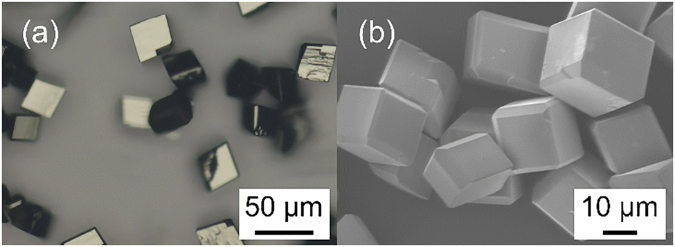 | ||
| Fig. 1 (a) Optical micrograph and (b) SEM image of rhombohedral shaped C70 crystals grown from a C70-m-xylene solution. | ||
Results and discussion
Solution-grown C70 crystals
To determine the structure and composition of C70 crystals with rhombohedral shapes, many crystals were grown using the solvent evaporation method. The crystals obtained had rhombohedral shapes with clear crystal habits (Fig. 1), although the size and number of crystals depended on the amount and temperature of the solution and the evaporation time. Fig. S5 (ESI†) shows optical micrographs of C70 crystals from different saturated solutions prepared at 5 °C, 20 °C and 40 °C, respectively. C70 crystals with two types of shapes such as rhombohedral and needle shapes were obtained. The ratio of the two shapes depends on the saturated solution. The ratio of rhombohedral crystals was predominant using the saturated solution prepared at a lower temperature of 5 °C, while needle crystals were predominant using the saturated solution prepared at a higher temperature of 40 °C. The rhombohedral crystals which are stable and of high quality were used in this work. Regardless of the size and number of rhombohedral crystals, they had the same crystal structure and chemical composition.The chemical composition of the solution-grown C70 crystals with rhombohedral shapes was confirmed by FT-IR spectroscopy. Fig. 2(a) shows the FT-IR spectra around 600–1500 cm−1 for the solution-grown crystals after drying in air for one day and after annealing at 100 °C under 3.0–4.0 × 10⁻³ Pa for 11 days. The FT-IR spectra of m-xylene used as the solvent and the sublimation-grown C70 crystals including no solvent are also shown in the figure. Many peaks in the solution-grown C70 crystals are observed in the sublimation-grown C70 crystals, which are associated with the vibrational modes of the C70 molecules.26,27 In contrast, some peaks indicated by filled triangles in Fig. 2(a) are not observed in the sublimation-grown C70 crystals but correspond to those in m-xylene. These peaks are associated with the vibrational modes of m-xylene. The solution-grown C70 crystals thus comprise C70 and m-xylene, which suggests a solvated structure.
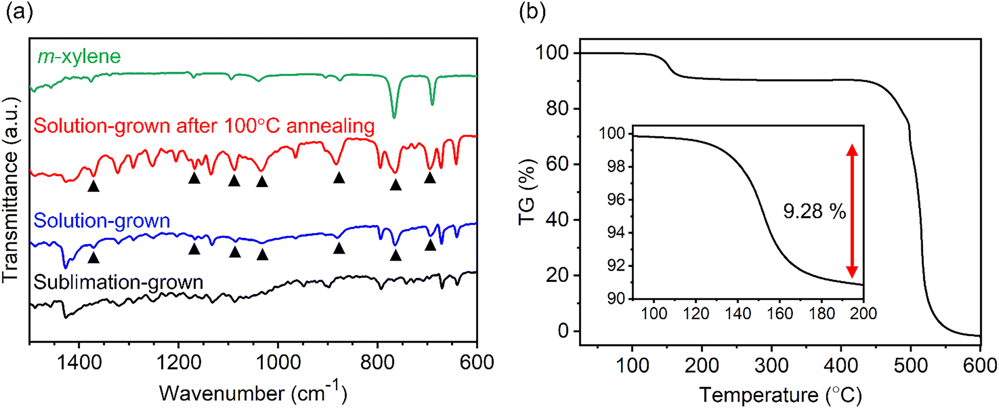 | ||
| Fig. 2 (a) Blue and red lines show the FT-IR spectra after drying C70 crystals with rhombohedral shapes grown from a C70-m-xylene solution in air for one day and after annealing them at 100 °C for 11 days under 3.0–4.0 × 10⁻³ Pa, respectively. For reference, the FT-IR spectra of sublimation-grown C70 crystals without a solvent and m-xylene as the solvent are also shown in the figure. The peaks corresponding to those of m-xylene are indicated by filled triangles. (b) TG curve of C70 crystals with rhombohedral shapes grown from C70-m-xylene solution. The inset shows an enlarged view in the temperature range from 90 °C to 200 °C. The TG curve was recorded at a heating rate of 10 °C min−1 in air. | ||
The FT-IR peaks of the solution-grown crystals were shifted by 2–4 cm−1 compared to those of the sublimation-grown crystals and m-xylene. The slight shift reflects the intermolecular interaction between the C70 molecules and the m-xylene molecules, as previously reported for C60 solvated crystals.28 In addition, the FT-IR peaks in the solution-grown crystals composed of C70 and m-xylene remained almost unchanged even after annealing at 100 °C in a vacuum. This indicates that the solvated structures of C70 and m-xylene were preserved under the annealing conditions used in this study.
TG measurements were performed to better understand the chemical composition of the solution-grown C70 crystals with rhombohedral shapes. Fig. 2(b) shows the TG curves of the solvated C70 crystals in air. Weight losses were observed at 140–165 °C and 491–532 °C, which can be related to the desorption of m-xylene and sublimation of C70 molecules, in the solvated C70 crystals, respectively. The desorption temperature of 140–165 °C of m-xylene is consistent with the fact that the m-xylene-solvated structure is retained even upon annealing at 100 °C as is evident in the FT-IR spectra of Fig. 2(a).
The weight loss corresponding to the desorption of m-xylene was approximately 9.28% (Fig. 2(b)). Assuming the aforementioned weight loss and molecular weights of 840.77 and 106.17 of C70 and m-xylene, respectively, the composition ratio of C70 and m-xylene in the solvated C70 crystals with rhombohedral shapes is estimated to be approximately 10![[thin space (1/6-em)]](https://www.rsc.org/images/entities/char_2009.gif) :8. The composition ratio was similar to that of solvated C70 needle crystals grown by the liquid–liquid interfacial precipitation method with two types of solvents, m-xylene and IPA, as reported previously.23,29 This indicates that the crystal morphology changes considerably depending on the growth method, even if the crystals have almost the same solvent composition ratio. The slight discrepancy in the solvation ratio could be related to crystal morphologies, such as needle and rhombohedral shapes.
:8. The composition ratio was similar to that of solvated C70 needle crystals grown by the liquid–liquid interfacial precipitation method with two types of solvents, m-xylene and IPA, as reported previously.23,29 This indicates that the crystal morphology changes considerably depending on the growth method, even if the crystals have almost the same solvent composition ratio. The slight discrepancy in the solvation ratio could be related to crystal morphologies, such as needle and rhombohedral shapes.
The XRD patterns of the solution-grown C70 crystals with rhombohedral shapes are shown in Fig. 3. For reference, the XRD pattern of the sublimation-grown C70 crystals is also shown in this figure. The PXRD pattern of the sublimation-grown crystals can be explained in terms of two types of crystal forms: the rhombohedral form with a = 10.15 Å and c = 27.95 Å and the hexagonal form with a = 10.16 Å and c = 18.6 Å.
 | ||
| Fig. 3 PXRD patterns of C70 crystals with rhombohedral shapes grown from C70-m-xylene solution. (a) and (b) XRD patterns after drying them in air for one day and after annealing them at 100 °C for 11 days under 3.0–4.0 × 10⁻³ Pa, respectively. As a reference, the XRD patterns of sublimation-grown C70 crystals without the solvent is also shown as (c) in the figure. The XRD pattern of sublimation-grown C70 crystals is understood by using those in two kinds of crystal forms such as rhombohedral (denoted as r) and hexagonal (denoted as h) forms. | ||
The difference between the two crystal forms is related to changes in the stacking order of the crystal planes. These crystal forms are also in good agreement with those previously reported.30–32
The pattern of solution-grown C70 crystals with rhombohedral shapes is clearly different from that of sublimation-grown C70 crystals. It is assigned to the hexagonal structure with lattice constants of a = 50.3013 Å and c = 24.5686 Å. This was also confirmed by SCXRD measurements. Notably, the XRD pattern remains unchanged even after annealing at 100 °C. This indicates that the hexagonal solvated structure is maintained even after annealing at 100 °C. Thus, the behavior of the XRD pattern is consistent with that of the FT-IR and TG results.
Directly grown C70 crystal FETs
Fig. 4(a) shows an SEM image of a C70 single crystal with rhombohedral shapes grown directly on the FET substrate (direct-growth C70 crystal FETs), which was used for the FET measurements in this study. The channel length L and the channel width W of the FET are estimated to be 23.1 μm and 26.1 μm, respectively (Fig. 4(a)). | ||
| Fig. 4 (a) SEM image of a C70 crystal with a rhombohedral shape grown directly on and the electrode FET substrate from a C70-m-xylene solution. Typical (b) output and (c) transfer characteristics of direct growth C70 crystal FETs before annealing in a vacuum, as measured at 27 °C. | ||
An optical microscopy (OM) image of the direct-growth C70 crystal FET is shown in Fig. S6 (ESI†). 75% of the obtained rhombohedral crystals were grown to bridge the two electrodes on the substrate. In addition, the growth direction to bridge the two electrodes was always a defined crystallographic direction as shown in Fig. 4(a) and Fig. S6 (ESI†). The size distribution of the C70 crystals grown to bridge the two electrodes is shown in Fig. S7(a) and (b) (ESI†), where the sizes correspond to the diagonal lengths (short and long) in the obtained crystal morphology as shown in Fig. S7(c) (ESI†). The short diagonal length, which corresponds to the bridge between the two electrodes, was relatively uniform with a size of 51.0 ± 8.80 μm. For FET measurements, some rhombohedral crystals that bridged the two electrodes securely were left on the substrate, while others that bridged the two electrodes fairly well were removed from the substrate. To evaluate mobility, the channel width (W) of all residual crystals bridging the two electrodes was measured from SEM images, as shown in Fig. 4(a).
Fig. 4(b) shows the output characteristics of the vacuum-dried FET. The source–drain current (IDS) increases linearly with the source–drain voltage (VDS) up to approximately VDS = 15 V and approaches a constant maximum value. The transfer characteristics at VDS = 40 V also exhibit good gate modulation with respect to the gate voltage (VG) (Fig. 4(c)). The output and transfer characteristics show typical n-type FET behavior. Analysis of the transfer characteristics at VDS = 40 V (Fig. 4(c)) shows that the electron mobility (μ), threshold voltage (VT) and on/off ratio (Ion/Ioff) of the direct growth C70 crystal FET are estimated to be 1.19 × 10⁻³ cm2 V−1 s−1, 15.9 V, and 39.6, respectively. Thus, the transport properties of the direct-growth C70 crystal FETs were successfully characterized.
The transport properties of C60 and C70 crystals are known to deteriorate significantly due to the adsorption of H2O and O2 in the crystals; however, these species can be desorbed by annealing at approximately 100 °C.33,34 To remove the H2O and O2 adsorbed in the C70 crystals, the FET devices were annealed at 100 °C under 3.0–4.0 × 10⁻³ Pa for 25 days. Notably, the m-xylene in the solvated C70 crystals remains in the crystals even after vacuum-annealing at 100 °C, as the desorption of m-xylene requires a higher temperature of 140–165 °C, as shown in the FT-IR and TG results. The electron mobility in the direct growth C70 crystal FETs increased significantly by vacuum-annealing at 100 °C. This indicates that the increase in electron mobility is attributed to the desorption of H2O and O2 by vacuum-annealing at 100 °C, as previously reported for C60 and C70 crystals.7,23
In addition, the effect of m-xylene in the solvated crystals is of interest for higher mobility. Evaporation of the solvent by heat-treatment at a higher temperature of 200 °C could lead to experimental evidence of solvent effects for solvated crystal FETs. However, heat treatment not only evaporates the solvent but also leads to the degradation of crystallinity with a change in the crystal structure as has already been observed for C70 needle crystals.23 Therefore, it is difficult to accurately measure the solvent effect or pure C70 crystal FETs.
Fig. 5(a) shows the relationship between the electron mobility of the directly grown C70 crystal FETs and the number of days they were annealed at 100 °C in a vacuum, where the values of the electron mobilities were measured at 100 °C. The electron mobility increased and approached a constant maximum value as the number of days of annealing increased. The maximum value of mobility was 1.50 cm2 V−1 s−1 after 25 days of annealing at 100 °C.
 | ||
| Fig. 5 (a) Increase in the electron mobility of direct growth C70 crystal FETs as a function of the number of days they were annealed at 100 °C under 3.0–4.0 × 10⁻³ Pa. Vacuum annealing leads to the desorption of H2O and O2 absorbed in the crystals. Typical (b) output and (c) transfer characteristics of direct growth C70 crystal FETs after annealing at 100 °C under 3.0–4.0 × 10⁻³ Pa for 25 days, as measured at 27 °C. | ||
It is assumed that the mobility value reaches a constant maximum value after 25 days of annealing, although further annealing could lead to a slight increase in mobility. In fact, the dependence of the slope  of the transfer characteristics, which is used to evaluate the mobility, on the number of annealing days was well-fitted with an exponential curve as shown in Fig. S8 (ESI†). After fitting, the constant maximum value of mobility is evaluated as 1.59 cm2 V−1 s−1, which is slightly higher than the value after 25 days of annealing. A similar behavior of mobility as a function of the number of days of annealing was also observed for other samples with rhombohedral crystals. The saturation of mobility occurs in all samples after more than 20 days of annealing, where O2 and H2O in the crystals are completely removed by annealing. The evaporation rate of O2 and H2O is high in smaller crystals as the specific surface area is large in smaller crystals. More than 20 days of annealing for rhombohedral crystals is clearly longer than 9 days for smaller needle crystals reported previously.23 Thus, the days of annealing leading to mobility saturation depend on the crystal size, i.e., the specific surface area.
Fig. 5(b) and (c) show the output and transfer characteristics of the direct growth C70 crystal FETs at 27 °C after annealing at 100 °C under 3.0–4.0 × 10⁻³ Pa for 25 days. The current values of the μA orders increase sharply compared to the nA orders before annealing as shown in Fig. 4(b). According to previous studies on C70 needle-crystal FETs with poor electrical contact between crystals and electrodes, in the output characteristics, IDS increased non-linearly and slowly with VDS in the low voltage range.25 In addition, no current saturation was observed even at high VDS. This behavior may be attributed to poor contact or non-ohmic contact between the C70 crystal and the FET substrate with the electrodes. In the direct-growth C70 crystal FETs measured in this study, the non-ohmic behavior was largely improved so that ideal and excellent output characteristics, including the linear and saturation regions, were clearly observed (Fig. 5(b)). The electron mobility, VT and Ion/Ioff of the direct growth C70 crystal FETs after annealing are estimated to be 1.14 cm2 V−1 s−1, 21.1 V and 6.75 × 10⁴, respectively, as measured at 27 °C. The electron mobility increased by three orders of magnitude compared to that before annealing.
The electron mobility, VT, and Ion/Ioff for fullerene-based OFETs with C60 are summarized in Table 1. The electron mobility of the direct-growth C70 crystal FETs measured in this study exhibits the highest value compared to those of OFETs based on C70 as previously reported.20–23 The electron mobility value is also comparable to that of top-contact C60 based FETs, which correspond to the highest performance in n-type OFETs.
| Configuration | μ (cm2 V−1 s−1) | V T (V) | I on/Ioff | Ref. | ||
|---|---|---|---|---|---|---|
| C60 | Thin film | Bottom contact | 8.00 × 10⁻² | 15.0 | 1.09 × 10⁶ | 1 |
| 5.60 × 10⁻¹ | 17.0 | >108 | 3 | |||
| 6.50 × 10⁻¹ | 32.0 | >106 | 4 | |||
| 2.00 × 10⁻¹ | — | — | 5 | |||
| 3.23 | 17.1 | 4.00 × 10⁶ | 6 | |||
| Top contact | 4.90 | — | — | 12 | ||
| 6.00 | — | — | 5 | |||
| 4.30 | <1.00 | >106 | 13 | |||
| Crystal | Bottom contact | 3.00 × 10⁻² | 3.30 × 10⁻¹ | 1.35 × 10² | 7 | |
| 2.00 × 10⁻² | 0 | — | 8 | |||
| ∼ 10−2 | −13.0 | ∼ 102 | 9 | |||
| 2.00 × 10⁻³ | — | — | 10 | |||
| 3.82 × 10⁻² | — | — | 11 | |||
| Top contact | 11.1 | 28.0 | 2.50 × 10⁶ | 14 | ||
| 2.00 ± 0.61 | 36.0 ∼ 85.0 | >106 | 15 | |||
| 2.30 | 16.5 | 2.40 × 10⁴ | 16 | |||
| 5.09 | 6.60 × 10⁻¹ | 105–106 | 17 | |||
| C70 | Thin film | Bottom contact | 2.00 × 10⁻³ | 27.0 | — | 2 |
| 6.60 × 10⁻² | 40.0 | >105 | 4 | |||
| Crystal | Bottom contact | 6.00 × 10⁻⁵ | — | — | 22 | |
| 1.32 × 10⁻² | 9.64 | 64.0 | 23 | |||
| 8.20 × 10⁻⁵ | — | — | 20 | |||
| ∼10−5 | — | — | 21 | |||
| 1.14 | 17.2 | 7.84 × 10⁴ | This work | |||
The electron mobility values after annealing for 25 days were 1.50 cm2 V−1 s−1 at 100 °C and 1.14 cm2 V−1 s−1 at 27 °C, indicating that the mobility increases with temperature. This behaviour suggests that electron transport in the C70 crystals follows a hopping conduction mechanism associated with thermal activity, which is a typical conduction mechanism in molecular crystals.
In previous studies on C70 needle-crystal FETs, the electron mobility was estimated from the transfer characteristics, assuming negligible contact resistance between the C70 crystal and the S/D electrodes on the substrate. However, if the contact resistance is significant, this may result in reduced current values, possibly leading to an underestimation of electron mobility. In contrast, in this study, the contact was significantly improved, minimizing the limit of the injection current and allowing a more accurate estimation of the intrinsic electron mobility.
Conclusions
In this study, high-mobility FETs fabricated by the direct growth of C70 crystals from C70 saturated m-xylene solution have been demonstrated. Good electrical contact between the C70 crystals and FET substrates was realized with electrodes in the bottom-gated bottom-contact FET configuration. The C70 crystals obtained exhibit rhombohedral shapes with solvated hexagonal structures. Directly grown C70 crystal FETs exhibit typical n-type output and transfer characteristics. The electron mobility increases with annealing at 100 °C in a vacuum, leading to the desorption of H2O and O2 in the crystals, although solvation in the crystals is maintained. The solvated C70 crystal FETs have a high electron mobility of 1.14 cm2 V−1 s−1 which is an improvement of more than two orders of magnitude compared to the previously reported C70 FETs. The electron mobility value was also comparable to that of the electron mobility in top-contact C60 based FETs, which corresponds to the highest mobility in n-type OFETs. This shows the potential application of C70 crystals in electronic devices. It is anticipated that more advanced solution-processing techniques developed for organic crystalline FETs24,25 will be employed in the fabrication of high-mobility C70 FETs for practical applications.Author contributions
Yuto Sakai: data curation, formal analysis, investigation, methodology, validation, visualization, writing review, and editing. Taiyo Araki: data curation, formal analysis, investigation, methodology, validation, visualization, writing review, and editing. Ryo Suzuki: data curation, formal analysis, funding acquisition, visualization, writing review, and editing. Toshiyuki Sasaki: data curation, formal analysis, visualization, writing review, and editing. Kouhei Ichiyanagi: data curation, formal analysis, visualization, writing review, and editing. Tadahiko Hirai: formal analysis, visualization, writing review, and editing. Nobuyuki Aoki: resources (FET devices), writing review, and editing. Masaru Tachibana: conceptualization, project administration, supervision, funding acquisition, writing – original draft, writing – review, and editing.Conflicts of interest
There are no conflicts to declare.Data availability
The data supporting this article have been included as part of the ESI.†Acknowledgements
We thank Mr Ken Inoue from Yokohama City University for his assistance in the preparation of this manuscript. We also thank Prof. Genji Kurisu, Dr Takanori Nakane, and Dr Akihiro Kawamoto from the Institute for Protein Research, Osaka University, Dr Naruhiko Adachi from the University of Tsukuba, Dr Yusuke Yamada from Tohoku University, and Dr Haruki Sugiyama from the Comprehensive Research Organization for Science and Society. The XRD measurements were performed at BL40XU and BL41XU at SPring-8 with the approval of JASRI (Proposal no. 2023B2429, 2023B2432, 2024A1112, and 2024A1142). This work was supported by PRESTO, Japan Science and Technology Agency (JPMJPR1995), and Japan Society for the Promotion of Science (JSPS) KAKENHI Grants-in-Aid for Scientific Research (Grant No. 19K23579, 23H01305, 23K26000, and 25K08281). This research was partially supported by the Research Support Project for Life Science and Drug Discovery (Basis for Supporting Innovative Drug Discovery and Life Science Research (BINDS)) from AMED under Grant Number JP24ama121001 (support number 6707).References
- R. C. Haddon, A. S. Perel, R. C. Morris, T. T. M. Palstra, A. F. Hebard and R. M. Fleming, Appl. Phys. Lett., 1995, 67, 121–123 CrossRef CAS.
- R. C. Haddon, J. Am. Chem. Soc., 1996, 118, 3041–3042 CrossRef CAS.
- S. Kobayashi, T. Takenobu, S. Mori, A. Fujiwara and Y. Iwasa, Appl. Phys. Lett., 2003, 82, 4581–4583 CrossRef CAS.
- J. N. Haddock, X. Zhang, B. Domercq and B. Kippelen, Org. Electron., 2005, 6, 182–187 CrossRef CAS.
- T. D. Anthopoulos, B. Singh, N. Marjanovic, N. S. Sariciftci, A. M. Ramil, H. Sitter, M. Cölle and D. M. de Leeuw, Appl. Phys. Lett., 2006, 89, 213504 CrossRef.
- M. Kitamura, S. Aomori, J. H. Na and Y. Arakawa, Appl. Phys. Lett., 2008, 93, 033313 CrossRef.
- A. L. Briseno, S. C. B. Mannsfeld, M. M. Ling, S. Liu, R. J. Tseng, C. Reese, M. E. Roberts, Y. Yang, F. Wudl and Z. Bao, Nature, 2006, 444, 913–917 CrossRef CAS PubMed.
- K. Ogawa, T. Kato, A. Ikegami, H. Tsuji, N. Aoki, Y. Ochiai and J. P. Bird, Appl. Phys. Lett., 2006, 88, 112109 CrossRef.
- Y. Ochiai, K. Ogawa, N. Aoki and J. P. Bird, J. Phys.:Conf. Ser., 2009, 159, 012004 CrossRef.
- D. Mahdaoui, C. Hirata, K. Nagaoka, K. Miyazawa, K. Fujii, T. Ando, M. Abderrabba, O. Ito, M. Takagi, T. Ishimoto, M. Tachikawa, S. Yagyu, Y. Liu, Y. Nakajima, Y. Nemoto, K. Tsukagoshi and T. Wakahara, J. Mater. Chem. C, 2022, 10, 3770–3774 RSC.
- T. Wakahara, C. Hirata, D. Mahdaoui, K. Fujii, Y. Matsushita, O. Ito, M. Takagi, T. Shimazaki, M. Tachikawa, S. Yagyu, Y. Liu, Y. Nakajima, T. Nagai and K. Tsukagoshi, Carbon, 2025, 233, 119838 CrossRef CAS.
- K. Itaka, M. Yamashiro, J. Yamaguchi, M. Haemori, S. Yaginuma, Y. Matsumoto, M. Kondo and H. Koinuma, Adv. Mater., 2006, 18, 1713–1716 CrossRef CAS.
- X. H. Zhang and B. Kippelen, J. Appl. Phys., 2008, 104, 104504 CrossRef.
- H. Li, B. C. K. Tee, J. J. Cha, Y. Cui, J. W. Chung, S. Y. Lee and Z. Bao, J. Am. Chem. Soc., 2012, 134, 2760–2765 CrossRef CAS PubMed.
- H. Li, C. Fan, M. Vosgueritchian, B. C.-K. Tee and H. Chen, J. Mater. Chem. C, 2014, 2, 3617–3624 RSC.
- X. Zhao, T. Liu, Y. Cui, X. Hou, Z. Liu, X. Dai, J. Kong, W. Shi and T. J. S. Dennis, Nanoscale, 2018, 10, 8170–8179 RSC.
- Z. Lu, W. Deng, X. Fang, J. Xiao, B. Lu, X. Zhang, A. A. A. Pirzado, J. Jie and X. Zhang, Adv. Funct. Mater., 2021, 31, 2105459 CrossRef CAS.
- P. Hu, X. He and H. Jiang, InfoMat, 2021, 3, 613–630 CrossRef CAS.
- S. Arabnejad, A. Pal, K. Yamashita and S. Manzhos, Front. Energy Res., 2019, 7, 00003 CrossRef.
- T. Wakahara, K. Nagaoka, C. Hirata, K. Miyazawa, K. Fujii, Y. Matsushita, O. Ito, M. Takagi, T. Shimazaki, M. Tachikawa, Y. Wada, S. Yagyu, Y. Liu, Y. Nakajima and K. Tsukagoshi, RSC Adv., 2022, 12, 19548–19553 RSC.
- D. Mahdaoui, C. Hirata, K. Nagaoka, K. Miyazawa, K. Fujii, T. Ando, M. Abderrabba, O. Ito, S. Yagyu, Y. Liu, Y. Nakajima, K. Tsukagoshi and T. Wakahara, Nanomaterials, 2023, 13, 2469 CrossRef CAS PubMed.
- D. Mahdaoui, C. Hirata, K. Nagaoka, K. Miyazawa, K. Fujii, T. Ando, Y. Matsushita, M. Abderrabba, O. Ito, K. Tsukagoshi and T. Wakahara, Diamond Relat. Mater., 2022, 128, 109217 CrossRef CAS.
- Y. Mitake, A. Gomita, R. Yamamoto, M. Watanabe, R. Suzuki, N. Aoki, M. Tanimura, T. Hirai and M. Tachibana, Chem. Phys. Lett., 2022, 807, 140094 CrossRef CAS.
- S. Chen, Z. Li, Y. Qiao and Y. Song, J. Mater. Chem. C, 2021, 9, 1126–1149 RSC.
- Z. Chen, S. Duan, X. Zhang and W. Hu, Mater. Chem. Front., 2024, 8, 2227–2272 RSC.
- R. A. Jishi, M. S. Dresselhaus, G. Dresselhaus, K. A. Wang, P. Zhou, A. M. Rao and P. C. Eklund, Chem. Phys. Lett., 1993, 206, 187–192 CrossRef CAS.
- K. Thirunavukkuarasu, V. C. Long, J. L. Musfeldt, F. Borondics, G. Klupp, K. Kamarás and C. A. Kuntscher, J. Phys. Chem. C, 2011, 115, 3646–3653 CrossRef CAS.
- Y. Funamori, R. Suzuki, T. Wakahara, T. Ohmura, E. Nakagawa and M. Tachibana, Carbon, 2020, 169, 65–72 CrossRef CAS.
- M. Watanabe, A. Gomita, R. Suzuki and M. Tachibana, Carbon Trends, 2023, 10, 100246 CrossRef CAS.
- M. A. Verheijen, H. Meekes, G. Meijer, P. Bennema, J. L. de Boer, S. van Smaalen, G. van Tendeloo, S. Amelinckx, S. Muto and J. van Landuyt, Chem. Phys., 1992, 166, 287–297 CrossRef CAS.
- G. B. M. Vaughan, P. A. Heiney, D. E. Cox, J. E. Fischer, A. R. McGhie, A. L. Smith, R. M. Strongin, M. A. Cichy and A. B. Smith, Chem. Phys., 1993, 178, 599–613 CrossRef CAS.
- J. Janaki, G. V. N. Rao, V. S. Sastry, Y. Hariharan, T. S. Radhakrishnan, C. S. Sundar, A. Bharati, M. C. Valsakumar and N. Subramanian, Solid State Commun., 1995, 94, 37–40 CrossRef CAS.
- T. Arai, Y. Murakami, H. Suematsu, K. Kikuchi, Y. Achiba and I. Ikemoto, Solid State Commun., 1992, 84, 827–829 CrossRef CAS.
- A. Tapponnier, I. Biaggio and P. Günter, Appl. Phys. Lett., 2005, 86, 112114 CrossRef.
Footnote |
| † Electronic supplementary information (ESI) available. See DOI: https://doi.org/10.1039/d5tc01627d |
| This journal is © The Royal Society of Chemistry 2025 |