
 Open Access Article
 This Open Access Article is licensed under a
 Creative Commons Attribution 3.0 Unported Licence
Thermoelectric properties and figure of merit of Cu2ZnSnS4†
Tooba Sajid ,
Joseph M. Flitcroft,
Robert Freer,
David J. Lewis and
Jonathan M. Skelton*
,
Joseph M. Flitcroft,
Robert Freer,
David J. Lewis and
Jonathan M. Skelton*
Department of Chemistry, University of Manchester, Oxford Road, Manchester M13 9PL, UK. E-mail: jonathan.skelton@manchester.ac.uk
First published on 10th July 2025
Abstract
Thermoelectric (TE) power is a leading technology for addressing energy waste, and the quaternary sulphide Cu2ZnSnS4 (CZTS) is of considerable interest for lightweight and flexible thin-film devices. However, the large variation in the figure of merit, ZT, obtained in experimental studies highlights the need for a more comprehensive characterisation of the material properties. In this work, we apply a fully ab initio modelling approach to obtain high-quality reference predictions of the thermoelectric properties and ZT of CZTS. We find that CZTS has large bulk κlatt, due to long phonon lifetimes, which can be minimised by nanostructuring. We predict significantly higher electrical conductivity, Seebeck coefficients and power factors with p-type (hole) doping compared to n-type (electron) doping. The electrical properties are less sensitive to crystallite size than the κlatt, and we predict an industry-standard high-temperature ZT > 1 should be achievable for nanostructured p-type CZTS with crystallite sizes below 10 nm. Comparing our predictions to measurements also suggests that modelling heavily-doped CZTS or CZTS-based solid solutions may yield valuable insight into how the ZT can be optimised further.
1 Introduction
The world has historically responded to increasing demand for energy by burning fossil fuels. However, fossil fuels are a finite resource, and fossil-fuel derived energy produces greenhouse gas emissions that contribute heavily to anthropogenic climate change. There is therefore a pressing need to switch to clean and renewable sources of energy. Over 60% of the energy produced globally is lost as heat,1 and improving the efficiency of energy-intensive processes is therefore a key enabler of the clean-energy transition.Recovering waste heat to electricity using thermoelectric power is a promising approach to addressing energy waste.2 Thermoelectric generators (TEGs) are solid-state devices that extract electrical energy from a temperature gradient.3 TEGs have no mechanical components and are thus easy to maintain, and do not produce any noise, heat, chemical waste or greenhouse gases during operation.4,5 TEGs have proven applications in the aerospace industry, and can potentially be scaled to a wide range of applications from powering small devices (e.g. pacemakers), to improving the efficiency of automobile engines, to heat recovery from large industrial facilities.6–8 The market for thermoelectric energy harvesting was valued at US $320 m in 2017 and is forecast to increase to $1.5 bn by 2028.2
TEGs utilise the Seebeck effect in a thermoelectric (TE) material, where a temperature difference induces a potential difference quantified by the Seebeck coefficient S:3
 | (1) |
Positive and negative S indicate dominant p-type (hole) and n-type (electron) carriers, respectively, and a working TEG requires materials of both type to form a couple. The efficiency of a TE material can be defined by the dimensionless figure of merit ZT:2
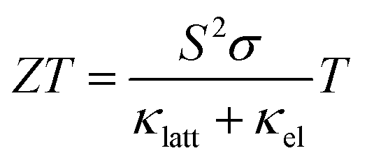 | (2) |
There is a strong correlation between the electrical properties S, σ and κel through the carrier concentration n, which makes maximising the ZT challenging.8,10,11 Increasing n increases the σ, but may also increase the κel and degrade the S. The n should therefore be optimised to maximise the PF but without significantly increasing the electronic thermal conductivity. On the other hand, the κlatt is largely independent of the electronic structure but is linked to the crystal structure, chemical bond strength, and structural dynamics.8,12 All four properties in the ZT equation are also temperature dependent, and, in particular, the κlatt typically falls sharply with T, resulting in many TE materials performing best at high temperature.
Current high-performance TE materials include PbTe, with a ZT of up to ∼2.2 at 915 K,13 and Bi2Te3, with a ZT of up to 1.35 from 300–400 K.14 Bi2Te3 is commonly used for the dual application of solid-state refrigeration, while PbTe has been used in aerospace applications.15,16 Due to the scarcity of tellurium and toxicity of lead, which limit scalability, increase costs, and potentially cause problems with end-of-life disposal, there has been significant research into earth-abundant, non-toxic alternatives. Metal chalcogenide systems often show the required balance of favourable electrical properties and intrinsically-low κlatt.2,10,17 For example, orthorhombic SnSe has a high-temperature bulk ZT of up to 2.6,18,19 which can be increased to ZT ≈ 3 in polycrystalline samples.20 More complex quaternary chalcogenides have also shown potential as high-performance TEs due to the possibility of low κlatt,21–24 particularly when used in nanoparticulate or thin-film forms.21,23
Among these, the quaternary metal chalcogenide Cu2ZnSnS4 (CZTS) is well known as a thin-film photovoltaic material,25,26 and has recently attracted attention as a prospective TE due to its abundant constituents, low toxicity, and low cost.27 However, studies on pristine CZTS have thus far indicated performance well short of the ZT ≥ 1 required to be industrially viable. For example, Yang et al. and Liu et al. reported maximum ZT of 0.026 and 0.039 at 700 K, respectively, for CZTS nanocrystals and consolidated powders.12,28 This modest performance can be improved substantially through chemical doping. For example, Nagaoka et al. achieved a very large ZT = 1.6 at 800 K in Na-doped CZTS single crystals,29 while Liu et al. found that substituting Zn with Fe and Cd in CZTS thin films yielded a significant improvement in the PF and an estimated maximum ZT of 0.18–0.69 at 550 K.30 The latter result is particularly interesting given that thin-film TEs require less material, which reduces costs, and have the advantages of being lightweight and flexible.31,32 From a performance perspective, thin films can also show high ZT through a reduction in the κlatt due to the boundary scattering introduced by small crystallite sizes.8,33
Despite these successes in preparing and characterising CZTS-based TEs, the considerable variation in experimental studies highlights the need for an improved understanding of the intrinsic TE properties of CZTS and the level of doping and nanostructuring required to optimise its performance. We have recently developed a fully ab initio workflow for predicting the thermoelectric properties and ZT, which we have tested against multiple classes of TE materials including chalcogenides and oxychalcogenides.34–36 In this work, we apply our methodology to obtain high-quality reference predictions for the properties and ZT of pristine CZTS as a function of temperature and doping level. Our modelling indicates that p-type CZTS should show improved electrical properties and higher ZT compared to the n-doped material. We predict a relatively large κlatt of 9.4 W m−1 K−1 at 300 K, which can be reduced by as much as 80% by nanostructuring to the ∼10 nm crystallite size reported in some experiments on thin films. On the other hand, the electrical properties are much less sensitive to nanostructuring, and we predict a maximum ZT, ZTmax, of 1.01 at 1000 K for p-type CZTS with a crystallite size of 10 nm. This is more than double the bulk ZTmax = 0.45, and can be increased by ∼25% with a further reduction of the crystallite size to 5 nm. This indicates that targeting thin films with small crystallite sizes and/or exploring other techniques such as defect engineering to minimise the κlatt should provide a facile route to maximising the ZT of CZTS-based TEs.
2 Methodology
Calculations on bulk CZTS were performed using pseudopotential plane-wave density-functional theory (DFT) with the Vienna Ab initio Simulation Package (VASP) code.37Electron exchange and correlation were modelled using the PBEsol exchange–correlation functional.38 The ion cores were modelled using projector augmented-wave (PAW) pesudopotentials39,40 with valence configurations of: Cu – 3d104s1; Zn – 3d104s2; Sn – 5s25p2; and S – 3s23p4. Explicit convergence testing determined that a plane-wave cutoff of 600 eV for the valence electrons, in conjunction with Γ-centered 3 × 3 × 4 and 4 × 4 × 1 Monkhorst–Pack k-point grids41 for the primitive and conventional cells, respectively, was sufficient to converge the total energy to <1 meV atom−1 and the external pressure to <1 kbar.
The initial structure of CZTS in the kesterite phase was obtained from the materials project,42 symmetrised using spglib,43 and fully optimised to tight tolerances of 10−8 eV and 10−2 eV Å−1 on the electronic total energy and ionic forces, respectively. When required, the following transformation matrix was used to convert from the conventional to the primitive cell:
 | (3) |
The second-order and third-order force constants (harmonic/anharmonic FCs) were determined using the supercell finite-displacement method implemented in the Phonopy and Phono3py codes.44,45 The harmonic FCs were computed from a 4 × 4 × 2 expansion of the conventional unit cell with 512 atoms and a displacement step of 10−2 Å. An atom-projected phonon density of states (PDoS) curve was obtained by interpolating the phonon frequencies onto a uniform Γ-centered q-point mesh with 12 × 12 × 12 subdivisions and using the linear tetrahedron method for Brillouin zone (BZ) integration. A phonon dispersion (band structure) was obtained by interpolating the frequencies along strings of q-points passing through all the high-symmetry points in the tetragonal I![[4 with combining macron]](https://www.rsc.org/images/entities/char_0034_0304.gif) BZ. The anharmonic FCs were determined in a 2 × 2 × 1 expansion of the conventional unit cell with 64 atoms and a step size of 3 × 10⁻² Å. The third-order FCs were used in conjunction with the harmonic phonon frequencies and eigenvectors to determine the phonon linewidths and lifetimes using perturbation theory.45 The phonon lifetimes were then combined with the harmonic modal heat capacities and group velocities to calculate the lattice thermal conductivity within the single-mode relaxation time approximation (SM-RTA), with modal properties evaluated on a 12 × 12 × 12 q-point mesh.45
BZ. The anharmonic FCs were determined in a 2 × 2 × 1 expansion of the conventional unit cell with 64 atoms and a step size of 3 × 10⁻² Å. The third-order FCs were used in conjunction with the harmonic phonon frequencies and eigenvectors to determine the phonon linewidths and lifetimes using perturbation theory.45 The phonon lifetimes were then combined with the harmonic modal heat capacities and group velocities to calculate the lattice thermal conductivity within the single-mode relaxation time approximation (SM-RTA), with modal properties evaluated on a 12 × 12 × 12 q-point mesh.45
The three electrical properties, viz. the Seebeck coefficient, electrical conductivity and electronic thermal conductivity, were calculated using the AMSET code.46
An accurate electronic bandgap was obtained using the HSE06 hybrid functional47 and used to correct an electronic band structure obtained using PBEsol on a uniform k-point mesh with 2× the number of points as that used for the geometry optimisation. This k-point sampling was subsequently increased by a factor of ∼20× using Fourier interpolation during the transport calculations.
The electron scattering rates were estimated for four mechanisms, viz. acoustic-deformation potential (ADP), polar-optic phonon (POP), ionised impurity (IMP) and piezoelectric (PIE) scattering, requiring the calculation of a number of additional materials properties. The acoustic deformation potentials were calculated from single-point calculations on deformed structures generated using AMSET. The high-frequency dielectric constant ε∞ and atomic Born effective charges Z* were calculated using density-functional perturbation theory (DFPT).48 The Γ-point phonon frequencies, the elastic constants Cij, the ionic contribution to the dielectric constant εionic, and the piezoelectric tensor elements e(0)ij were determined using a combination of the DFPT and finite-difference routines in VASP. Finally, the static dielectric constant εS was then calculated as εS = ε∞ + εionic, and the phonon frequencies and Z* were used to calculate the polar-optic phonon frequency ωpo.
3 Results and discussion
3.1 Structure and phonon spectra
Kesterite CZTS crystallises in the tetragonal I spacegroup (no. 82) with sixteen atoms in the conventional unit cell (Fig. 1).
 | ||
| Fig. 1 Optimised structure of Cu2ZnSnS4 obtained in this work. Atom colors: Cu – blue; Zn – grey; Sn – orange; S – yellow. This image was prepared using the VESTA software.49 | ||
Our optimized lattice parameters are compared to experimental measurements50–53 and previous calculations54–57 in Table S1 (ESI†). The calculated lattice constants a = b and c are within ∼1% of the measurements, and the calculated volume V is within 2–3%. Given that our optimized structures are “athermal”, obtained at 0 K without zero-point corrections, and that we would expect to see some degree of thermal expansion in experimental measurements performed at finite temperature, this agreement is more than acceptable.
Our lattice parameters are very close to those obtained in the calculations in ref. 55, which used the same PBEsol functional. The studies in ref. 54, 56 and 57 all used the local density approximation (LDA), which we would typically to expect to show a small “overbinding” compared to PBEsol. This is generally the case, except for the inexplicably large overestimate of the experimental lattice parameters reported in ref. 54. Ref. 54 also performed calculations with the HSE hybrid functional (it is not clear whether they used the HSE03 or HSE06 variant47,58) and obtained similar lattice parameters to the present study.
The calculated phonon dispersion and atom-projected density of states (PDoS) of CZTS are shown in Fig. 2. The primitive unit cell of CZTS has na = 8 atoms, resulting in 3na = 24 phonon branches at each wavevector q in the phonon dispersion. All of the frequencies in the dispersion are real, confirming that the kesterite structure is dynamically stable, as expected.25 The overall form of the DoS is comparable to that obtained in our previous calculations.59 The dispersion curve is equally divided between bands of low/mid- and high-frequency phonon modes separated by a “phonon bandgap” of ∼2 THz. The PDoS shows that the two groups of modes are predominantly associated with motion of the metal and S atoms, respectively. The splitting in the dispersion can be explained by the difference in mass between Cu/Zn and Sn, and between the metal atoms and the chalcogen.60
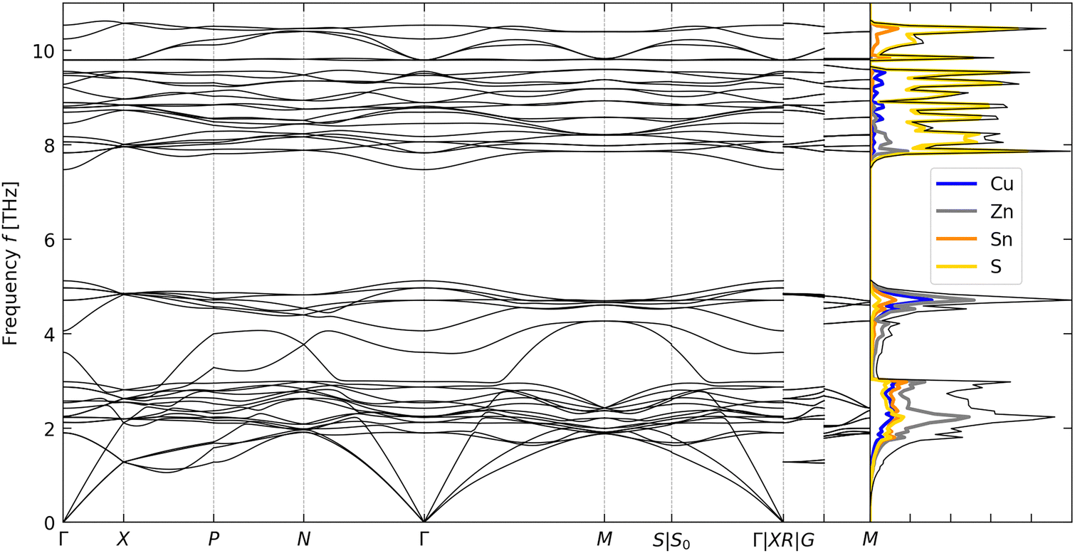 | ||
| Fig. 2 Calculated phonon dispersion and density of states (DoS) of Cu2ZnSnS4. The DoS curve shows the total DoS in black and projections onto the Cu, Zn, Sn and S atoms in blue, grey, orange and yellow, respectively. | ||
3.2 Lattice thermal conductivity
Using the single-mode relaxation-time approximation to the phonon Boltzmann equations, the lattice thermal conductivity is given by:45
 | (4) |
The macroscopic κlatt is an average over contributions κqj from individual phonon modes qj with one of Nq wavevectors q and band indices j = 1 − 3na. The size of the κqj are determined by the heat capacities Cqj, group velocities νqj and lifetimes τqj.45
We note that the κlatt is a tensor, and the three diagonal components καβ correspond to transport along the a = b (κxx = κyy) and c directions (κzz). To compare to experiments on polycrystalline films or pressed pellets with randomly-oriented crystallites, it is useful to compute the scalar average κlatt, which we denote in Roman type to distinguish it from the tensor κlatt:
 | (5) |
The computed axial καα and average κlatt are compared in Fig. 3(a). We predict thermal conductivities of 9.43 and 2.24 W m−1 K−1 at T = 300 and 1200 K, respectively, the former of which is several times larger than orthorhombic SnS (κlatt = 2.15 W m−1 K−1 at 300 K),61 Bi2S3 (0.9 W m−1 K−1)62 and Bi2SO2 (2.62 W m−1 K−1).36 In contrast to the layered (oxy)chalcogenides SnS and Bi2SO2,36,61 our calculations predict very minimal anisotropy in the κlatt of CZTS, which might be attributed to the 3D tetrahedral bonding network.
 | ||
| Fig. 3 Calculated lattice thermal conductivity καβ of Cu2ZnSnS4. Plot (a) shows the καβ as a function of temperature, while plots (b) and (c) show the harmonic function (κ/τCRTA)αβ and weighted-average lifetime τCRTAαβ defined in eqn (6) in the text. On each plot we show the principal xx = yy and zz components of the tensors, corresponding to transport along the a = b and c directions, together with the scalar averages computed using the equivalents of eqn (5). | ||
To analyse the κlatt, we used the scalar-average modal contributions κqj to compute the cumulative thermal conductivity as a function of frequency at T = 300, 600 and 900 K (Fig. S1, ESI†). At all three temperatures, approximately 80% of the κlatt is through modes with frequencies fqj ≤ 2 THz, while most of the remaining 20% is through modes with 2 < fqj ≤ 4 THz. With reference to the phonon spectrum in Fig. 2, this indicates that the majority of the transport is via the acoustic modes, with some contribution from the low-lying optic modes, and that the higher-frequency Cu/Zn- and S-based bands make a negligible contribution to the thermal transport.
To understand the origin of the high κlatt of CZTS compared to other leading chalcogenide TEs, we used the constant relaxation-time approximation (CRTA) model developed in our previous work.61,63,64 In this model, the κlatt is written as the product of a harmonic function κ/τCRTA and a weighted-average lifetime τCRTA, which are indicative of differences in the group velocities and lifetimes, respectively:
 | (6) |
We note that we have defined the τCRTA as tensors, which allows us to account for possible differences in the lifetimes of the dominant heat-carrying modes along the a = b and c axes.
The xx = yy and zz components of the κ/τCRTA and τCRTA tensors are shown together with the averages in Fig. 3(b) and (c). At T = 300 K we obtain an averaged κ/τCRTA of 0.439 W m−1 K−1 ps−1, which can be compared to values of 0.718, 0.422 and 1.46 W m−1 K−1 ps−1 for SnS, Bi2S3 and Bi2SO2.36,61,62 We have previously shown that low κ/τCRTA can be linked to inhomogeneous chemical bonding, indicators of which are large primitive cells and low-symmetry spacegroups.64 CZTS and SnS have the same-sized primitive cell (na = 8), and CZTS has a higher-symmetry spacegroup (tetragonal I vs. orthorhombic Pnma for SnS), which suggests the quaternary composition significantly reduces the group velocities. Indeed, the κ/τCRTA are comparable to Bi2S3, despite the fact that the latter has a larger, lower-symmetry primitive cell (Pnma, na = 20). On the other hand, the κ/τCRTA of Bi2SO2 are much larger, which we attribute to the smaller primitive cell (na = 5) and stronger ionic bonding.34
Our calculated average lifetime τCRTA is 21.5 ps at 300 K, which is 7–12× longer than SnSe (3 ps61), Bi2S3 (2.14 ps62) and Bi2SO2 (1.8 ps36). This more than compensates for the low group velocities and produces a large overall κlatt.
To establish the origin of the longer phonon lifetimes, we write the τqj as the product of an averaged three-phonon interaction strength ![[P with combining tilde]](https://www.rsc.org/images/entities/i_char_0050_0303.gif) and a weighted two-phonon joint density of states (w-JDoS) function N2(q,ω):45
and a weighted two-phonon joint density of states (w-JDoS) function N2(q,ω):45
 | (7) |
 | (8) |
Fig. 4(a) shows the linear fitting63,64 to obtain the at 300, 600 and 1200 K, and Fig. 4(b) shows the ![[N with combining macron]](https://www.rsc.org/images/entities/i_char_004e_0304.gif) 2 calculated at 300 K. We obtain a scaled × (3na)2 = 9.9 × 10⁻⁹ eV2, which is ∼1.5× weaker than the 2.5 × 10⁻⁸ eV2 obtained in similar calculations on SnS.61 While it is difficult to compare the w-JDoS functions quantitatively, the 2 of SnS peaks at 4.5 THz with a scaled value of 2/(3na)2 = 1.04 THz−1,61 where the equivalent scaled 2 for CZTS is around 2.5× smaller at 0.43 THz−1. Based on these differences in and 2, we would estimate CZTS to have 6× longer lifetimes, which is close to the 7× difference in the τCRTA. We can therefore attribute the longer lifetimes in CZTS compared to SnS to roughly equal contributions from weaker three-phonon interactions and a smaller scattering phase space.
2 calculated at 300 K. We obtain a scaled × (3na)2 = 9.9 × 10⁻⁹ eV2, which is ∼1.5× weaker than the 2.5 × 10⁻⁸ eV2 obtained in similar calculations on SnS.61 While it is difficult to compare the w-JDoS functions quantitatively, the 2 of SnS peaks at 4.5 THz with a scaled value of 2/(3na)2 = 1.04 THz−1,61 where the equivalent scaled 2 for CZTS is around 2.5× smaller at 0.43 THz−1. Based on these differences in and 2, we would estimate CZTS to have 6× longer lifetimes, which is close to the 7× difference in the τCRTA. We can therefore attribute the longer lifetimes in CZTS compared to SnS to roughly equal contributions from weaker three-phonon interactions and a smaller scattering phase space.
 | ||
| Fig. 4 Analysis of the phonon lifetimes in Cu2ZnSnS4 using eqn (7) in the text. (a) Scalar average lattice thermal conductivity κ as a function of the three-phonon interaction strength −1 at T = 300, 600 and 1200 K, indicating the that reproduce the calculated κ. (b) Averaged weighted two-phonon joint density of states (w-JDoS) functions (1)2 and (2)2 defined in eqn (8), calculated at T = 300 K. | ||
A likely consequence of the long phonon lifetimes are long phonon mean-free paths (MFPs) Λqj:
| Λqj = νqjτqj | (9) |
Long phonon MFPs would make the κlatt highly sensitive to the crystallite size L. The effect of finite L can be modelled by adding a boundary-scattering contribution to the phonon lifetimes given by:
 | (10) |
Fig. 5 shows the predicted κlatt as a function of crystallite size at T = 300, 600 and 1200 K. At all three temperatures, the thermal conductivity drops sharply as L is reduced from ∼1 μm to 1 nm. At 300 K, we predict a κlatt of 8.31 W m−1 K−1 for L = 1 μm, falling to 4.95, 1.59 and 0.3 W m−1 K−1 for L = 100, 10 and 1 nm. Based on these values, nanostructuring on the order of 10 nm could reduce the κlatt by ∼80%.
 | ||
| Fig. 5 Dependence of the scalar average lattice thermal conductivity κ of Cu2ZnSnS4 on the crystallite size L at T = 300, 600 and 1200 K estimated using the boundary-scattering model in eqn (10) in the text. | ||
The reported feature size of CZTS thin films is typically L < 1 μm,65–70 and the sensitivity of the κlatt to nanostructuring is clearly seen when comparing our predictions to measurements (Table 1). For example, ref. 12 reports a κlatt of ∼1 W m−1 K−1 at 700 K for CZTS nanocrystals with L ≈ 10 nm. This is well reproduced by our calculations with L = 10 nm (1.1 W m−1 K−1), and corresponds to a 72% reduction of the predicted bulk κlatt = 3.9 W m−1 K−1.
| T [K] | Crystallite or grain size L | κlatt [W m−1 K−1] | |
|---|---|---|---|
| a Determined from X-ray diffraction data.b Determined by fitting the measured κlatt to the Callaway model. | |||
| Exp.71 | 294 | 24a nm, 22.1/7.47b nm | 0.9 |
| Calc. | 300 | 5–20 nm | 1.02–2.38 |
| Calc. | 300 | 4 nm | 0.87 |
| Calc. (bulk) | 300 | — | 9.43 |
| Exp.71 | 294 | 24–28a nm, 4.25/4.54b nm | 4.0 |
| Calc. | 300 | 60 nm | 4.05 |
| Calc. | 300 | 5–30 nm | 1.02–2.94 |
| Calc. (bulk) | 300 | — | 9.43 |
| Exp.72 | 623 | 800 nm | 0.50 |
| Calc. | 620 | 800 nm | 4.06 |
| Calc. | 620 | 2–3 nm | 0.44–0.58 |
| Calc. (bulk) | 620 | — | 4.38 |
| Exp.12 | 700 | 10.6 ± 1.9 nm | 0.97 |
| Calc. | 700 | 10 nm | 1.11 |
| Calc. (bulk) | 700 | — | 3.87 |
However, there is some ambiguity in the experimentally-reported feature size, in that grains visible at longer length scales may be formed of smaller crystallites. Microscopy typically measures the grain size, whereas techniques based on X-ray diffraction or analysis of the κlatt probe the crystallite size. The interfaces between the crystallites in a larger grain would impede phonon transport, and the L in eqn (10) can thus be equated to the crystallite size. A further complication is that stacking and twinning faults are common in CZTS, and, depending on the preparation conditions, can occur with densities corresponding to nm length scales.73–75 Moreover, intrinsic defects, including e.g. vacancies and antisites, and strain promoted by small crystallites, as well as extrinsic defects introduced to optimise the charge-carrier concentration, could lead to enhanced phonon scattering and further reductions in the κlatt. All of these features could in principle have a similar effect to the interfaces between crystallites, corresponding to nm-scale L in the boundary-scattering model that are well below the measured crystallite size.
With this in mind, ref. 71 reports considerable variation in the crystallite sizes determined using X-ray diffraction (XRD) and by fitting the κlatt to the Callaway model, such that in one of the samples the Callaway model suggested an L around 5× smaller than measured by XRD. As suggested in the discussion, this likely indicates that the “effective” crystallite size for phonon transport is limited by the presence of defects. Our boundary-scattering model predicts a crystallite size of 4 nm for the as-deposited sample in this paper, which is comparable to, albeit lower than, the value obtained by fitting the κlatt. On the other hand, we predict the ∼4.5× larger κlatt obtained after sulphurization would be indicative of a 60 nm crystallite size, which is much larger than determined from both XRD measurements and from fitting the κlatt. Given the off-stoichiometry of the experimental samples, we suspect this could indicate the formation of a secondary phase with higher thermal conductivity.
Small crystallites and/or the presence of defects could explain the κlatt of 0.5 W m−1 K−1 reported for the hot-pressed powders in ref. 72. The very low thermal conductivity suggests much smaller crystallites than the reported 800 nm grains, and the L ≈ 2–3 nm estimated from the present modelling is more in keeping with results from other experimental studies.12,72
In all cases, however, the calculated κlatt for bulk CZTS is considerably larger than the measured thermal conductivities. Therefore, while the large impact of crystallite size and, potentially, of defects complicates the comparison between our predictions and experimental measurements, it is clear that the κlatt in CZTS is highly sensitive to the (effective) crystallite size, and that optimising this, through whatever means, is likely to be key to mitigating the relatively high bulk thermal conductivity compared to other (oxy-)sulphide TEs.
3.3 Electronic structure and transport properties
The calculated electronic band structure and density of states (DoS) of CZTS, obtained using the HSE06 hybrid functional, is shown in Fig. 6. The conduction band minimum (CBM) and valence band maximum (VBM) both lie at the Γ point, giving a direct bandgap of Eg = 1.28 eV. | ||
| Fig. 6 Electronic band structure and density of states (DoS) of Cu2ZnSnS4 calculated with the HSE06 hybrid functional. | ||
Experimental measurements of the bandgap range from 1.42–1.6 eV,76–78 and our predicted value thus underestimates these by 0.14–0.32 eV (10–20%; Table S2, ESI†). Our prediction is, however, very close to the measured photoluminescence peak in the experiments in ref. 79 (1.3 eV). We also note that the Eg has been reported to be highly sensitive to stoichiometry.80 Previous theoretical studies using hybrid DFT have reported values between 1.26–1.50 eV.81–85 Our values are an excellent match to the corrected GGA calculation in ref. 85, with a difference of just 2 meV (0.16%), but show a larger discrepancy of 0.22 eV (14.7%) to the HSE06 result in ref. 83. However, with Eg > 1 we would expect limited thermal generation of (intrinsic) carriers, and thus that the transport properties would be dominated by the extrinsic carriers at typical doping levels above 1018 cm−3.86–88 We therefore do not expect the underestimation of the bandgap relative to experiments to significantly impact our predictions of the transport properties.
The electrical conductivity, Seebeck coefficient and electronic thermal conductivity can be determined from the spectral conductivity Σ(ε,T) and generalised moments of the transport distribution function Ln(εF,T) given by:46
 | (11) |
 | (12) |
![[thin space (1/6-em)]](https://www.rsc.org/images/entities/char_2009.gif) 0(ε,T) is the Fermi–Dirac distribution function given by:
0(ε,T) is the Fermi–Dirac distribution function given by:
 | (13) |
| σ(εF,T) = L0(εF,T) | (14) |
 | (15) |
 | (16) |
The τkj can be computed from first-principles using electron–phonon coupling calculations. However, these are relatively expensive, and prohibitively so for complex materials with large unit cells. For semiconductors, similar accuracy can often be obtained by estimating the electron scattering rates (inverse lifetimes) within the momentum relaxation-time approximation (MRTA) using phenomenological models for the scattering matrix elements.46 In the present work, we use the expressions for the scattering rates Γkj due to acoustic deformation potential (ADP), polar-optic phonon (POP), ionised impurity (IMP) and piezoelectric (PIE) scattering defined in ref. 46. The overall τkj are then calculated by combining the four rates using Matthiessen's rule:
| τkj−1(T) = ΓADPkj(T) + ΓPOPkj(T) + ΓIMPkj(T) + ΓPIEkj(T) | (17) |
This approach has been shown to give good predictions for a variety of semiconductors,46 and has also been carefully validated against several well-studied families of TE materials including the Sn/Ge chalcogenides34,35 and the bismuth oxychalcogenides.36 We note that the parameters used in the scattering models are determined from first-principles calculations and are not, for example, inferred from similar materials or fitted from experimental measurements.
Under the assumption that doping to adjust the carrier concentration does not affect the host band structure, the εF can be adjusted to include a nominal extrinsic carrier concentration, in addition to the thermally-generated carrier populations, allowing the properties to be predicted as a function of n and T. This is termed the “rigid band approximation” (RBA). While RBA calculations can provide a useful guide for the carrier concentrations required to optimise the electrical properties,34,36,89 the approximation can break down at large n due to modulation of the electronic structure induced by heavy doping. However, to investigate this explicitly requires calculations on atomistic models with dopants, and possibly a more sophisticated treatment of the electron–phonon coupling to compute the τkj, which we consider beyond the scope of the present study.
Finally, we also note that the three electrical properties are tensors, and, as for the κlatt, the average of the three diagonal elements are most representative of pressed pellets and thin films (cf. eqn (5)). We denote these quantities in Roman type as σ, S and κel respectively.
Fig. 7 shows the predicted average σ, S, S2σ (PF) and κel for both p- and n-type CZTS with n = 1016–1022 cm−3 at a fixed T = 600 K. At this temperature, the σ is negligible up to n ≈ 1018 cm−3 for the n-type material and n ≈ 1019 cm−3 for the p-type material, after which the electrical conductivity rises substantially with n according to:
| σ(n,T) = neμ(n,T) | (18) |
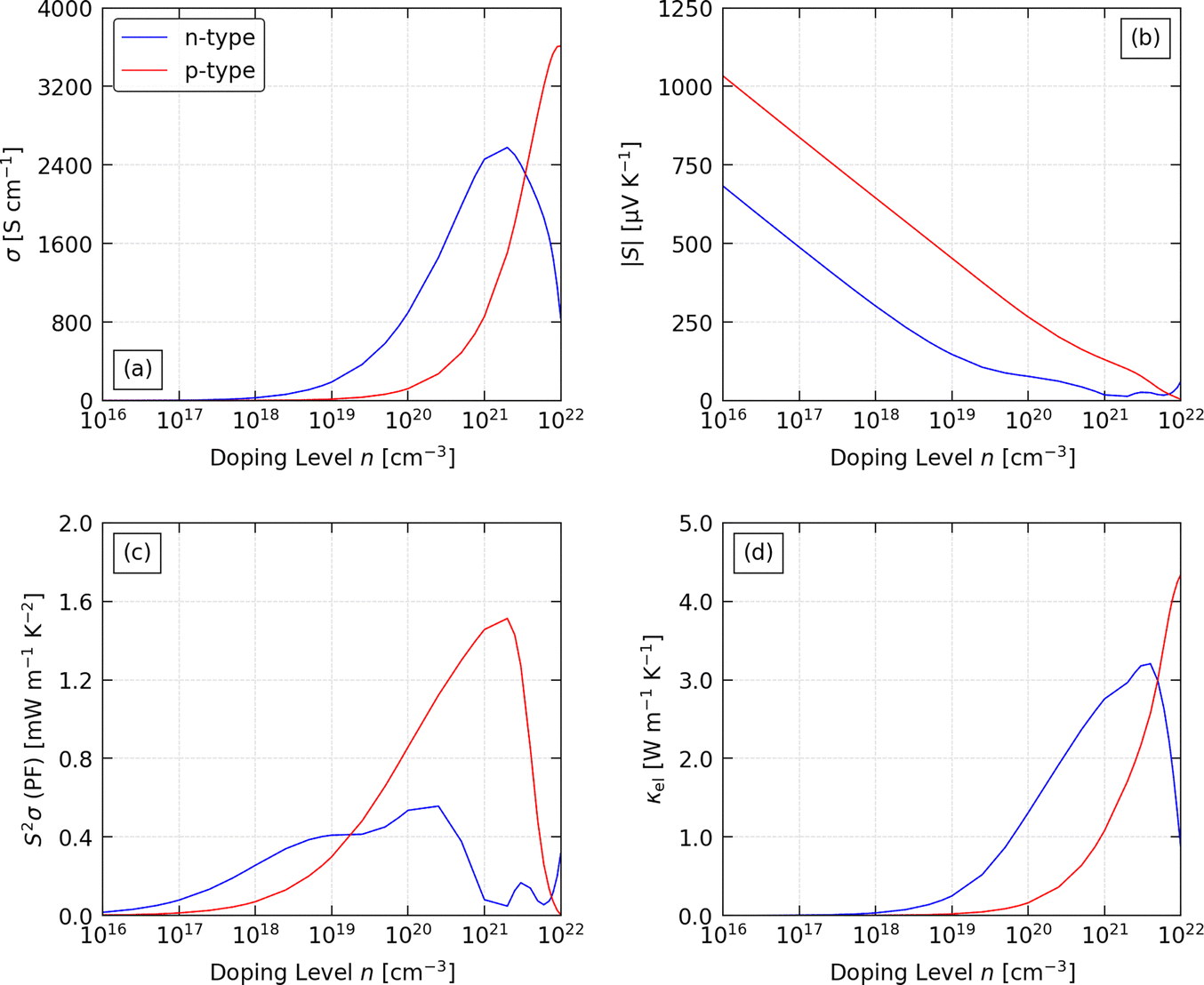 | ||
| Fig. 7 Calculated electrical properties of p- and n-type Cu2ZnSnS4 as a function of extrinsic carrier concentration n (“doping level”) at a fixed temperature T = 600 K: (a) electrical conductivity σ, (b) absolute Seebeck coefficient |S|, (c) power factor S2σ (PF), and (d) electronic thermal conductivity κel. For each property we show the scalar average values obtained using the equivalents of eqn (5) in the text. | ||
To understand this, we analysed the carrier mobilities and scattering rates from the four scattering mechanisms, and the combined (average) μ in eqn (18) (Fig. S2–S4, ESI†). For p-type doping, the μ is limited by POP scattering except at larger n → 1022 cm−3 where IMP scattering becomes competitive (Fig. S2, ESI†). The μPOP is roughly constant for n ≤ 1018 cm−3, above which it drops sharply with n. In contrast, the μPOP for n-type CZTS is an order of magnitude lower than for the p-type material at small n and remains lower up to around n ≥ 1021 cm−3 (Fig. S3, ESI†). However, IMP and PIE scattering become significant at lower n, and the higher scattering rates of all three mechanisms explain the unusual behaviour of the σ of n-type CZTS at large n (Fig. S4, ESI†).
For p-type doping, the S show an almost monotonic decrease with n, tending to zero at the largest n = 1022 cm−3 we examined. The absolute |S| with n-type doping show similar behaviour at low n, but the decrease flattens above ∼1019 cm−3, which we attribute to the unusual behaviour of the conductivity. The decrease in |S| with n is typical of the inverse relationship expected from:
 | (19) |
 is the Seebeck effective mass. The
  is related to the band effective mass
  by:90
by:90
 | (20) |
The combination of the rise in σ and decrease in |S| produces a peak in the S2σ. For p-type CZTS we obtain a relatively sharp maximum around 1021 cm−3, whereas for n-type doping we obtain a broader maximum with similar PFs from ∼1019 to 2 × 1020 cm−3. The much smaller |S| predicted for n-type CZTS results in a smaller predicted maximum PF of 0.58 mW m−1 K−2 (σ = 1218 S cm−1, S = −69 μV K−1) compared to 1.53 mW m−1 K−2 for p-type doping (σ = 1275 S cm−1, S = 110 μV K−1). We therefore predict p-type CZTS to show significantly better performance at most n, with an approximately three times higher maximum PF.
At large n the electronic thermal conductivity κel closely follows the σ according to the Wiedemann–Franz relation:
| κel(n,T) = Lσ(n,T)T | (21) |
The temperature dependence of the electrical transport properties in the degenerate regime at n = 5 × 1020 cm−3, chosen to be between the n where the maximum p- and n-type PFs are predicted to occur, is shown in Fig. S5 (ESI†). At this n, the electrical conductivity shows the metallic-like decrease with temperature expected for a degenerate semiconductor. Analysis of the temperature-dependent mobilities for the four scattering mechanisms indicates that this is primarily driven by an increase in the POP scattering rates (Fig. S6 and S7, ESI†). On the other hand, the absolute Seebeck coefficients show a significant rise with T, with a predicted 4–5× increase in the averaged |S| for both p- and n-type CZTS from 300–1000 K. For p-type CZTS, this results in a peak in the PF between 700–750 K, followed by a slow decay at higher temperature, while for the n-type material we predict a monotonic rise in the PF that levels off at higher T. The electronic thermal conductivity peaks around 400 K, which is largely due to the fall in electrical conductivity with temperature outweighing the T term in eqn (21).
In contrast to the κlatt, the σ for both p- and n-type CZTS is predicted to be strongly anisotropic (Fig. S8, ESI†), with 1.8 and 1.2× larger electrical conductivity along the a = b axes, respectively, at the n where the maximum PFs are obtained. For both doping types, there is also an almost constant offset in the |Sαβ| along the two independent directions, which becomes significant at the larger n that maximise the power factors. As a result, the maximum PFs are predicted to be 5.5× larger along the a = b direction for p-type CZTS, and 2.1× larger for n-type CZTS. These translate to modest 1.8 and 1.2× enhancement of the PFs along the a = b direction compared to the scalar averages. While this is interesting, when set against the large reductions in the κlatt we predict can be obtained by nanostructuring this finding is unlikely to be of practical use in optimising CZTS-based thermoelectric devices.
Given the large predicted effect of crystallite size on the κlatt, we performed a calculation of the electrical properties at a reference n = 5 × 1020 cm−3 and T = 600 K including a boundary-scattering term analogous to eqn (10). Fig. 8 shows the predicted PF and κel as a function of L for p- and n-type doping. Decreasing the grain size begins to impact the electrical properties from around L = 100 nm, which is 1–2 orders of magnitude lower than the L = 1–10 μm below which the κlatt starts to drop (cf. Fig. 5). This indicates that the electron MFPs are significantly shorter than the phonon MFPs. Decreasing the L from a bulk 1 mm to 1 nm reduces the p-type σ and κel by ∼50% and reduces the S by 4%. On the other hand, the n-type σ/κel are predicted to decrease to around 25% of the bulk values at L = 1 nm, but the |S| is predicted to increase by 50% from −44 μV K−1 at L = 1 mm to −65 μV K−1 at L = 1 nm. For p-type doping, reducing the L has a similar relative impact on both the PF and κel, with both falling by around 10, 20 and 50% at L = 10, 5 and 1 nm. For n-type doping, at the larger L = 5–10 nm the fall in the σ is partially offset by the increase in |S| so that the PFs are reduced by 3.5 and 11% of the bulk values, while at L = 1 nm we predict a similar 50% reduction to p-type CZTS. However, the κel is predicted to show significant decreases of ∼30, 50 and 75% at L = 10, 5 and 1 nm. Taken together with the predicted behaviour of the κlatt, this analysis suggests a crystallite size in the range of 5–10 nm is likely to yield an optimal ZT.
 | ||
| Fig. 8 Dependence of the scalar average power factor S2σ (a) and electronic thermal conductivity κel (b) of p- and n-type Cu2ZnSnS4 on the crystallite size L at n = 5 × 1020 cm−3 and T = 600 K estimated using an equivalent boundary-scattering model to eqn (10) in the text. | ||
Table 2 compares our calculated bulk electrical properties to selected experimental measurements on pristine p-type CZTS.12,86,92 Our calculations provide a relatively close match to the measurements in ref. 12, although reproducing the σ requires a 20% underestimate of the S, reproducing the S requires an order of magnitude smaller σ, and reproducing the PF requires a 1.8× larger σ and a 1.3× smaller S. There is also an order of magnitude variation in the n for the different predictions, although as the n was not measured we cannot determine which is closer to the experiments. For the other two measurements, we find the calculated n that reproduce the σ overestimate the S by a factor of 2–3×, whereas the n that reproduce the S overestimate the σ by 35–50×. Moreover, while our calculations can reproduce the measured PFs, they underestimate the σ and overestimate the S compared to the measurements. This may be because, while the calculations include a boundary-scattering model to limit the carrier mean-free paths, they do not take into account other effects that could arise in small crystallites such as carrier trapping at defects and energy filtering.93 Similarly, as alluded to during the discussion of the lattice thermal conductivity in the previous section, it is possible that strain, defects and/or dopants could impact the electrical properties in ways that cannot be reproduced by the boundary-scattering approach. These phenomena could easily account for the order-of-magnitude difference between the σ measured in the studies in ref. 86 and 92 and the values we predict based on the measured Seebeck coefficients.
| n [cm−3] | T [K] | σ [S cm−1] | S [μV K−1] | S2σ (PF) [mW m−1 K−2] | |
|---|---|---|---|---|---|
| a Grain size estimated based on electron microscopy.b Measurements compared to predictions for bulk CZTS as crystallite size has negligible impact at large L (cf. Fig. 8). | |||||
| Expt12 (10.6 ± 1.9 nm) | — | 700 | 0.37 | 990 | 3.6 × 10⁻² |
| Calc. (10 nm, best sigma) | 2.9 × 10¹⁷ | 700 | 0.35 | 783 | 2.1 × 10⁻² |
| Calc. (10 nm, best S) | 2.3 × 10¹⁶ | 700 | 0.03 | 990 | 2.8 × 10⁻³ |
| Calc. (10 nm, best PF) | 5 × 10¹⁷ | 700 | 0.69 | 724 | 3.6 × 10⁻² |
| Expt86 (32.7 nm) | 1.5 × 10¹⁸ | 573 | 1.58 | 296 | 1.4 × 10⁻² |
| Calc. (33 nm, best sigma) | 8.7 × 10¹⁷ | 573 | 1.54 | 644 | 6.4 × 10⁻² |
| Calc. (33 nm, best S) | 5.7 × 10¹⁹ | 573 | 75.7 | 298 | 0.67 |
| Calc. (33 nm, best PF) | 1.1 × 10¹⁷ | 573 | 0.2 | 819 | 1.4 × 10⁻² |
| Expt92a (2 μm) |
— | 663 | 12.4 | 170 | 3.6 × 10⁻² |
| Calc. (bulk,b best sigma) | 9.3 × 10¹⁸ | 663 | 11.7 | 482 | 0.27 |
| Calc. (bulk,b best S) | 5.3 × 10²⁰ | 663 | 458 | 173 | 1.37 |
| Calc. (bulk,b best PF) | 4.3 × 10¹⁷ | 663 | 0.64 | 738 | 3.5 × 10⁻² |
Finally, it is of interest to compare the predicted electrical properties to similar calculations on orthorhombic SnS and Bi2SO2.34–36 We previously predicted a maximum PF of 1.76 mW m−1 K−2 for p-type Pnma SnS at T = 880 K and n = 3.16 × 1019 cm−3 (σ = 226 S cm−1, S = 279 μV K−1),34,35 and a maximum PF of 0.41 mW m−1 K−2 for n-type Bi2SO2 at a higher T = 900 K and n = 5 × 1019 cm−3 (σ = 120 S cm−1, S = −186 μV K−1).36 At these temperatures, we predict that p-type CZTS can attain a maximum PF 1.58 mW m−1 K−2, which is lower than, but comparable to, p-type SnS and higher than n-type Bi2SO2.
3.4 Thermoelectric figure of merit
We now combine the calculated electrical transport properties and lattice thermal conductivity to predict the thermoelectric figure of merit ZT of p- and n-type CZTS as a function of both temperature and carrier concentration. Given that our analysis of the κlatt indicated that nanostructuring should significantly enhance the ZT, and that the majority of experiments on CZTS have focussed on thin films, we discuss here the averaged ZT calculated from the scalar average S, σ, κel and κlatt (cf. eqn (5)). Nanostructuring to crystallite sizes on the order of 10 nm appears to be readily achievable in experiments,65–70 while effective crystallite sizes below 10 nm may be accessible through e.g. defect engineering. We therefore provide predictions for bulk CZTS and for crystallite sizes of 10 and 5 nm using the boundary scattering model in eqn (10) for the κlatt and the equivalent for the S, σ and κel.Fig. 9 shows the predicted ZT as a function of n and T for bulk and nanostructured p- and n-type CZTS. In general, the largest ZT are predicted at high T and large n, due to minimising the κlatt and maximising the S2σ (cf. Fig. 6(a) and 7(c)). Both p- and n-type CZTS are predicted to show the maximum ZT, ZTmax, at the highest T = 1260 K in our calculations and at doping levels close to the n at which the peak PFs are obtained, viz. 1021 and 1020 cm−3, respectively. As expected from our analysis of the electrical transport properties, p-type CZTS is predicted to perform significantly better than n-type CZTS, with double the bulk ZTmax (0.66 vs. 0.33), but neither bulk ZTmax meets the industry requirement of ZT > 1. However, we predict that significantly larger ZTmax can be obtained by nanostructuring to reduce the large bulk κlatt. We predict that nanostructuring to 10 nm effectively doubles the p- and n-type ZTmax to 1.28 and 0.56, respectively, while further reducing the crystallite size to 5 nm will raise the ZTmax to 1.56 and 0.62.
 | ||
| Fig. 9 Predicted scalar average thermoelectric figure of merit ZT of (a), (c) and (e) p-type and (b), (d) and (f) n-type Cu2ZnSnS4 (CZTS) as a function of extrinsic carrier concentration (“doping level”) n and temperature T. Predictions are shown for (a) and (b) bulk CZTS and nanostructured CZTS with crystallite sizes of (c) and (d) L = 10 nm and (e) and (f) L = 5 nm. | ||
To better define potential application areas, Table 3 reports the predicted ZTmax attainable for p-type CZTS at 400, 600 and 1000 K, corresponding roughly to the three heat-recovery scenarios outlined in ref. 94. The predicted ZTmax = 0.22 and 0.50 at 400 and 600 K are below the industry-standard ZT > 1, whereas at 1000 K we predict that a ZTmax ≈ 1 could be achieved by nanostructuring to 10 nm, and increased by 21% to 1.15 by reducing the crystallite size to 5 nm. Data for n-type CZTS are provided in Table S3 (ESI†), and we predict ZTmax of 0.35 and 0.38 for crystallite sizes of 10 nm and 5 nm, respectively, at T = 1000 K.
| T [K] | Crystallite size L | ZTmax | n [cm−1] | σ [S cm−1] | S [μV K−1] | S2σ (PF) [mW m−1 K−2] | κ [W m−1 K−1] | ||
|---|---|---|---|---|---|---|---|---|---|
| κel | κlatt | κtot | |||||||
| 400 | Bulk | 0.06 | 2 × 10²¹ | 21.0 | 78.1 | 1.28 | 1.84 | 6.91 | 8.75 |
| 400 | 10 nm | 0.17 | 2.5 × 10²⁰ | 3.98 | 137 | 0.74 | 0.35 | 1.43 | 1.78 |
| 400 | 5 nm | 0.22 | 1020 | 1.70 | 185 | 0.59 | 0.15 | 0.93 | 1.08 |
| 600 | Bulk | 0.16 | 1021 | 8.56 | 130 | 1.46 | 1.08 | 4.53 | 5.61 |
| 600 | 10 nm | 0.40 | 2.5 × 10²⁰ | 2.49 | 201 | 1.00 | 0.32 | 1.19 | 1.52 |
| 600 | 5 nm | 0.50 | 2.5 × 10²⁰ | 2.29 | 200 | 0.91 | 0.29 | 0.81 | 1.10 |
| 1000 | Bulk | 0.45 | 7.5 × 10²⁰ | 3.73 | 199 | 1.48 | 0.57 | 2.69 | 3.27 |
| 1000 | 10 nm | 0.95 | 5 × 10²⁰ | 2.40 | 228 | 1.24 | 0.38 | 0.93 | 1.31 |
| 1000 | 5 nm | 1.15 | 5 × 10²⁰ | 2.26 | 226 | 1.16 | 0.35 | 0.65 | 1.00 |
We emphasise again that our high-temperature predictions are for pristine CZTS. The quaternary composition of CZTS can make it prone to decomposition at elevated temperature through loss of SnS and S,95–97 resulting in the formation of off-stoichiometric and secondary phases that are not accounted for in our calculations.
Our calculations yield favourable predictions of the maximum ZT between 0.025–0.039 reported in experimental studies on pristine CZTS (Table 4).12,28,98 Our predictions match the PFs, total thermal conductivity κtot and ZT reported in ref. 12 and 28 near quantitatively. On the other hand, taking the relatively large 300 nm grain size reported in ref. 98 as a crystallite size, our calculations overestimate the PF and κtot by a factor of ∼6.7×. As discussed in Section 3.2, this can likely be attributed to polycrystalline grains with a much smaller crystallite size. The relatively good predictions for the figure of merit of CZTS suggests that the discrepancies in the predicted electrical conductivity and Seebeck coefficients highlighted in the previous section to some extent compensate one another to yield reasonable PFs and ZT. While none of these three studies report carrier concentrations, we estimate n between 5 × 10¹⁷ and 3 × 1018 cm−3, and we can tentatively ascribe the low ZT to the n being much lower than we predict are required to optimise the power factor.
| n [cm−3] | T [K] | Crystallite/grain size L | S2σ (PF) [mW m−1 K−2] | κtot [W m−1 K−1] | ZT | |
|---|---|---|---|---|---|---|
| a Electrical properties calculated based on bulk CZTS as crystallite size has negligible impact at large L (cf. Fig. 8). | ||||||
| Expt (Cu2ZnSnS4)28 | — | 700 | — | 6.7 × 10⁻² | 1.21 | 3.9 × 10⁻² |
| Calc. | 1.15 × 10¹⁸ | 700 | 10 nm | 5.9 × 10⁻² | 1.11 | 3.7 × 10⁻² |
| Expt (Cu2ZnSnS4)12 | — | 700 | 10.6 ± 1.9 nm | 3.6 × 10⁻² | 0.97 | 2.5 × 10⁻² |
| Calc. | 6.6 × 10¹⁷ | 700 | 10 nm | 3.9 × 10⁻² | 1.11 | 2.5 × 10⁻² |
| Expt (Cu2ZnSnS4)98 | — | 623 | 250–300 nm | 2.1 × 10⁻² | 0.53 | 2.5 × 10⁻² |
| Calc. | 3.1 × 10¹⁸ | 623 | 300 nm + bulka | 0.14 | 3.66 | 2.4 × 10⁻² |
| Expt (Na-doped Cu2ZnSnS4)29 | — | 800 | — | 1.86 | 0.95 | 1.6 |
| Calc. | 2.3 × 10²⁰ | 800 | 1 nm | 0.60 | 0.39 | 1.22 |
| Calc. | 3 × 10²⁰ | 800 | 3 nm | 0.93 | 0.79 | 0.95 |
| Expt (Cu2(Zn,Fe,Cd)SnS4)30 | — | 550 | 1.3 μm | 0.85 | 0.68 | 0.69 |
| Calc. | 1.2 × 10²¹ | 550 | 1 μm + bulka | 1.44 | 5.91 | 0.13 |
| Calc. | 2 × 10²⁰ | 550 | 3 nm | 0.75 | 0.82 | 0.49 |
On the other hand, comparison to the Na-doped CZTS and Cu2(Zn,Fe,Cd)SnS4 solid solutions in ref. 29 and 30 is less favourable. Reproducing the ZT = 1.6 at 800 K measured in ref. 29 requires a large n = 2.3 × 1020 cm−3 and a very small crystallite size of L = 1 nm, which results in a ∼59–68% underestimate of the measured PF and κtot. Though not typical, L in the range of 2.3–7.7 nm have been reported in a number of experiments.99–103 With L = 3 nm the calculations predict a ZT of 0.95, albeit again with an underestimated PF and κtot. Similarly, to obtain a comparable figure of merit at 550 K to the ZT = 0.69 reported in ref. 30 requires much smaller crystallites than the reported grain size of 1.3 μm, and the calculations still underestimate the PF and overestimate the κtot by 11.8% and 20% respectively.
Taking these two sets of comparisons together, we are reasonably confident in our predictions for the figure of merit of pristine CZTS with modest n. However, our results suggest more in-depth modelling is needed to ascertain the effect of heavy doping to obtain larger ZT on the electronic structure and transport properties. For example, the underpredicted PF of the Cu2(Zn,Fe,Cd)SnS4 solid solutions and Na-doped CZTS could be due to the formation of resonant levels that are not captured with the rigid-band approximations.
Finally, it is also of interest to compare the predicted ZT to our previous calculations on SnS and Bi2SO2.34–36 We predicted p-type Pnma SnS to reach a maximum ZT of 1.39 at 860 K (n = 3.2 × 1019 cm−3, PF = 1.76 mW m−1 K−2, κtot = 1.09 W m−1 K−1).35 We predict that bulk p-type CZTS would have a much lower maximum ZT of 0.34 at this temperature, but that limiting the crystallite sizes to 10 and 5 nm would increase this to 0.76 and 0.92. In the latter case, we predict a PF of 1.11 mW m−1 K−2 and a κtot of 1.04 W m−1 K−1 (n = 4.04 × 1020 cm−3). Compared to SnS, CZTS has a lower power factor and a much larger intrinsic κlatt, which requires both a higher doping level and nanostructuring to offset in order to obtain a comparable ZT. On the other hand, we predicted n-type Bi2SO2 to reach a low ZT of 0.33 at 900 K (2.5 × 1019 cm−3, 0.41 mW m−1 K−2, 1.13 W m−1 K−1),36 whereas we predict n-type CZTS to show a maximum ZT of 0.27 with a crystallite size to 10 nm and n = 1.87 × 1019 cm−3 (0.38 mW m−1 K−2, 1.25 W m−1 K−1). Nanostructured CZTS could therefore potentially be competitive with Bi2SO2 as an n-type sulphide TE. We note, however, that we predicted SnS and Bi2SO2 to have potential ZT of 1.78 and 2.53, respectively, with the less widely studied n- and p-type doping, which are both far higher than we predict is achievable with CZTS.
4 Conclusions
In summary, we have used ab initio modelling to explore the thermoelectric performance of the quaternary sulphide Cu2ZnSnS4. Analysis of the lattice thermal conductivity suggests that CZTS has unusually long phonon lifetimes due to weak anharmonicity and a small scattering phase space. This results in the κlatt being highly sensitive to the crystallite size such that the bulk thermal conductivity can be reduced by >80% at the crystallite sizes of L < 10 nm reported in experiments. The calculated electrical properties indicate that p-type CZTS can support a considerably larger maximum power factor than can be obtained with electron doping, due to a higher Seebeck coefficient and a larger electrical conductivity at the n ≈ 1021 cm−3 required to optimise the p-type PF. The electrical properties are much less sensitive to the crystallite size than the κlatt, with the PFs unaffected above L ≃ 100 nm. We predict that nanostructured p-type CZTS with a crystallite size of 10 nm should yield a high-temperature ZT > 1, with the potential for improvement through further reduction in the (effective) crystallite size, although similar calculations predict that larger maximum ZT can potentially be obtained with other (oxy-)sulphide TEs. The lower maximum ZT compared to p-type SnS is partly due to the lower power factor, and so exploring the selenide analogue Cu2ZnSnSe4, or other ternary or quaternary chalcogenides with the diamondoid structure, may prove fruitful. In addition, comparison of the predicted ZT to experiments suggests that heavy doping or alloying may have the dual function of reducing the κlatt and improving the electrical transport properties beyond optimising the carrier concentration for a rigid band structure, and further computational studies to better understand these effects would also, in our view, be highly informative.Author contributions
Conceptualisation – JMS; methodology – all authors; data curation – TS and JMF; formal analysis and investigation – all authors; writing (original draft) – TS; writing (review and editing) – all authors; funding acquisition – JMS. All authors have read and agreed to the published version of the paper.Conflicts of interest
There are no conflicts to declare.Data availability
Raw data from this study will be made available to download free of charge after publication from an online repository at https://doi.org/10.17632/4d699zwynb. Our analysis code is available on GitHub at https://github.com/skelton-group/ZT-Calc-Workflow.Acknowledgements
JMS and JMF are supported by a UK Research and Innovation Future Leaders Fellowship (MR/T043121/1, MR/Y033973/1), and JMS previously held a University of Manchester Presidential Fellowship. This work used the ARCHER2 UK National Supercomputing Service via the UK Materials Chemistry Consortium (MCC; UK Engineering and Physical Sciences Research Council EP/R029431 and EP/X035859). We also made use of the UoM Computational Shared Facility (CSF), which is maintained by UoM Research IT.Notes and references
- A. Firth, B. Zhang and A. Yang, Appl. Energy, 2019, 235, 1314–1334 CrossRef.
- R. Freer and A. V. Powell, J. Mater. Chem. C, 2020, 8, 441–463 RSC.
- H. J. Goldsmid, The Seebeck and Peltier effects, Morgan & Claypool Publishers, New York, 2017, ch. 1, pp. 1-1–1-3 Search PubMed.
- C. Han, Q. Sun, Z. Li and S. X. Dou, Adv. Energy Mater., 2016, 6, 1600498 CrossRef.
- L. E. Bell, Science, 2008, 321, 1457–1461 CrossRef CAS PubMed.
- J. He and T. M. Tritt, Science, 2017, 357, eaak9997 CrossRef PubMed.
- H. Jouhara, A. Żabnieńska Góra, N. Khordehgah, Q. Doraghi, L. Ahmad, L. Norman, B. Axcell, L. Wrobel and S. Dai, Int. J. Thermofluids, 2021, 9, 100063 CrossRef CAS.
- C. Gayner and K. K. Kar, Prog. Mater. Sci., 2016, 83, 330–382 CrossRef CAS.
- Y. Liu, J. Zhi, W. Li, Q. Yang, L. Zhang and Y. Zhang, Molecules, 2023, 28, 5894 CrossRef CAS PubMed.
- G. Tan, L.-D. Zhao and M. G. Kanatzidis, Chem. Rev., 2016, 116, 12123–12149 CrossRef CAS PubMed.
- A. Kumar, S. Bano, B. Govind, A. Bhardwaj, K. Bhatt and D. K. Misra, J. Electron. Mater., 2021, 50, 6037–6059 CrossRef CAS.
- H. Yang, L. A. Jauregui, G. Zhang, Y. P. Chen and Y. Wu, Nano Lett., 2012, 12, 540–545 CrossRef CAS PubMed.
- K. Biswas, J. He, I. D. Blum, C.-I. Wu, T. P. Hogan, D. N. Seidman, V. P. Dravid and M. G. Kanatzidis, Nature, 2012, 489, 414–418 CrossRef CAS PubMed.
- Y. Lan, A. J. Minnich, G. Chen and Z. Ren, Adv. Funct. Mater., 2010, 20, 357–376 CrossRef CAS.
- T. Hendricks and W. T. Choate, Engineering Scoping Study of Thermoelectric Generator Systems for Industrial Waste Heat Recovery, 2006 Search PubMed.
- H. J. Goldsmid, Materials, 2014, 7, 2577–2592 CrossRef CAS PubMed.
- R. Freer, D. Ekren, T. Ghosh, K. Biswas, P. Qiu, S. Wan, L. Chen, S. Han, C. Fu, T. Zhu, A. K. M. A. Shawon, A. Zevalkink, K. Imasato, G. J. Snyder, M. Ozen, K. Saglik, U. Aydemir, R. Cardoso-Gil, E. Svanidze, R. Funahashi, A. V. Powell, S. Mukherjee, S. Tippireddy, P. Vaqueiro, F. Gascoin, T. Kyratsi, P. Sauerschnig and T. Mori, J. Phys.: Energy, 2022, 4, 022002 CAS.
- L.-D. Zhao, S.-H. Lo, Y. Zhang, H. Sun, G. Tan, C. Uher, C. Wolverton, V. P. Dravid and M. G. Kanatzidis, Nature, 2014, 508, 373–377 CrossRef CAS PubMed.
- L.-D. Zhao, G. Tan, S. Hao, J. He, Y. Pei, H. Chi, H. Wang, S. Gong, H. Xu, V. P. Dravid, C. Uher, G. J. Snyder, C. Wolverton and M. G. Kanatzidis, Science, 2016, 351, 141–144 CrossRef CAS PubMed.
- C. Zhou, Y. K. Lee, Y. Yu, S. Byun, Z.-Z. Luo, H. Lee, B. Ge, Y.-L. Lee, X. Chen, J. Y. Lee, O. Cojocaru-Mirédin, H. Chang, J. Im, S.-P. Cho, M. Wuttig, V. P. Dravid, M. G. Kanatzidis and I. Chung, Nat. Mater., 2021, 20, 1378–1384 CrossRef CAS PubMed.
- M. Ibáñez, R. Zamani, A. LaLonde, D. Cadavid, W. Li, A. Shavel, J. Arbiol, J. R. Morante, S. Gorsse, G. J. Snyder and A. Cabot, J. Am. Chem. Soc., 2012, 134, 4060–4063 CrossRef PubMed.
- W. G. Zeier, Y. Pei, G. Pomrehn, T. Day, N. Heinz, C. P. Heinrich, G. J. Snyder and T. Wolfgang, J. Am. Chem. Soc., 2013, 135, 726–732 CrossRef CAS PubMed.
- X. Zheng, Y. Liu, Y. Du, Y. Sun, J. Li, R. Zhang, Q. Li, P. Chen, G. Zhao, Y. Fang and N. Dai, J. Alloys Compd., 2018, 738, 484–490 CrossRef CAS.
- G. Jamwal, M. Warish, S. Muthiah, S. Chakravarty, N. Jakhar, A. Kandasami and A. Niazi, Inorg. Chem., 2022, 61, 16390–16404 CrossRef CAS PubMed.
- K. Pal, P. Singh, A. Bhaduri and K. B. Thapa, Sol. Energy Mater. Sol. Cells, 2019, 196, 138–156 CrossRef CAS.
- U. A. Shah, A. Wang, M. Irfan Ullah, M. Ishaq, I. A. Shah, Y. Zeng, M. S. Abbasi, M. A. Umair, U. Farooq, G.-X. Liang and K. Sun, Small, 2024, 20, 2310584 CrossRef CAS PubMed.
- K. Gupta, S. Gupta and Y. Batra, Mater. Sci. Eng., B, 2024, 303, 117291 CrossRef CAS.
- M.-L. Liu, I.-W. Chen, F.-Q. Huang and L.-D. Chen, Adv. Mater., 2009, 21, 3808–3812 CrossRef CAS.
- A. Nagaoka, K. Yoshino, T. Masuda, T. D. Sparks, M. A. Scarpulla and N. Kensuke, J. Mater. Chem. A, 2021, 9, 15595–15604 RSC.
- Y. Liu, P. D. McNaughter, X. Liu, A. V. Kretinin, J. M. Skelton, F. Azough, D. J. Lewis and R. Freer, ACS Appl. Mater. Interfaces, 2024, 16, 11516–11527 CrossRef CAS PubMed.
- Z. Lin, C. Hollar, J. S. Kang, A. Yin, Y. Wang, H.-Y. Shiu, Y. Huang, Y. Hu, Y. Zhang and X. Duan, Adv. Mater., 2017, 29, 1606662 CrossRef PubMed.
- C. Yang, D. Souchay, M. Kneiß, M. Bogner, H. M. Wei, M. Lorenz, O. Oeckler, G. Benstetter, Y. Q. Fu and M. Grundmann, Nat. Commun., 2017, 8, 16076 CrossRef CAS PubMed.
- R. Venkatasubramanian, E. Siivola, T. Colpitts and B. O’Quinn, Nature, 2001, 413, 597–602 CrossRef CAS PubMed.
- J. M. Flitcroft, I. Pallikara and J. M. Skelton, Solids, 2022, 3, 155–176 CrossRef CAS.
- M. Zhang, J. M. Flitcroft, S. K. Guillemot and J. M. Skelton, J. Mater. Chem. C, 2023, 11, 14833–14847 RSC.
- J. M. Flitcroft, A. Althubiani and J. M. Skelton, J. Phys.: Energy, 2024, 6, 025011 CAS.
- G. Kresse and J. Hafner, Phys. Rev. B:Condens. Matter Mater. Phys., 1993, 47, 558 CrossRef CAS PubMed.
- J. P. Perdew, A. Ruzsinszky, G. I. Csonka, O. A. Vydrov, G. E. Scuseria, L. A. Constantin, X. Zhou and K. Burke, Phys. Rev. Lett., 2008, 100, 136406 CrossRef PubMed.
- P. E. Blöchl, Phys. Rev. B:Condens. Matter Mater. Phys., 1994, 50, 17953 CrossRef PubMed.
- G. Kresse and D. Joubert, Phys. Rev. B:Condens. Matter Mater. Phys., 1999, 59, 1758 CrossRef CAS.
- H. J. Monkhorst and J. D. Pack, Phys. Rev. B, 1976, 13, 5188 CrossRef.
- A. Jain, S. P. Ong, G. Hautier, W. Chen, W. D. Richards, S. Dacek, S. Cholia, D. Gunter, D. Skinner, G. Ceder and K. A. Persson, APL Mater., 2013, 1, 011002 CrossRef.
- A. Togo, K. Shinohara and I. Tanaka, Spglib: a software library for crystal symmetry search, arXiv, 2024, preprint, arXiv:1808.01590 DOI:10.48550/arXiv.1808.01590.
- A. Togo and I. Tanaka, Scr. Mater., 2015, 108, 1–5 CrossRef CAS.
- A. Togo, L. Chaput and I. Tanaka, Phys. Rev. B:Condens. Matter Mater. Phys., 2015, 91, 094306 CrossRef.
- A. M. Ganose, J. Park, A. Faghaninia, R. Woods-Robinson, K. A. Persson and A. Jain, Nat. Commun., 2021, 12, 2222 CrossRef CAS PubMed.
- A. V. Krukau, O. A. Vydrov, A. F. Izmaylov and G. E. Scuseria, J. Chem. Phys., 2006, 125, 224106 CrossRef PubMed.
- M. Gajdoš, K. Hummer, G. Kresse, J. Furthmüller and F. Bechstedt, Phys. Rev. B:Condens. Matter Mater. Phys., 2006, 73, 045112 CrossRef.
- K. Momma and F. Izumi, J. Appl. Crystallogr., 2011, 44, 1272–1276 CrossRef CAS.
- V. Kheraj, K. K. Patel, S. J. Patel and D. V. Shah, J. Cryst. Grow., 2013, 362, 174–177 CrossRef CAS.
- T. Chandel, V. Thakur, S. Halaszova, M. Prochazka, D. Haško, D. Velic and R. Poolla, J. Electron. Mater., 2018, 47, 5477–5487 CrossRef CAS.
- J. Guo, S. Sun, B. Liu, R. Hao and L. Sun, Optik, 2021, 242, 166998 CrossRef CAS.
- M. Sahu, V. R. M. Reddy, B. Kim, B. Patro, C. Park, W. K. Kim and P. Sharma, Materials, 2022, 15, 1708 CrossRef CAS PubMed.
- N. B. M. Amiri and A. Postnikov, Phys. Rev. B:Condens. Matter Mater. Phys., 2010, 82, 205204 CrossRef.
- A. J. Jackson and A. Walsh, J. Mater. Chem. A, 2014, 2, 7829–7836 RSC.
- S. P. Ramkumar, G. Petretto, W. Chen, H. P. C. Miranda, X. Gonze and G.-M. Rignanese, Phys. Rev. Mater., 2022, 6, 035403 CrossRef CAS.
- L. Boutahar, A. Benamrani, Z. Rouabah and S. Daoud, Ann. West Univ. Timisoara, Phys., 2023, 65, 160–170 CrossRef CAS.
- J. Heyd, G. E. Scuseria and M. Ernzerhof, J. Chem. Phys., 2003, 118, 8207–8215 CrossRef CAS.
- J. M. Skelton, A. J. Jackson, M. Dimitrievska, S. K. Wallace and A. Walsh, APL Mater., 2015, 3, 041102 CrossRef.
- F. A. Cotton, G. Wilkinson, C. A. Murillio and M. Bochmann, Advanced Inorganic Chemistry, Wiley, 6th edn, 1999 Search PubMed.
- J. M. Skelton, J. Mater. Chem. C, 2021, 9, 11772–11787 RSC.
- J. Cen, I. Pallikara and J. M. Skelton, Chem. Mater., 2021, 33, 8404–8417 CrossRef CAS.
- J. Tang and J. M. Skelton, J. Phys.: Condens. Matter, 2021, 33, 164002 CrossRef CAS PubMed.
- S. K. Guillemot, A. Suwardi, N. Kaltsoyannis and J. M. Skelton, J. Mater. Chem. A, 2024, 12, 2932–2948 RSC.
- S. A. Vanalakar, G. L. Agawane, S. W. Shin, M. P. Suryawanshi, K. V. Gurav, K. S. Jeon, P. S. Patil, C. W. Jeong, J. Y. Kim and J. H. Kim, J. Alloys Compd., 2015, 619, 109–121 CrossRef CAS.
- N. Kamoun, H. Bouzouita and B. Rezig, Thin Solid Films, 2007, 515, 5949–5952 CrossRef CAS.
- M. Abusnina, M. Matin, H. R. Moutinho, J. L. Blackburn, J. Alleman, C. DeHart, B. To and M. Al-Jassim, IEEE J. Photovolt., 2015, 5, 1470–1475 Search PubMed.
- D. M. M. Alam, Chalcogenide Lett., 2014, 11, 233–239 Search PubMed.
- M. Byeon, J.-S. Bae, T.-E. Hong, E.-D. Jeong, S. Kim and Y. Kim, Korean J. Mater. Res., 2013, 23, 7–12 CAS.
- J. Zhang, B. Long, S. Cheng and W. Zhang, Int. J. Photoenergy, 2013, 2013, 1–6 Search PubMed.
- W. D. Thompson, A. Nandur and B. E. White, J. Appl. Phys., 2016, 119, 095108 CrossRef.
- S. D. Sharma, B. Khasimsaheb, Y. Y. Chen and S. Neeleshwar, Ceram. Int., 2019, 45, 2060–2068 CrossRef CAS.
- N. Kattan, B. Hou, D. J. Fermín and D. Cherns, Appl. Mater. Today, 2015, 1, 52–59 CrossRef.
- R. Ahmad, M. Brandl, M. Distaso, P. Herre, E. Spiecker, R. Hock and W. Peukert, CrystEngComm, 2015, 17, 6972–6984 RSC.
- N. Song, M. Young, F. Liu, P. Erslev, S. Wilson, S. P. Harvey, G. Teeter, Y. Huang, X. Hao and M. A. Green, Appl. Phys. Lett., 2015, 106, 252102 CrossRef.
- S. M. Pawar, B. S. Pawar, A. V. Moholkar, D. S. Choi, J. H. Yun, J. H. Moon, S. S. Kolekar and J. H. Kim, Electrochim. Acta, 2010, 55, 4057–4061 CrossRef CAS.
- H. Katagiri, K. Saitoh, T. Washio, H. Shinohara, T. Kurumadani and S. Miyajima, Sol. Energy Mater. Sol. Cells, 2001, 65, 141–148 CrossRef CAS.
- T. Chandel, V. Thakur, S. Halaszova, M. Prochazka, D. Haško, D. Velic and R. Poolla, J. Electron. Mater., 2018, 47, 5477–5487 CrossRef CAS.
- M. Altosaar, J. Raudoja, K. Timmo, M. Danilson, M. Grossberg, J. Krustok and E. Mellikov, Phys. Status Solidi A, 2008, 205, 167–170 CrossRef CAS.
- S. I. Swati, R. Matin, S. Bashar and Z. H. Mahmood, J. Phys.: Conf. Ser., 2018, 1086, 012010 CrossRef.
- J. Paier, R. Asahi, A. Nagoya and G. Kresse, Phys. Rev. B: Condens. Matter Mater. Phys., 2009, 79, 115126 CrossRef.
- C. Persson, R. Chen, H. Zhao, M. Kumar and D. Huang, Electronic Structure and Optical Properties from First-Principles Modeling, Wiley, 2014, pp. 75–105 Search PubMed.
- S. Chen, X. G. Gong, A. Walsh and S.-H. Wei, Appl. Phys. Lett., 2009, 94, 041903 CrossRef.
- C.-J. Tong, H. J. Edwards, T. D. C. Hobson, K. Durose, V. R. Dhanak, J. D. Major and K. P. McKenna, J. Phys. Chem. Lett., 2020, 11, 10463–10468 CrossRef CAS PubMed.
- M. Nishiwaki, K. Nagaya, M. Kato, S. Fujimoto, H. Tampo, T. Miyadera, M. Chikamatsu, H. Shibata and H. Fujiwara, Phys. Rev. Mater., 2018, 2, 85404 CrossRef CAS.
- K. V. Gunavathy, K. Tamilarasan, C. Rangasami and A. M. S. Arulanantham, Ceram. Int., 2020, 46, 28342–28354 CrossRef CAS.
- P. R. Ghediya, T. K. Chaudhuri and D. Vankhade, J. Alloys Compd., 2016, 685, 498–506 CrossRef CAS.
- S. Bouzida, M. Battas, E. B. Benamar, G. Schmerber, A. Dinia, M. Abd-Lefdil and M. Regragui, Mater. Res. Innovations, 2022, 26, 127–133 CrossRef CAS.
- A. Z. Khan, J. M. Flitcroft and J. M. Skelton, Mater. Adv., 2024, 5, 652–664 RSC.
- Z. M. Gibbs, F. Ricci, G. Li, H. Zhu, K. Persson, G. Ceder, G. Hautier, A. Jain and G. J. Snyder, npj Comput. Mater., 2017, 3, 8 CrossRef.
- G. S. Kumar, G. Prasad and R. O. Pohl, J. Mater. Sci., 1993, 28, 4261–4272 CrossRef CAS.
- B. D. Long, N. V. Khanh, D. N. Binh and N. H. Hai, Powder Metall., 2020, 63, 220–226 CrossRef CAS.
- D. Narducci, E. Selezneva, G. Cerofolini, S. Frabboni and G. Ottaviani, J. Solid State Chem., 2012, 193, 19–25 CrossRef CAS.
- S. LeBlanc, S. K. Yee, M. L. Scullin, C. Dames and K. E. Goodson, Renewable Sustainable Energy Rev., 2014, 32, 313–327 CrossRef CAS.
- A. Weber, R. Mainz and H. W. Schock, J. Appl. Phys., 2010, 107, 013516 CrossRef.
- A. Redinger, D. M. Berg, P. J. Dale and S. Siebentritt, J. Am. Chem. Soc., 2011, 133, 3320–3323 CrossRef CAS PubMed.
- A. J. Jackson and A. Walsh, J. Mater. Chem. A, 2014, 2, 7829–7836 RSC.
- S. D. Sharma and S. Neeleshwar, MRS Adv., 2018, 3, 1373–1378 CrossRef CAS.
- Q. Wen, Y. Li, J. Yan and C. Wang, Mater. Lett., 2015, 140, 16–19 CrossRef CAS.
- M. Boshta, S. Binetti, A. Le Donne, M. Gomaa and M. Acciarri, Mater. Technol., 2017, 32, 251–255 CrossRef.
- L. Chen and C. Park, Korean J. Chem. Eng., 2017, 34, 1187–1191 CrossRef CAS.
- S. Rondiya, A. Rokade, A. Jadhavar, S. Nair, M. Chaudhari, R. Kulkarni, A. Mayabadi, A. Funde, H. Pathan and S. Jadkar, Mater. Renewable Sustainable Energy, 2017, 6, 8 CrossRef.
- S. Y. Gezgin, A. Houimi and H. S. Kilic, Optik, 2019, 199, 163370 CrossRef CAS.
Footnote |
| † Electronic supplementary information (ESI) available: Includes comparison of the calculated lattice parameters and electronic bandgap to previous experiments and computational studies, additional data for the predicted electrical properties, and predicted maximum figures of merit and associated material parameters for n-type Cu2ZnSnS4. See DOI: https://doi.org/10.1039/d5tc01537e |
| This journal is © The Royal Society of Chemistry 2025 |