
 Open Access Article
 This Open Access Article is licensed under a
 Creative Commons Attribution 3.0 Unported Licence
Asymmetric perinone-based electron-collecting monolayer materials for n–i–p perovskite solar cells†
Julius
Petrulevicius‡
 a,
Minh Anh
Truong‡
b,
Maryte
Daskeviciene
a,
Giedre
Bubniene
a,
Shota
Hira
b,
Yasuko
Iwasaki
b,
Tadas
Malinauskas
a,
Atsushi
Wakamiya
*b and
Vytautas
Getautis
*a
a,
Minh Anh
Truong‡
b,
Maryte
Daskeviciene
a,
Giedre
Bubniene
a,
Shota
Hira
b,
Yasuko
Iwasaki
b,
Tadas
Malinauskas
a,
Atsushi
Wakamiya
*b and
Vytautas
Getautis
*a
aDepartment of Organic Chemistry, Kaunas University of Technology, Radvilenu pl. 19, Kaunas, 50254, Lithuania. E-mail: vytautas.getautis@ktu.lt
bInstitute for Chemical Research, Kyoto University, Gokasho, Uji, Kyoto 611-0011, Japan
First published on 20th June 2025
Abstract
A series of asymmetric perinone derivatives (PERNI) bearing different substituents (methyl, fluoro, chloro, bromo, and cyano) on the benzimidazole moiety were synthesized and investigated for possible application as electron-collecting monolayer materials in negative–intrinsic–positive perovskite solar cells. These compounds exhibit good thermal stability and suitable frontier molecular orbital energy levels for electron extraction and hole blocking. The perinone-based devices were found to demonstrate comparable power conversion efficiencies and higher operational stability than reference devices using the representative naphthalene diimide-based monolayer material under the same fabrication conditions. Within the PERNI series, devices fabricated with the chloro-substituted PERNI-Cl were found to tend to exhibit the highest open-circuit voltage and fill factor owing to the smallest energy offset between the lowest unoccupied molecular orbital and the conduction band of the perovskite.
Introduction
Nowadays, energy crises have raised significant concern worldwide, prompting the motivation to develop sustainable energy harvesting technologies. Photovoltaic technologies (PVs) have the potential to play a significant role in the global effort to decarbonize the energy supply by converting renewable solar energy into electricity. Perovskite solar cells (PSCs) are considered to be one of the most promising alternatives to commercial silicon-based solar cell technology. This is due to their sky-rocketing power conversion efficiencies (PCEs) and cost-effective fabrication process.1–4Most of the high-efficiency PSCs that have been reported to date are based on a solution-processed layer-by-layer stacking device structure, with a perovskite light-absorber layer sandwiched between the hole-collecting layer (HCL) and the electron-collecting layer (ECL).5 In the context of solution-processed multi-layered structures, the development of semiconducting materials exhibiting solvent resistance to the perovskite precursor solution is paramount for the charge-collecting layer situated beneath the perovskite layer (HCL for positive–intrinsic–negative (p–i–n) or ECL for n–i–p PSCs). In this regard, in the case of p–i–n PSCs, chemically adsorbed monolayer materials (or anchorable molecules) have been identified as a suitable replacement for conventional p-type metal oxide- and polymer-based hole-collecting materials (HCMs), including nickel oxide (NiOx), poly(3,4-ethylenedioxythiophene):poly(styrene sulfonate) (PEDOT:PSS), or poly[bis(4-phenyl)(2,4,6-trimethylphenyl)amine] (PTAA), etc.6 The molecular structure of monolayer materials generally consists of a π-conjugated core linked with an anchoring group (such as phosphonic acid,7–10 carboxylic acid,11–13 boronic acid,14 silane,15etc.) via an alkyl or aryl spacer. The anchoring group can chemisorb onto the surface of transparent conducting oxides (TCOs) to form a robust monolayer that can withstand the subsequent perovskite deposition. Monolayer materials have been shown to exhibit several advantages over conventional materials, including minimal parasitic absorption, low material consumption and facile molecular structure modification.16–18 Since our initial report in 2018,7 significant progress has been made in the development of hole-collecting monolayer materials,19,20 leading to significant progress in p–i–n single-3,21 and multi-junction22–27 solar cell devices.
In n–i–p PSCs, n-type metal oxides, such as titanium oxide (TiO2) and tin oxide (SnO2), are the most commonly used electron-collecting materials (ECMs). However, together with their intrinsic oxygen vacancy defects,28 the photo-catalytic activity under ultraviolet light and high-temperature sintering process (>450 °C) of TiO229 and the high batch-to-batch variation of commercial SnO2 source materials30 impede their high-throughput production. In light of the accumulated knowledge in p–i–n PSCs, organic monolayer materials are poised to emerge as promising alternatives to these conventional n-type metal oxides. However, despite recent advances in interfacial modifications that have demonstrated significant improvements in charge extraction and device stability,31 the development of monolayer material-compatible alternatives to metal oxides remains challenging. There are very few reports on electron-collecting monolayer materials for n–i–p PSCs, and these are limited to well-known fullerene,32–34 naphthalimide,35,36 and rylene diimide5,35–38 derivatives. In contrast, there are numerous efforts devoted to developing hole-collecting monolayer materials in p–i–n PSCs.39
In our research, we have focused on perinone structure as a potential electron-collecting monolayer material. Perinone (Fig. 1a), the bisbenzimidazole derivative of naphthalenetetracarboxylic anhydride, is a significant class of dyes and pigments.40,41 Furthermore, perinone derivatives have the potential to become attractive n-type semiconducting materials for organic electronic devices42–44 due to their high electron affinity.45,46 The perinone structure is known for its inherent stability, a desirable trait for ECMs in PSCs that need to withstand operational stresses like heat and prolonged light exposure, contributing to the long-term operational stability of the solar cell. Additionally, perinone derivatives can be chemically modified to fine-tune their frontier molecular orbital energy levels. Thus, achieving an optimal energy level alignment with the perovskite, facilitating efficient electron injection from the perovskite to the ECM, and minimizing energy losses.41 Most intriguingly, the π-extended version of perinone, perylene tetracarboxylic acid bisbenzimidazole (Fig. 1a), was used as an n-type semiconductor in the first heterojunction organic solar cell (OSC) developed by Tang in 1986.47 Nevertheless, perinone derivatives are less developed due to their poor solubility in organic solvents. To the best of our knowledge, there are only two reports using perinone derivatives in the field of PSCs. Song and coworkers developed a series of soluble halogen-substituted perinones (Fig. 1a) by introducing long alkyl48 or alkoxy phenyl49 groups into the naphthalene core and used them as perovskite/ECL interfacial materials in p–i–n PSCs, demonstrating promising results in terms of both efficiency and stability.
 | ||
| Fig. 1 Chemical structures of (a) perinone, its π-extended derivative, and reported soluble perinone derivatives for p–i–n PSCs, and (b) asymmetric perinone-based anchorable molecules for n–i–p PSCs in this work. | ||
In this study, we sought to address the solubility issue by designing and synthesizing a series of asymmetric perinone molecules (PERNI, Fig. 1b) capable of forming monolayers on top of the substrate. In this way, high concentrations of the material in the solution are not required. These molecules contain an imide moiety connected with a methyl phosphonic acid anchoring group on one side and a functionalized benzimidazole moiety on the other (Fig. 1). This approach was taken to mitigate the potential impact of long alkyl (or alkoxy) chains on electron transport, a concern that could hinder the efficacy of the molecules. In addition, we have thoroughly investigated the fundamental properties of these perinone derivatives, encompassing thermal, photophysical and electrochemical characteristics. Finally, we fabricated and evaluated n–i–p PSC devices using these perinone-based monolayers as electron-collecting layers.
Results and discussion
Synthesis
The synthetic route to the perinone derivatives is shown in Scheme 1, and the detailed procedures are provided in ESI.† The phosphonate ester precursor compounds (1–6) were synthesized via a one-pot synthesis protocol consisting of a condensation reaction of naphthalene-1,4,5,8-tetracarboxylic dianhydride (1.0 equiv.) and corresponding substituted o-phenylenediamine derivatives (1.0 equiv.), followed by the imidation reaction with diethyl(aminomethyl)phosphonate (1.2–1.5 equiv.). The synthesis of compounds 1–5 was carried out in dry dimethylformamide (DMF). However, it was observed that compound 6 undergoes decomposition when DMF is utilized as the reaction solvent. Consequently, for the synthesis of compound 6, DMF was replaced with glacial acetic acid. The acidic hydrolysis of the phosphonate esters 1–5 with concentrated hydrochloric acid at reflux gave the non-substituted PERNI-H (84% yield) and substituted PERNI derivatives (91, 91, 84, and 91% yield for PERNI-CH3, PERNI-F, PERNI-Cl, and PERNI-Br, respectively). In the case of cyano-substituted PERNI-CN, milder hydrolysis conditions were applied using bromo trimethylsilane at room temperature to prevent any side reactions that may occur at the –CN group. This approach resulted in the isolation of the final product, PERNI-CN, with a 57% yield. The chemical structures of the synthesized molecules were verified by means of nuclear magnetic resonance (NMR), elemental analysis, Fourier transformation infrared spectroscopy (FT-IR), and electrospray ionization (ESI) mass spectrometry.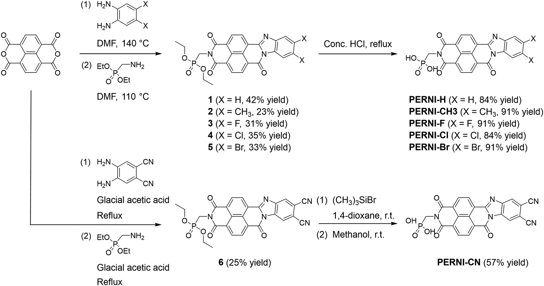 | ||
| Scheme 1 Synthesis route for asymmetric perinone-based anchorable molecules. | ||
Thermal properties
The thermal stability of the perinone derivatives was evaluated by thermogravimetric analysis (TGA). The measurements were carried out under a nitrogen atmosphere at a scan rate of 10 °C min−1. The results are displayed in Fig. 2 (see also Fig. S1 and Table S1 (ESI†) for phosphonate ester precursor compounds). The temperature corresponding to 5% weight loss (Td5) of the perinone derivatives was estimated to be in the order of PERNI-CN (228 °C) < PERNI-Cl (294 °C) < PERNI-H (326 °C) < PERNI-Br (337 °C) < PERNI-F (410 °C) < PERNI-CH3 (453 °C). The rapid weight loss exhibited by the halogen-substituted perinone derivatives, including PERNI-F, PERNI-Cl, and PERNI-Br, can be ascribed to the release of the halogen atoms. In summary, synthesized perinone derivatives exhibit adequate thermal stability for perovskite solar cell device fabrication by solution process, which is typically conducted at temperatures below 150 °C. | ||
| Fig. 2 TGA thermograms of (a) PERNI-H, PERNI-CH3, and PERNI-CN, and (b) PERNI-F, PERNI-Cl, and PERNI-Br at a scan rate of 10 °C min−1 under a nitrogen atmosphere. | ||
Theoretical calculations
In order to gain insight into the structural and electronic properties of the synthesized perinone molecules, density functional theory (DFT) calculations were performed at the B3LYP/cc-PVDZ level of theory. The side view of DFT-optimized molecular conformations (Fig. 3-bottom) demonstrates that all perinone molecules possess a rigid and planar π-conjugated framework, which is predicted to facilitate intermolecular π–π stacking in the solid state.50 | ||
| Fig. 3 Frontier Kohn–Sham molecular orbitals and the side view of the optimized molecular conformations for the perinone derivatives obtained from the theoretical calculations at the B3LYP/cc-PVDZ level of theory. | ||
As demonstrated in Fig. 3, the highest occupied molecular orbitals (HOMOs) of all molecules are distributed on the entire π-system with the exception of the imide moiety. Conversely, the lowest unoccupied molecular orbitals (LUMOs) exhibit significant delocalization over the perinone fragment. The incorporation of electron-accepting groups such as –F, –Cl, –Br, and –CN, into the benzimidazole moiety results in a decrease in the energy levels of the frontier molecular orbitals compared to the non-substituted or electron-donating group (–CH3) substituted molecule.
Photophysical properties
In order to investigate the influence of the substituted functional groups on the photophysical properties, the ultraviolet-visible (UV-vis) absorption and photoluminescence (PL) spectra of the perinone derivatives were measured in dimethylacetamide (DMA) solution. The data are presented in Fig. 4 and summarized in Table 1. All compounds exhibit two major absorption bands within the range of 300–325 nanometers (nm) and 400–455 nm, respectively. The broad and intense absorption peak in the longer wavelength region can be attributed to π → π* transitions. In comparison to non-substituted PERNI-H with exhibited a maximum absorption peak (λAbmax) observed at 433 nm, perinone derivatives with electron-accepting groups demonstrated a hypsochromic shift of 7–20 nm (λAbmax = 426, 422, 426, and 413 nm for PERNI-F, PERNI-Cl, PERNI-Br, and PERNI-CN, respectively). Conversely, a discernible bathochromic shift of 22 nm was evident in the derivative bearing the electron-donating methyl substituent (PERNI-CH3, λAbmax = 455 nm). | ||
| Fig. 4 (a) UV-vis absorption in DMA solution 10−4 M and (b) normalized photoluminescence spectra of the phosphonic acid group containing perninone derivatives. | ||
| Compound |
λ
Abmax
![[thin space (1/6-em)]](https://www.rsc.org/images/entities/char_2009.gif) [nm]
[nm] |
λ
Plmax
[nm] |
λ Stokes [nm] | λ int [nm] | E g [eV] |
|---|---|---|---|---|---|
| a Absorption spectra measured in DMA solution 10−4 M. b Photoluminescence spectra measured in DMA solution 10−5 M. c Stokes shift λStokes = λPlmax − λAbmax. d Intersection point of absorption and emission spectra in DMA solution. e Optical band gap was estimated from the intersection of absorption and emission spectra following this equation: Eg = 1240/λint. | |||||
| PERNI-H | 433 | 626 | 194 | 503 | 2.46 |
| PERNI-CH3 | 455 | 675 | 220 | 554 | 2.24 |
| PERNI-F | 426 | 604 | 178 | 484 | 2.56 |
| PERNI-Cl | 422 | 533 | 111 | 474 | 2.62 |
| PERNI-Br | 426 | 590 | 164 | 488 | 2.54 |
| PERNI-CN | 413 | 527 | 114 | 458 | 2.71 |
A similar trend was obtained for the PL spectra with the peak observed at 626, 675, 604, 533, 590, and 527 nm for PERNI-H, PERNI-CH3, PERNI-F, PERNI-Cl, PERNI-Br, and PERNI-CN, respectively. Consequently, the Stokes shift (λStokes) for these perinone derivatives was calculated to be in the range of 111–220 nm. The optical bandgap (Eg) was determined from the intersection (λint) of the absorption and photoluminescence spectra using the following equation: Eg = 1240/λint (Table 1). The experimental results align with the theoretical calculations, with the smallest and largest optical band gaps observed for PERNI-CH3 and PERNI-CN, respectively.
In comparison to the phosphonate ester precursors 1–6 (Fig. S2 and Table S2, ESI†), the PL spectra of non-substituted PERNI-H and methyl-substituted PERNI-CH3 exhibit a bathochromic shift of approximately 30 nm, while those of PERNI derivatives with electron-accepting groups, particularly chloro-substituted PERNI-Cl, demonstrate a hypsochromic shift up to 58 nm. Freshly prepared and 24 hours-aged DMA solutions of phosphonic acid-containing perinone derivatives (0.1 mM) were exposed to UV radiation (254 nm). As demonstrated in Fig. S3 (ESI†), a discernible alteration in the color of photoemission was observed for PERNI-F (from dark yellow to lime), PERNI-Cl (from gold to light green), and PERNI-Br (from orange to gold). This phenomenon indicates a shift in the emission bands towards shorter wavelengths. This phenomenon can be explained by the formation of H-type aggregates.51,52 In H-aggregates, the molecular transition dipoles are oriented “face to face”. In this configuration, the lower excited state of the two split energy levels generated by dipole interactions is optically forbidden, while the higher one is allowed.
Electrochemical properties
The electrochemical properties of the perinone derivatives were investigated by cyclic voltammetry (CV) measurements in dimethyl sulfoxide (DMSO) solution containing tetrabutylammonium hexafluorophosphate (nBu4N+PF6−, 0.1 M) and ferrocene/ferrocenium (Fc/Fc+) as the supporting electrolyte and internal standard, respectively, at a scan rate of 50 mV s−1. The cyclic voltammograms are shown in Fig. 5, and the electrochemical properties are summarized in Table 2.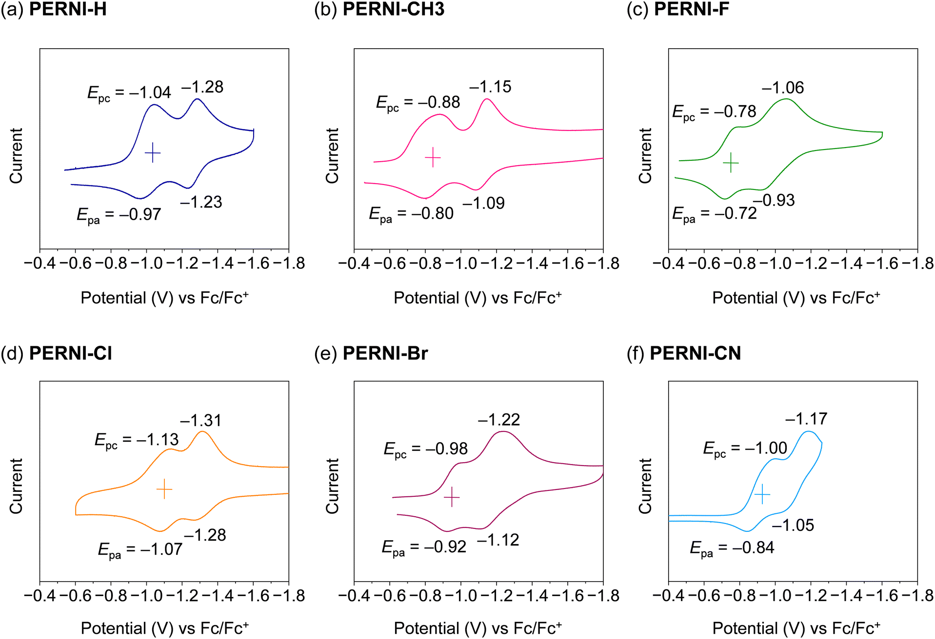 | ||
| Fig. 5 Cyclic voltammetry curves of PERNI derivatives dissolved in DMSO solution at a scan rate of 50 mV s−1. | ||
| Compound |
E
1/2redvs.Fc/Fc
+
[V] |
E LUMO [eV] | E HOMO [eV] |
|---|---|---|---|
|
a Half-wave of reduction potential E1/2red was obtained as an average value between maxima of cathodic and anodic potentials: E1/2red =1/2 × (Epc + Epa).
b Calculated from the equation ELUMO = −(5.1 + E1/2redvs.Fc/Fc+),53–55 where 5.1 eV is the vacuum energy level of ferrocene.
c Calculated from the equation EHOMO = ELUMO + Eg, Eg is the optical band gap estimated from UV-vis measurement.
|
|||
| PERNI-H | −1.01 | −4.09 | −6.55 |
| PERNI-CH3 | −0.84 | −4.26 | −6.50 |
| PERNI-F | −0.75 | −4.35 | −6.91 |
| PERNI-Cl | −1.10 | −4.00 | −6.62 |
| PERNI-Br | −0.95 | −4.15 | −6.69 |
| PERNI-CN | −0.92 | −4.18 | −6.89 |
The occurrence of quasi-reversible first reduction waves was observed for all compounds. The half-wave reduction potential (E1/2redvs. Fc/Fc+) of PERNI-H, PERNI-CH3, PERNI-F, PERNI-Cl, PERNI-Br, and PERNI-CN was estimated to be −1.01, −0.84, −0.75, −1.10, −0.95, and −0.92 V, respectively. The LUMO energy levels (ELUMO) were calculated to be −4.09, −4.26, −4.35, −4.00, −4.15, and −4.18 eV for PERNI-H, PERNI-CH3, PERNI-F, PERNI-Cl, PERNI-Br, and PERNI-CN, respectively, by using the following equation: ELUMO = −(5.1 + E1/2redvs.Fc/Fc+), where 5.1 eV is the vacuum energy level of ferrocene.53–55 Furthermore, the HOMO levels of these perinone derivatives were estimated to be in the range from −6.50 to −6.89 eV. The LUMO and HOMO levels of PERNI derivatives are found to be deeper than the conduction bands (CBs) and valence bands (VBs) of typical perovskite materials (CB = −3.90 eV and VB = −5.45 eV for MAPbI3 or CB = −3.99 eV and VB = −5.56 eV for Cs0.05FA0.80MA0.15PbI2.75Br0.25, MA: methylammonium, FA: formamidinium),56,57 indicating potential for efficient electron extraction and hole blocking from the perovskite layer.
Fabrication and evaluation of n–i–p perovskite solar cells
The present study aims to evaluate the impact of perinone derivatives as electron-collecting monolayer materials in perovskite solar cells. The n–i–p PSCs with a configuration of glass/indium tin oxide (ITO)/electron-collecting layer (ECL)/perovskite/doped 2,2′,7,7′-tetrakis-(N,N-di-4-methoxyphenylamino)-9,9′-spirobifluorene (Spiro-OMeTAD)/Au (Fig. 6a) were fabricated. For the purpose of comparison, the commercially available naphthalene diimide-based PANDI was utilized as the reference for electron-collecting monolayer materials.37 Additionally, given that the general thickness of conventional metal oxide-based ECL is ca. 40 nm,57 in this study, to mimic a monolayer condition, a very thin layer of SnO2 (ca. 3 nm) was also employed as the reference. As previously mentioned, the synthesized perinone derivatives exhibit suitable energy level matching (Fig. 6a) with our previously developed triple-cation mixed halide perovskite (Cs0.05FA0.80MA0.15PbI2.75Br0.25). For this reason, this perovskite component was selected for this study. The fabrication process for PSC devices is delineated in the ESI.† | ||
| Fig. 6 (a) Schematic structure of n–i–p PSC and energy diagram of perinone derivatives and triple-cation mixed halide perovskite used in this work. (b) and (c) J–V curves in the reverse scan of the champion devices. | ||
The morphology of the perovskite films fabricated on different perinone-based electron-collecting monolayers was evaluated by scanning electron microscopy (SEM). As demonstrated in the top-view (Fig. S4, ESI†) and cross-sectional (Fig. S5, ESI†) SEM images, irrespective of the substituents on the benzimidazole moiety, all perovskite films exhibit a smooth and pinhole-free surface. The presence of bright grains has been attributed to the presence of excess PbI2. Notably, the perovskite films fabricated on the PERNI derivatives exhibited higher coverage compared to those deposited on PANDI (Fig. S6, ESI†). This finding indicates a higher surface wettability of the PERNI-based monolayers compared to the PANDI counterpart.
The current–voltage (J–V) curves for champion devices measured under standard AM 1.5G (100 mW cm−2) illumination are shown in Fig. 6b and c. The corresponding device parameters, including short-circuit current (JSC), open-circuit voltage (VOC), fill factor (FF), and PCE, are summarized in Table 3. It is noteworthy that all devices exhibited substantial hysteresis (Table S3 and Fig. S7 and S8, ESI†), particularly in the cases of the PSCs employing electron-collecting monolayers, a finding that aligns with prior reports in the literature.34–36,58,59 Thus, we used the values derived from the reverse scan to report photovoltaic parameters.
| ECL | J SC [mA cm−2] | V OC [V] | FFa | PCEa [%] |
|---|---|---|---|---|
| a The average and standard deviation values obtained in the reverse scan from 6–18 devices were given in parentheses. | ||||
| Thin SnO2 (3 nm) | 24.1 (24.0 ± 0.1) | 0.97 (0.97 ± 0.01) | 0.67 (0.66 ± 0.01) | 15.8 (15.5 ± 0.2) |
| PANDI | 23.3 (22.9 ± 0.6) | 0.86 (0.62 ± 0.15) | 0.62 (0.53 ± 0.05) | 12.5 (7.7 ± 2.8) |
| PERNI-H | 23.1 (21.3 ± 1.4) | 0.85 (0.77 ± 0.09) | 0.59 (0.47 ± 0.11) | 11.7 (8.1 ± 3.1) |
| PERNI-CH3 | 23.4 (21.9 ± 1.4) | 0.88 (0.81 ± 0.06) | 0.61 (0.52 ± 0.09) | 12.4 (9.4 ± 2.8) |
| PERNI-F | 23.1 (22.3 ± 0.8) | 0.85 (0.81 ± 0.04) | 0.61 (0.53 ± 0.08) | 12.1 (9.8 ± 2.2) |
| PERNI-Cl | 23.0 (22.6 ± 0.5) | 0.86 (0.84 ± 0.02) | 0.63 (0.56 ± 0.07) | 12.3 (10.6 ± 1.4) |
| PERNI-Br | 23.0 (22.8 ± 0.2) | 0.85 (0.83 ± 0.02) | 0.58 (0.52 ± 0.06) | 11.4 (9.8 ± 1.1) |
| PERNI-CN | 23.3 (23.4 ± 0.7) | 0.81 (0.78 ± 0.04) | 0.62 (0.61 ± 0.02) | 11.8 (11.0 ± 0.5) |
The reference devices employing a 3 nm-thin SnO2 exhibited a maximum and average PCE of 15.8% and 15.5%, respectively. As no passivation treatment on perovskite films was utilized in the present work, the results can be regarded as comparable to those of previously reported studies.60 On the other hand, the reference devices fabricated with naphthalene diimide-based monolayer (PANDI), which has been reported as one of the most efficient electron-collecting monolayer materials to date,37 exhibited a lower maximum and average PCE of 12.5 and 7.7%, respectively. This outcome suggests that achieving comparable reproducibility from laboratory to laboratory and even batch to batch is considerably more challenging in the case of electron-collecting monolayer-based n–i–p PSCs compared to p–i–n devices with hole-collecting monolayers. From our perspective, besides intrinsic properties of electron-collecting monolayer materials, such as hydrophobicity and compatible energy levels, the impact of the transparent conducting oxide microstructure61 is also a crucial factor and should receive more studies.
Getting back to the devices using the perinone derivatives as electron-collecting monolayers. All perinone-based devices exhibited maximum and average PCEs that were comparable to those of devices employing naphthalene diimide-based PANDI (see box plots of photovoltaic parameters in Fig. S9, ESI†). The maximum (average) PCE of PERNI-H, PERNI-CH3, PERNI-F, PERNI-Cl, PERNI-Br, and PERNI-CN-based devices was estimated to be 11.7% (8.1%), 12.4% (9.4%), 12.1% (9.8%), 12.3% (10.6%), 11.4% (9.8%), and 11.8% (11.0%), respectively. The enhancement in the average PCE can be attributed to an increase in the average VOC of the perinone-based devices (0.77–0.84 V for perinone derivatives vs. 0.62 V for PANDI). Among the devices using the PERNI series, those fabricated with chloro-substituted PERNI-Cl tend to exhibit the highest VOC and FF, which is correlated with its smallest CB/LUMO energy offset (+0.01 eV for PERNI-Clvs. +0.10 to +0.36 eV for the other PERNI). The JSC values derived from the J–V curves of the perinone-based devices are in line with the integrated values estimated from the incident photon-to-current conversion efficiency (IPCE, Fig. S10, ESI†) spectra and comparable to that of the PANDI-based reference device.
The present study aims to investigate the influence of electron-collecting layers on the charge separation properties at the ECL/perovskite interface. To this end, steady-state photoluminescence (PL) quenching and time-resolved PL (TRPL) decay for the perovskite films deposited on quartz and different ITO/ECL substrates were measured. As shown in Fig. S11 and Table S4 (ESI†), after the fabrication perovskite layers on ECL substrates, the PL peak intensity was reduced to 48, 32, 14, 13, 12, 12, 11, and 4% for SnO2, PANDI, PERNI-CH3, PERNI-F, PERNI-H, PERNI-Br, PERNI-Cl, and PERNI-CN, respectively, in comparison to the pristine perovskite deposited on a quartz substrate. A double exponential function in which the fast lifetime (τ1) is associated with the charge transfer quenching at the interface, while the long lifetime (τ2) is attributed to the charge recombination quenching in the bulk, was used to fit the PL decay. The average TRPL lifetime (τave) and τ2 for the perovskite film fabricated on SnO2 were found to be 164 and 177 ns, respectively, which are longer than those of the perovskite films deposited on PANDI (τave = 74 ns, τ2 = 82 ns) and perinone derivatives (τave = 17–63 ns, τ2 = 21–68 ns). This result correlates well with the trend observed for VOC and indicates that the charge recombination in the perovskite film fabricated on SnO2 was suppressed compared to those fabricated on PANDI or PERNI derivatives, leading to higher performance of the SnO2-based devices.
The operational stability of the devices was evaluated through the implementation of maximum power point tracking (MPPT) measurement in an inert atmosphere at room temperature under AM 1.5G. It is noteworthy that the operational stability of n–i–p devices can be impacted by the incorporation of doped Spiro-OMeTAD.37 To circumvent this concern, for the MPPT measurement, a thin film of Spiro-OMeTAD was fabricated by the vacuum deposition method.56 As shown in Fig. S12 (ESI†), after 100 h, compared to the initial output, the output power of the PERNI-CN-, PERNI-Cl-, and PERNI-CH3-based devices was estimated to be 83, 73, and 60%, respectively, higher than that of the PANDI-based reference device (42%). The higher operational stability of the devices fabricated with the PERNI derivatives could be attributed to the better coverage and quality of the perovskite films on the PERNI-based monolayers compared to the case of PANDI.
Overall, as a proof-of-concept, the perinone derivatives (PERNI series) were found to be potential electron-collecting monolayer materials in n–i–p PSCs. In this work, a benzimidazole moiety has been modified with various functional groups in order to find the optimal structure. In future work, it would be beneficial to focus on modification of the naphthalene core of these molecules. Thus, finetuning the energy level alignment of the system. Additionally, we observed that the nature of the substituent at benzimidazole moiety has a significant influence on the overall device stability. Therefore, identification of even more compatible functional groups could represent a fruitful avenue for furthering this research.
Conclusions
In summary, a series of asymmetric perinone derivatives bearing different substituents (methyl, fluoro, chloro, bromo, and cyano) on the benzimidazole moiety were synthesized and investigated. These compounds are sufficiently thermally stable. Furthermore, the presence of suitable frontier molecular orbital energy levels suggests their potential to function as electron-collecting materials in n–i–p PSCs. A comparative analysis was conducted on perinone-based devices and reference devices, utilizing a naphthalene diimide-based monolayer material under identical fabrication conditions. The results indicated that both groups exhibited comparable performance. Among the synthesized perinone derivatives, devices fabricated with the chloro-substituted PERNI-Cl were found to exhibit the highest open-circuit voltage and fill factor owing to the smallest energy offset between the lowest unoccupied molecular orbital and the conduction band of the perovskite. The type of substituent at benzimidazole moiety has a marked influence on the overall device stability. We believe that obtained moderate but encouraging results and structure/properties relationships, demonstrated in this work, is another important step towards supplementing or replacing commonly employed metal oxides such as TiO2, SnO2, and ZnO as n-type electron transport layers, by adopting electron-collecting molecular monolayers in the n–i–p structure PSCs.Author contributions
The manuscript was written through contributions of all authors. All authors have given approval to the final version of the manuscript.Conflicts of interest
A. W. is co-founder and CSO of EneCoat Technologies Co., Ltd.Data availability
The data supporting this article have been included as part of the ESI.†Acknowledgements
This work was supported by International Collaborative Research Program of ICR (Kyoto University), Grant-in-Aid for Scientific Research (A) (JP24H00481), and Grant-in-Aid for Scientific Research (B) (JP24K01571). This study was in part funded by the European Union. Views and opinions expressed are however those of the author(s) only and do not necessarily reflect those of the European Union or CINEA. Neither the European Union nor the granting authority can be held responsible for them. VALHALLA project has received funding from Horizon Europe Research and Innovation Action programme under Grant Agreement no. 101082176. J. P. and T. M. acknowledge funding from the Research Council of Lithuania (LMTLT), agreement no. S-MIP-24-5. We thank Dr Richard Murdey (ICR, Kyoto University) for MPPT set up.References
- A. Kojima, K. Teshima, Y. Shirai and T. Miyasaka, J. Am. Chem. Soc., 2009, 131, 6050–6051 CrossRef CAS PubMed.
- G. Szabó, N. G. Park, F. De Angelis and P. V. Kamat, ACS Energy Lett., 2023, 8, 3829–3831 CrossRef.
- J. Du, J. Chen, B. Ouyang, A. Sun, C. Tian, R. Zhuang, C. Chen, S. Liu, Q. Chen, Z. Li, X. Wu, J. Cai, Y. Zhao, R. Li, T. Xue, T. Cen, K. Zhao and C.-C. Chen, Energy Environ. Sci., 2025, 18, 3196–3210 RSC.
- J. Zhou, L. Tan, Y. Liu, H. Li, X. Liu, M. Li, S. Wang, Y. Zhang, C. Jiang, R. Hua, W. Tress, S. Meloni and C. Yi, Joule, 2024, 8, 1691–1706 CrossRef CAS.
- W. Wang, X. Li, P. Huang, L. Yang, L. Gao, Y. Jiang, J. Hu, Y. Gao, Y. Che, J. Deng, J. Zhang and W. Tang, Adv. Mater., 2024, 36, 2407349 CrossRef CAS PubMed.
- P. Chen, Y. Xiao, S. Li, X. Jia, D. Luo, W. Zhang, H. J. Snaith, Q. Gong and R. Zhu, Chem. Rev., 2024, 124, 10623–10700 CrossRef CAS PubMed.
- A. Magomedov, A. Al-Ashouri, E. Kasparavičius, S. Strazdaite, G. Niaura, M. Jošt, T. Malinauskas, S. Albrecht and V. Getautis, Adv. Energy Mater., 2018, 8, 1801892 CrossRef.
- M. A. Truong, T. Funasaki, L. Ueberricke, W. Nojo, R. Murdey, T. Yamada, S. Hu, A. Akatsuka, N. Sekiguchi, S. Hira, L. Xie, T. Nakamura, N. Shioya, D. Kan, Y. Tsuji, S. Iikubo, H. Yoshida, Y. Shimakawa, T. Hasegawa, Y. Kanemitsu, T. Suzuki and A. Wakamiya, J. Am. Chem. Soc., 2023, 145, 7528–7539 CrossRef CAS PubMed.
- A. Al-Ashouri, A. Magomedov, M. Roß, M. Jošt, M. Talaikis, G. Chistiakova, T. Bertram, J. A. Márquez, E. Köhnen, E. Kasparavičius, S. Levcenco, L. Gil-Escrig, C. J. Hages, R. Schlatmann, B. Rech, T. Malinauskas, T. Unold, C. A. Kaufmann, L. Korte, G. Niaura, V. Getautis and S. Albrecht, Energy Environ. Sci., 2019, 12, 3356–3369 RSC.
- M. A. Truong, L. Ueberricke, T. Funasaki, Y. Adachi, S. Hira, S. Hu, T. Yamada, N. Sekiguchi, T. Nakamura, R. Murdey, S. Iikubo, Y. Kanemitsu and A. Wakamiya, Angew. Chem., Int. Ed., 2024, 63, e202412939 CrossRef CAS PubMed.
- E. Yalcin, M. Can, C. Rodriguez-Seco, E. Aktas, R. Pudi, W. Cambarau, S. Demic and E. Palomares, Energy Environ. Sci., 2019, 12, 230–237 RSC.
- M. A. Truong, T. Funasaki, Y. Adachi, S. Hira, T. Tan, A. Akatsuka, T. Yamada, Y. Iwasaki, Y. Matsushige, R. Kaneko, C. Asahara, T. Nakamura, R. Murdey, H. Yoshida, Y. Kanemitsu and A. Wakamiya, J. Am. Chem. Soc., 2025, 147, 2797–2808 CrossRef CAS PubMed.
- E. Aktas, N. Phung, H. Köbler, D. A. González, M. Méndez, I. Kafedjiska, S. H. Turren-Cruz, R. Wenisch, I. Lauermann, A. Abate and E. Palomares, Energy Environ. Sci., 2021, 14, 3976–3985 RSC.
- H. Guo, C. Liu, H. Hu, S. Zhang, X. Ji, X.-M. Cao, Z. Ning, W.-H. Zhu, H. Tian and Y. Wu, Natl. Sci. Rev., 2023, 10, nwad057 CrossRef CAS PubMed.
- H. Tang, Z. Shen, Y. Shen, G. Yan, Y. Wang, Q. Han and L. Han, Science, 2024, 383, 1236–1240 CrossRef CAS PubMed.
- M. Li, M. Liu, F. Qi, F. R. Lin and A. K. Y. Jen, Chem. Rev., 2024, 124, 2138–2204 CrossRef CAS PubMed.
- Y. Yao, C. Cheng, C. Zhang, H. Hu, K. Wang and S. De Wolf, Adv. Mater., 2022, 34, 2203794 CrossRef CAS PubMed.
- F. H. Isikgor, S. Zhumagali, L. V. Luis, M. De Bastiani, I. McCulloch and S. De Wolf, Nat. Rev. Mater., 2023, 8, 89–108 CrossRef CAS.
- C. E. Puerto Galvis, D. A. González Ruiz, E. Martínez-Ferrero and E. Palomares, Chem. Sci., 2023, 15, 1534–1556 RSC.
- C. Li, Y. Chen, Z. Zhang, C. Liu, F. Guo, W. Ahmad and P. Gao, Energy Environ. Sci., 2024, 17, 6157–6203 RSC.
- K. Zhao, Q. Liu, L. Yao, C. Değer, J. Shen, X. Zhang, P. Shi, Y. Tian, Y. Luo, J. Xu, J. Zhou, D. Jin, S. Wang, W. Fan, S. Zhang, S. Chu, X. Wang, L. Tian, R. Liu, L. Zhang, I. Yavuz, H. Wang, D. Yang, R. Wang and J. Xue, Nature, 2024, 632, 301–306 CrossRef CAS PubMed.
- Z. Liu, R. Lin, M. Wei, M. Yin, P. Wu, M. Li, L. Li, Y. Wang, G. Chen, V. Carnevali, L. Agosta, V. Slama, N. Lempesis, Z. Wang, M. Wang, Y. Deng, H. Luo, H. Gao, U. Rothlisberger, S. M. Zakeeruddin, X. Luo, Y. Liu, M. Grätzel and H. Tan, Nat. Mater., 2025, 24, 252–259 CrossRef CAS PubMed.
- S. Hu, J. Wang, P. Zhao, J. Pascual, J. Wang, F. Rombach, A. Dasgupta, W. Liu, M. A. Truong, H. Zhu, M. Kober-Czerny, J. N. Drysdale, J. A. Smith, Z. Yuan, G. J. W. Aalbers, N. R. M. Schipper, J. Yao, K. Nakano, H. Turren-Cruz, J. M. Ball, D. P. Mcmeekin, K.-A. Zaininger, Z. Liu, N. K. Noel, K. Tajima, W. Chen, M. Ehara, R. A. J. Janssen, A. Wakamiya and H. J. Snaith, Nature, 2025, 639, 93–101 CrossRef CAS PubMed.
- S. Mariotti, E. Köhnen, F. Scheler, K. Sveinbjörnsson, L. Zimmermann, M. Piot, F. Yang, B. Li, J. Warby, A. Musiienko, D. Menzel, F. Lang, S. Keßler, I. Levine, D. Mantione, A. Al-Ashouri, M. S. Härtel, K. Xu, A. Cruz, J. Kurpiers, P. Wagner, H. Köbler, J. Li, A. Magomedov, D. Mecerreyes, E. Unger, A. Abate, M. Stolterfoht, B. Stannowski, R. Schlatmann, L. Korte and S. Albrecht, Science, 2023, 381, 63–69 CrossRef CAS PubMed.
- X. Y. Chin, D. Turkay, J. A. Steele, S. Tabean, S. Eswara, M. Mensi, P. Fiala, C. M. Wolff, A. Paracchino, K. Artuk, D. Jacobs, Q. Guesnay, F. Sahli, G. Andreatta, M. Boccard, Q. Jeangros and C. Ballif, Science, 2023, 381, 59–63 CrossRef CAS PubMed.
- M. Jošt, E. Köhnen, A. Al-Ashouri, T. Bertram, Š. Tomšič, A. Magomedov, E. Kasparavicius, T. Kodalle, B. Lipovšek, V. Getautis, R. Schlatmann, C. A. Kaufmann, S. Albrecht and M. Topič, ACS Energy Lett., 2022, 7, 1298–1307 CrossRef.
- X. Jiang, S. Qin, L. Meng, G. He, J. Zhang, Y. Wang, Y. Zhu, T. Zou, Y. Gong, Z. Chen, G. Sun, M. Liu, X. Li, F. Lang and Y. Li, Nature, 2024, 635, 860–866 CrossRef PubMed.
- W. Hui, X. Kang, B. Wang, D. Li, Z. Su, Y. Bao, L. Gu, B. Zhang, X. Gao, L. Song and W. Huang, Nano Lett., 2023, 23, 2195–2202 CrossRef CAS PubMed.
- N. Fan, Y. Wang, C. Zhang, G. Zhu, G. Du, K. Wei, J. Deng, Z. Luo, L. Yang and J. Zhang, J. Mater. Chem. A, 2022, 10, 8911–8922 RSC.
- J. Deng, X. Huang, Y. Che, X. Wang, X. Zhang, B. Wu, L. Yang and J. Zhang, Adv. Funct. Mater., 2024, 34, 2408392 CrossRef CAS.
- K. Li, Y. Zhu, X. Chang, M. Zhou, X. Yu, X. Zhao, T. Wang, Z. Cai, X. Zhu, H. Wang, J. Chen and T. Zhu, Adv. Energy Mater., 2025, 15, 2404335 CrossRef CAS.
- Y. C. Wang, X. Li, L. Zhu, X. Liu, W. Zhang and J. Fang, Adv. Energy Mater., 2017, 7, 1701144 CrossRef.
- Y. Hou, X. Du, S. Scheiner, D. P. McMeekin, Z. Wang, N. Li, M. S. Killian, H. Chen, M. Richter, I. Levchuk, N. Schrenker, E. Spiecker, T. Stubhan, N. A. Luechinger, A. Hirsch, P. Schmuki, H. P. Steinrück, R. H. Fink, M. Halik, H. J. Snaith and C. J. Brabec, Science, 2017, 358, 1192–1197 CrossRef CAS PubMed.
- P. Topolovsek, F. Lamberti, T. Gatti, A. Cito, J. M. Ball, E. Menna, C. Gadermaier and A. Petrozza, J. Mater. Chem. A, 2017, 5, 11882–11893 RSC.
- L. Li, Y. Wu, E. Li, C. Shen, H. Zhang, X. Xu, G. Wu, M. Cai and W. H. Zhu, Chem. Commun., 2019, 55, 13239–13242 RSC.
- S. O. Fürer, K. J. Rietwyk, F. Pulvirenti, D. P. McMeekin, M. A. Surmiak, S. R. Raga, W. Mao, X. Lin, Y. Hora, J. Wang, Y. Shi, S. Barlow, D. S. Ginger, S. R. Marder and U. Bach, ACS Appl. Energy Mater., 2023, 6, 667–677 CrossRef.
- D. S. Utomo, L. M. Svirskaite, A. Prasetio, V. Malinauskiene, P. Dally, E. Aydin, A. Musiienko, V. Getautis, T. Malinauskas, R. Azmi and S. De Wolf, ACS Energy Lett., 2024, 9, 1682–1692 CrossRef CAS.
- F. Ye, D. Zhang, X. Xu, H. Guo, S. Liu, S. Zhang, Y. Wu and W. H. Zhu, Sol. RRL, 2021, 5, 2000736 CrossRef CAS.
- X. Chen, Z. Yue, H. Yang, B. Xu and Y. Cheng, Small, 2025, 21, 2411312 CrossRef CAS PubMed.
- J. Mizuguchi, J. Phys. Chem. B, 2004, 108, 8926–8930 CrossRef CAS.
- M. Łapkowski, Materials, 2021, 14, 6880 CrossRef PubMed.
- M. Mamada, C. Pérez-Bolívar and P. Anzenbacher, Org. Lett., 2011, 13, 4882–4885 CrossRef CAS PubMed.
- M. Mamada, C. Pérez-Bolívar, D. Kumaki, N. A. Esipenko, S. Tokito and P. Anzenbacher, Chem. – Eur. J., 2014, 20, 11835–11846 CrossRef CAS PubMed.
- R. P. Ortiz, H. Herrera, R. Blanco, H. Huang, A. Facchetti, T. J. Marks, Y. Zheng and J. L. Segura, J. Am. Chem. Soc., 2010, 132, 8440–8452 CrossRef CAS PubMed.
- E. H. Menke, V. Lami, Y. Vaynzof and M. Mastalerz, Chem. Commun., 2016, 52, 1048–1051 RSC.
- E. H. Menke, D. Leibold, A. P. Ullrich, Y. Vaynzof and M. Mastalerz, Org. Chem. Front., 2017, 4, 834–838 RSC.
- C. W. Tang, Appl. Phys. Lett., 1986, 48, 183–185 CrossRef CAS.
- X. Zhang, T. Xu, Z. Tian, X. He, S. Zhang, L. Ai, W. Zhang, S. Liu and W. Song, Chem. Commun., 2023, 59, 5874–5877 RSC.
- S. Zhang, T. Xu, P. Wu, J. Pan, W. Zhang and W. Song, J. Mater. Chem. C, 2024, 12, 4676–4681 RSC.
- T. Okamoto, S. Kumagai, E. Fukuzaki, H. Ishii, G. Watanabe, N. Niitsu, T. Annaka, M. Yamagishi, Y. Tani, H. Sugiura, T. Watanabe, S. Watanabe and J. Takeya, Sci. Adv., 2020, 6, eaaz0632 CrossRef CAS PubMed.
- N. R. Ávila-Rovelo and A. Ruiz-Carretero, Org. Mater., 2020, 2, 47–63 CrossRef.
- S. Ma, S. Du, G. Pan, S. Dai, B. Xu and W. Tian, Aggregate, 2021, 2, e96 CrossRef CAS.
- C. M. Cardona, W. Li, A. E. Kaifer, D. Stockdale and G. C. Bazan, Adv. Mater., 2011, 23, 2367–2371 CrossRef CAS PubMed.
- W. Senevirathna, J. Y. Liao, Z. Mao, J. Gu, M. Porter, C. Wang, R. Fernando and G. Sauvé, J. Mater. Chem. A, 2015, 3, 4203–4214 RSC.
- E. Misselwitz, J. Spengler, F. Rominger and M. Kivala, Chem. Commun., 2025, 61, 5754–5757 RSC.
- M. A. Truong, H. Lee, A. Shimazaki, R. Mishima, M. Hino, K. Yamamoto, K. Otsuka, T. Handa, Y. Kanemitsu, R. Murdey and A. Wakamiya, ACS Appl. Energy Mater., 2021, 4, 1484–1495 CrossRef CAS.
- S. Daskeviciute-Geguziene, M. A. Truong, K. Rakstys, M. Daskeviciene, R. Hashimoto, R. Murdey, T. Yamada, Y. Kanemitsu, V. Jankauskas, A. Wakamiya and V. Getautis, ACS Appl. Mater. Interfaces, 2024, 16, 1206–1216 CrossRef CAS PubMed.
- Y. Miyake, T. Nakamura, M. A. Truong, R. Murdey and A. Wakamiya, Chem. - Asian J., 2025, 20, e202401344 CrossRef CAS PubMed.
- K. Wojciechowski, S. D. Stranks, A. Abate, G. Sadoughi, A. Sadhanala, N. Kopidakis, G. Rumbles, C. Z. Li, R. H. Friend, A. K.-Y. Jen and H. J. Snaith, ACS Nano, 2014, 8, 12701–12709 CrossRef CAS PubMed.
- W. S. Suh, G. H. Park, S. H. Jung, Y. N. Lee, H. S. Kim, J. H. Pan and W. I. Lee, Sustainable Energy Fuels, 2024, 8, 5214–5224 RSC.
- S. Kralj, P. Dally, P. Bampoulis, B. Vishal, S. De Wolf and M. Morales-Masis, ACS Mater. Lett., 2024, 6, 366–374 CrossRef CAS PubMed.
Footnotes |
| † Electronic supplementary information (ESI) available. See DOI: https://doi.org/10.1039/d5tc01485a |
| ‡ J. P. and M. A. T. contributed equally to this work. |
| This journal is © The Royal Society of Chemistry 2025 |