
Pure red emitting elastic organic single crystals as flexible optical waveguides and circuits†
Bhargav Jyoti Bora ,
M. R. Keerthanaa and
Mari Annadhasan*
,
M. R. Keerthanaa and
Mari Annadhasan*
Department of Chemistry, Indian Institute of Technology Hyderabad, Kandi, Sangareddy, Telangana-502285, India. E-mail: annadhasan@chy.iith.ac.in
First published on 27th June 2025
Abstract
The crystal engineering approach has been advanced to precisely tune organic crystals' mechanical and optical properties and expand their potential as prospective materials in optoelectronic devices. However, the bottleneck for full-color emissive devices is that they require pure-color emissive materials. Herein, we achieved the design of a flexible single crystal of N-(3-bromo-5-chlorosalicylidene)-1-aminopyrene (ACBS), which not only exhibits excellent elastic flexibility but also shows the rare property of pure red emission with the standard Commission Internationale de l’Eclairage (CIE) coordinates of (0.67, 0.33). The single crystal structure revealed characteristic herringbone chains, which impart them with remarkable elasticity. Notably, realizing their unique standard red emissions, we show the first example of a flexible organic optical waveguide comprising a pyrene unit. The crystals were shown to be capable of propagating their fluorescence effectively, thus exhibiting potential as an active waveguide. A reconfigurable 2 × 2 directional coupler (DC) was also designed to demonstrate circuits for integrated photonic devices. This study broadens the scope for achieving all-organic flexible crystalline materials with saturated red emissions for flexible photonic, optoelectronic, and full-color devices.
Introduction
Organic crystalline materials have emerged as an essential class of solid-state materials in the field of nanophotonics owing to their superior optical properties with high photoluminescence quantum yield (PLYQ), easy synthesis and processability, lightweight nature, and ease of probing the structure–property relationship.1,2 With the advent of modern-day optoelectronic and photonic devices, the realization that organic crystals, traditionally considered brittle, can be engineered to showcase mechanical flexibility has boosted research in this field over the last decade.3–10 Exploring mechanically compliant elastic organic crystals (EOCs) with optical properties is one of the key targets in today's cutting-edge research for applications in flexible devices.11,12 The pioneer contribution given by Reddy and Ghosh, where they showed reversible elastic bending in caffeine co-crystals, marked the onset of realizing more such flexible organic single crystals.4 Such elastic mechanical properties have been primarily attributed to corrugated structures with isotropic packing arrangements, capable of dissipating strain in all directions without irreversible deformations, thereby acting as structural buffers.13–15Despite the extensive research towards developing EOCs, the underlying structural origins for their flexibility still cannot be generalized.16–18 Thus, the effect of macroscopic shape changes on the microscopic structural variations upon applying mechanical perturbations needs to be clarified. Hence, in addition to probing mechanistic subtleties in the deformed state at the bulk scale by analyzing their crystal packing,19–22 gaining a deeper understanding of short-range atomistic-scale structural variations during such deformations is a challenging task that requires more sophisticated material design. Quantifying bulk mechanical properties with micro-scale perturbations through nanoindentation techniques23,24 aided by atomic-scale analysis using micro-focus infrared (micro-IR), Raman, and X-ray diffraction18,25–27 proved to be revolutionary for improving our knowledge and gaining newer insights into the bending process. This, in turn, can have implications for the rational design of luminescent flexible EOCs with desired optical and mechanical properties, which were previously often discovered only serendipitously.
In the exploration of designing flexible organic crystals, much focus has been given to developing π-conjugated molecules capable of displaying optimal fluorescent properties for optical applications.28,29 Such mechanically soft luminescent crystals actively contribute towards the design of optical waveguides (OWGs) with high optical performance for fabricating next-generation telecommunication and integrated photonic devices.30–32 However, achieving deep-red or near-infrared flexible crystalline emitters required for practical applications remains a challenge, as most OWGs reported so far were mainly found to emit in the range of 400–600 nm. Zhang and co-workers showed excellent elastic bending ability with red emissions, and reported excellent waveguiding performances both at the straight and bent state.33,34 Chandrasekar et al. showcased the effective use of atomic force microscopy for the micromanipulation of flexible microcrystals to spatially control and guide the light.32,35 Progressively, with mechanophotonics coming into play, the construction of photonic components like bent waveguides, directional couplers, and ring resonators for miniaturized photonic devices took a new leap from the traditional approach towards device fabrication.36–38 As most commercially available optical waveguides work in the longer wavelength region of the spectrum, these works signify the importance of such flexible crystals in fabricating modern-day miniaturized photonic/optoelectronic devices.
Pyrene-based luminogens have seldom been explored for waveguiding applications, wherein the pyrene core capable of showing π-stacking interactions could induce long wavelength emissions.39,40 A few pyrene-based Schiff base compounds have been reported with a focus on exploring their elasticity41,42 and optical properties.43,44 However, to our knowledge, their applications as potential flexible optical waveguides have yet to be explored. These types of molecules, with their relatively planar donor-acceptor structure and extensive π-conjugation, show excellent luminescence properties, and their π-stacking ability helps improve their mechanical compliance as well as charge-carrier mobility for waveguiding applications. Furthermore, it is noteworthy that while there are fewer reports of organic optical waveguides exhibiting deep-red emissions, those demonstrating pure red emissions with color purity are even more rare34 and challenging to achieve. Thus, our work seeks to address this gap. Moreover, the present work is focused on pyrene-based Schiff bases and their applications for flexible optical waveguides and photonic integrated circuits. Herein, we report an elastically flexible crystal, N-(3-bromo-5-chlorosalicylidene)-1-aminopyrene (ACBS), which shows intense red emission in the crystalline state. The design strategy was such that the extensive π-conjugation with donor-acceptor moieties would promote long-wavelength emissions. At the same time, the halogens in the molecular structure would facilitate weak intermolecular interactions to bring about mechanical compliance in the crystals. Notably, the elastic crystals showed saturated red emissions with Commission Internationale de L’Eclairage (CIE) coordinates of (0.67, 0.33), which fall in the standard range for pure red color. One-dimensional single crystals of ACBS show excellent photophysical, mechanical, and optical waveguiding propensities. Also, we extended the application to create 2D photonic integrated circuits by designing and showcasing a 2 × 2 directional coupler (DC) using these elastically bending flexible crystals.
Results and discussion
The model compound was synthesized by the liquid-assisted grinding (LAG) method, where an equimolar ratio of the starting materials was taken and ground in a mortar and pestle while dropping 30 μL of methanol at regular intervals (Fig. 1a). The formation of ACBS was evident from the visible color change from pale yellow to orange, as depicted in the photographs (Fig. 1b). The reaction mixture shows a red shift in its emission color from green to intense red, and its color turns orange-red upon grinding for 10 min. The resulting product was purified and characterized by 1H, 13C NMR, and IR spectroscopy (Fig. S1–S3, ESI†). The disappearance of the characteristic –C![[double bond, length as m-dash]](https://www.rsc.org/images/entities/char_e001.gif) O peaks and red-shifted imine peaks confirmed the formation of the desired model compound. The UV-vis absorption of ACBS extends to the visible region of the spectrum (250–650 nm), and the emission spectra cover 550–800 nm with a λmax at 633 nm, with the absolute fluorescence (FL) quantum yield (Φf) of 9.52% and a lifetime of 0.84 ns (Fig. 2 and Fig. S4, ESI†). The broadband absorption and red-shifted emission of the ACBS crystals can be attributed to the increased conjugation and intermolecular π-stacking of the pyrene core.45 Remarkably, they were found to exhibit saturated red emissions as displayed in the CIE coordinates (0.67, 0.33), owing to the narrow emission curve, with a full width at half maximum (FWHM) of about 70 nm.46 Under UV light irradiation, ACBS crystals exhibit brighter fluorescence at their tips, revealing their optical waveguiding or light transducing properties (Fig. 2b).
O peaks and red-shifted imine peaks confirmed the formation of the desired model compound. The UV-vis absorption of ACBS extends to the visible region of the spectrum (250–650 nm), and the emission spectra cover 550–800 nm with a λmax at 633 nm, with the absolute fluorescence (FL) quantum yield (Φf) of 9.52% and a lifetime of 0.84 ns (Fig. 2 and Fig. S4, ESI†). The broadband absorption and red-shifted emission of the ACBS crystals can be attributed to the increased conjugation and intermolecular π-stacking of the pyrene core.45 Remarkably, they were found to exhibit saturated red emissions as displayed in the CIE coordinates (0.67, 0.33), owing to the narrow emission curve, with a full width at half maximum (FWHM) of about 70 nm.46 Under UV light irradiation, ACBS crystals exhibit brighter fluorescence at their tips, revealing their optical waveguiding or light transducing properties (Fig. 2b).
 | ||
| Fig. 1 (a) Synthetic scheme for the compound ACBS. (b) Photographs of the LAG synthesis of ACBS taken at different time intervals under ambient light (top) and UV light (bottom); all scale bars are set to 2 cm. | ||
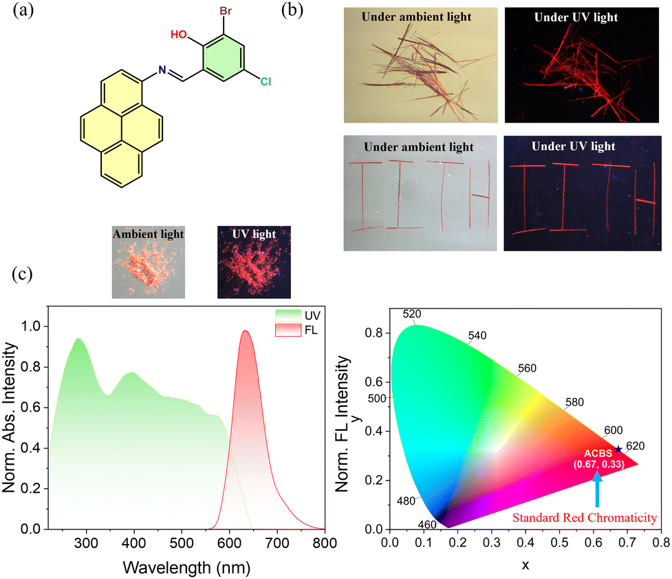 | ||
| Fig. 2 (a) Molecular structure of ACBS. (b) Photographs of the crystals under ambient and UV light. (c) Normalized UV-vis absorption and emission spectra in the solid state (insets show the photograph of the powder sample under ambient and UV light), and the corresponding CIE plot displaying the coordinates of the resulting emission. | ||
The sample was then directly crystallized by dissolving in DCM.
Subsequently, toluene and ethanol were slowly diffused along the walls of the test tube in a 2![[thin space (1/6-em)]](https://www.rsc.org/images/entities/char_2009.gif) :1:0.5 ratio, ensuring separate layers were formed. Red-colored, long acicular crystals were formed after a few days. Single crystal X-ray diffraction (SCXRD) data were collected for a straight crystal to gain information regarding the various interactions and their packing structures. ACBS crystallized in a monoclinic crystal system (P21/n space group) with two molecules in the asymmetric unit in a head–tail fashion (for detailed cell parameters, see ESI,† Table S1). Evidently, the simulated PXRD pattern generated from the single-crystal XRD data was comparable to the experimental pattern of the bulk ACBS crystals, thus indicating their phase purity (Fig. S5, ESI†). Each molecule is assisted by strong intramolecular hydrogen bonds (–N⋯H distance (in Å): 1.750) between –CHN (imine group) and the OH (hydroxyl group), and thus exists as a nearly planar structure between the pyrene and the benzene moieties with a low torsion angle of 2.94° (Fig. 3). These nearly planar molecules adopt a trans conformation across the –CHN bond. As expected, intermolecular π–π stacking interactions (3.390 Å) between the electron-rich pyrene units of one ACBS molecule and the anti-parallel electron-deficient benzene unit of an adjacent ACBS molecule are formed (Fig. 3b), thus providing a densely packed layered structure through such weak van der Waals interactions. These dimers form extended (ACBS⋯ACBS) (ACBS⋯ACBS) continuous columns along the bc plane (Fig. 3c). These columns are connected via CH⋯HC (H⋯H, 2.376 Å) and C–H⋯C (H⋯C, 2.828 Å) weak interactions in the ac plane. Additionally, the dimers are connected through multiple non-covalent interactions, such as C–H⋯Cl (H⋯Cl, 2.944 Å), C–Br⋯C (Br⋯C, 3.546 Å), and C–H⋯π (H⋯C, 2.881 Å, 2.829 Å), running along the ab plane and adopting a herringbone-type packing that grows along the crystallographic a axis. These crisscross packing patterns with periodic arrays of weak interactions in mutually perpendicular directions form an essential prerequisite, while manifesting elastic properties in crystals. Notably, while performing such studies, the single crystals were observed to be mechanically soft on the major face and bending under the force of the needle. Hence, we subjected the crystals to simple mechanical stress to qualitatively examine this flexibility. Upon applying external stress perpendicular to its longest axis with the three-point bending method through a pair of forceps and a needle (see schematic representation, Fig. 4a), the crystals show elastic bending property. Further bending forms a half-loop without breaking/cracking, as shown in the microscopic images (Fig. 4b–g and Fig. S6, ESI†). Also, a single crystal could be bent into multiple loops, as shown in Fig. 4k, to give an ‘S’ shape, displaying its excellent flexible nature. To inspect any damage to the crystals on account of such bending events, field-emission scanning electron microscopy (FESEM) images were taken of the crystals manipulated to form such an ‘S’ shape and a half-loop, which revealed no cracks or damage in the bent region, and the crystal maintained its smooth morphology (Fig. 4l and Fig. S7, ESI†). On releasing the external force, the crystals immediately returned to their original shape, revealing their excellent elastic flexibility (see Video S1, ESI†). The reproducibility of its deformation was tested by performing repeated bending-relaxing cycles (50 times each) at four different displacements (bending angles), i.e., 0.73 mm (121°) and 0.76 mm (114°), and 0.61 mm (60°) and 0.55 mm (70°), along the +y and −y-axis, without any visible fracture. The crystal remains intact before and after the bending cycles (the first 15 cycles at higher bending angles are shown in Video S2, ESI†), as shown in the red dotted boxes (Fig. 4m and Video S2, ESI†), showcasing its strong restorative power even for higher bending angles. However, when the crystals were bent above their threshold limit, they fragmented into two pieces, each retaining its elastic bending ability. Moreover, the broken pieces showed no plastic deformation even after crossing their elastic limit, indicating their sole elastic behavior. To gain in-depth mechanistic insight into the elastic bending process, we further analyzed their packing structures and interactions, which could provide a microscopic correlation of the intermolecular interactions with their macroscopic mechanical properties. Face indexing and BFDH morphology revealed (−101/10−1) to be the major face (Fig. S8, ESI†) that grows along the crystallographic short axis (b axis) by forming strong columns through π-stacking with other ACBS molecules (as discussed). The molecular packing is viewed down the bendable minor (00−1/001) face (Fig. 3d) running along the b-axis. Upon mechanical stress down the major face (−101), the π–π separation within the interconnected network of molecular chains is expected to change, thus dissipating the local strain created. The molecules pack in herringbone chains parallel to the crystallographic a axis, forming extended zigzag tapes comprising weak C–H⋯π, C–H⋯Cl, and C–Br⋯C interactions between the stacked molecules to give a crisscross arrangement. These weak interactions can act as structural buffers (blue region, Fig. 3d) that are necessary to impart elasticity in a crystal during the bending process,4,5 acting like a spring. So, when the external stress is applied, the long-range movement of the molecules is restricted by such zigzag patterns, thereby preventing slippage of the molecular layers, as seen in cases of plastic deformation. The magnified view of the herringbone stacks (Fig. 3d) clearly shows the different weak and dispersive interactions present in the buffer region (blue-shaded), which essentially are able to contain the strain generated locally as they are prone to rupture and reform in response to the loading and unloading of stress. In these herringbone stacks, the molecules are inclined to each other at a corrugation angle of ≈52° between the two adjacent stacks. Consequently, this corrugation angle changes during a bending cycle due to the presence of a multitude of dispersive interactions in the active buffer regions as part of well-established mechanisms in such elastic crystals.47 As is well-known in an elastic crystal, the π–π interaction distance can also simultaneously increase to expand the outer arc and decrease to compress the inner arc during bending through the rotation and movement of molecules from their equilibrium position.8,18 As the energy barrier for such collective movement is minimal, this helps the crystal to release the strain uniformly in the outer arc. In contrast, the inner arc undergoes greater corrugation as opposed to the middle neutral layer, where the separation distance between the molecules remains constant (Fig. 5a). All of the short-range coordinated movements of the molecules, along with the subsequent restoring ability of these interactions, enhance the dynamic characteristics of the crystal and can impart elasticity that is similar to that of a spring. However, just as a spring, if the external stress exceeds a certain threshold limit of the crystal, it disrupts the entire packing structure and leads to its breaking, as also observed under the microscope.
:1:0.5 ratio, ensuring separate layers were formed. Red-colored, long acicular crystals were formed after a few days. Single crystal X-ray diffraction (SCXRD) data were collected for a straight crystal to gain information regarding the various interactions and their packing structures. ACBS crystallized in a monoclinic crystal system (P21/n space group) with two molecules in the asymmetric unit in a head–tail fashion (for detailed cell parameters, see ESI,† Table S1). Evidently, the simulated PXRD pattern generated from the single-crystal XRD data was comparable to the experimental pattern of the bulk ACBS crystals, thus indicating their phase purity (Fig. S5, ESI†). Each molecule is assisted by strong intramolecular hydrogen bonds (–N⋯H distance (in Å): 1.750) between –CHN (imine group) and the OH (hydroxyl group), and thus exists as a nearly planar structure between the pyrene and the benzene moieties with a low torsion angle of 2.94° (Fig. 3). These nearly planar molecules adopt a trans conformation across the –CHN bond. As expected, intermolecular π–π stacking interactions (3.390 Å) between the electron-rich pyrene units of one ACBS molecule and the anti-parallel electron-deficient benzene unit of an adjacent ACBS molecule are formed (Fig. 3b), thus providing a densely packed layered structure through such weak van der Waals interactions. These dimers form extended (ACBS⋯ACBS) (ACBS⋯ACBS) continuous columns along the bc plane (Fig. 3c). These columns are connected via CH⋯HC (H⋯H, 2.376 Å) and C–H⋯C (H⋯C, 2.828 Å) weak interactions in the ac plane. Additionally, the dimers are connected through multiple non-covalent interactions, such as C–H⋯Cl (H⋯Cl, 2.944 Å), C–Br⋯C (Br⋯C, 3.546 Å), and C–H⋯π (H⋯C, 2.881 Å, 2.829 Å), running along the ab plane and adopting a herringbone-type packing that grows along the crystallographic a axis. These crisscross packing patterns with periodic arrays of weak interactions in mutually perpendicular directions form an essential prerequisite, while manifesting elastic properties in crystals. Notably, while performing such studies, the single crystals were observed to be mechanically soft on the major face and bending under the force of the needle. Hence, we subjected the crystals to simple mechanical stress to qualitatively examine this flexibility. Upon applying external stress perpendicular to its longest axis with the three-point bending method through a pair of forceps and a needle (see schematic representation, Fig. 4a), the crystals show elastic bending property. Further bending forms a half-loop without breaking/cracking, as shown in the microscopic images (Fig. 4b–g and Fig. S6, ESI†). Also, a single crystal could be bent into multiple loops, as shown in Fig. 4k, to give an ‘S’ shape, displaying its excellent flexible nature. To inspect any damage to the crystals on account of such bending events, field-emission scanning electron microscopy (FESEM) images were taken of the crystals manipulated to form such an ‘S’ shape and a half-loop, which revealed no cracks or damage in the bent region, and the crystal maintained its smooth morphology (Fig. 4l and Fig. S7, ESI†). On releasing the external force, the crystals immediately returned to their original shape, revealing their excellent elastic flexibility (see Video S1, ESI†). The reproducibility of its deformation was tested by performing repeated bending-relaxing cycles (50 times each) at four different displacements (bending angles), i.e., 0.73 mm (121°) and 0.76 mm (114°), and 0.61 mm (60°) and 0.55 mm (70°), along the +y and −y-axis, without any visible fracture. The crystal remains intact before and after the bending cycles (the first 15 cycles at higher bending angles are shown in Video S2, ESI†), as shown in the red dotted boxes (Fig. 4m and Video S2, ESI†), showcasing its strong restorative power even for higher bending angles. However, when the crystals were bent above their threshold limit, they fragmented into two pieces, each retaining its elastic bending ability. Moreover, the broken pieces showed no plastic deformation even after crossing their elastic limit, indicating their sole elastic behavior. To gain in-depth mechanistic insight into the elastic bending process, we further analyzed their packing structures and interactions, which could provide a microscopic correlation of the intermolecular interactions with their macroscopic mechanical properties. Face indexing and BFDH morphology revealed (−101/10−1) to be the major face (Fig. S8, ESI†) that grows along the crystallographic short axis (b axis) by forming strong columns through π-stacking with other ACBS molecules (as discussed). The molecular packing is viewed down the bendable minor (00−1/001) face (Fig. 3d) running along the b-axis. Upon mechanical stress down the major face (−101), the π–π separation within the interconnected network of molecular chains is expected to change, thus dissipating the local strain created. The molecules pack in herringbone chains parallel to the crystallographic a axis, forming extended zigzag tapes comprising weak C–H⋯π, C–H⋯Cl, and C–Br⋯C interactions between the stacked molecules to give a crisscross arrangement. These weak interactions can act as structural buffers (blue region, Fig. 3d) that are necessary to impart elasticity in a crystal during the bending process,4,5 acting like a spring. So, when the external stress is applied, the long-range movement of the molecules is restricted by such zigzag patterns, thereby preventing slippage of the molecular layers, as seen in cases of plastic deformation. The magnified view of the herringbone stacks (Fig. 3d) clearly shows the different weak and dispersive interactions present in the buffer region (blue-shaded), which essentially are able to contain the strain generated locally as they are prone to rupture and reform in response to the loading and unloading of stress. In these herringbone stacks, the molecules are inclined to each other at a corrugation angle of ≈52° between the two adjacent stacks. Consequently, this corrugation angle changes during a bending cycle due to the presence of a multitude of dispersive interactions in the active buffer regions as part of well-established mechanisms in such elastic crystals.47 As is well-known in an elastic crystal, the π–π interaction distance can also simultaneously increase to expand the outer arc and decrease to compress the inner arc during bending through the rotation and movement of molecules from their equilibrium position.8,18 As the energy barrier for such collective movement is minimal, this helps the crystal to release the strain uniformly in the outer arc. In contrast, the inner arc undergoes greater corrugation as opposed to the middle neutral layer, where the separation distance between the molecules remains constant (Fig. 5a). All of the short-range coordinated movements of the molecules, along with the subsequent restoring ability of these interactions, enhance the dynamic characteristics of the crystal and can impart elasticity that is similar to that of a spring. However, just as a spring, if the external stress exceeds a certain threshold limit of the crystal, it disrupts the entire packing structure and leads to its breaking, as also observed under the microscope.
 | ||
| Fig. 3 SCXRD structure of ACBS. (a) Top view, (b) side view, and (c) crystal packing of ACBS dimers and the interconnected networks (different interactions are shown in color-coded dotted lines, as depicted below), and (d) crystal morphology and packing as viewed down the (−101), (00−1) and (011) faces (the green and blue shades represent π–π stacking interactions and the presence of the buffer region, respectively). | ||
 | ||
| Fig. 4 (a) Schematic of the three-point bending of a single crystal of ACBS. (b)–(i) Elastic bending of the ACBS crystal along the major crystal face and its recovery. (j) Images displaying the bending of a single crystal to various degrees upon manipulation by a needle. (k) Multiple bending instances of a crystal to form an ‘S’ shape. (l) FESEM images of a crystal with a double bend and the corresponding close-up views of the labeled red dotted boxes (1, 2) shown at the bottom. (m) Bending at different angles and the graphs representing the bending cycles (small errors in the displacement cycles were omitted for clarity). Scale bars are set to 0.2 mm. | ||
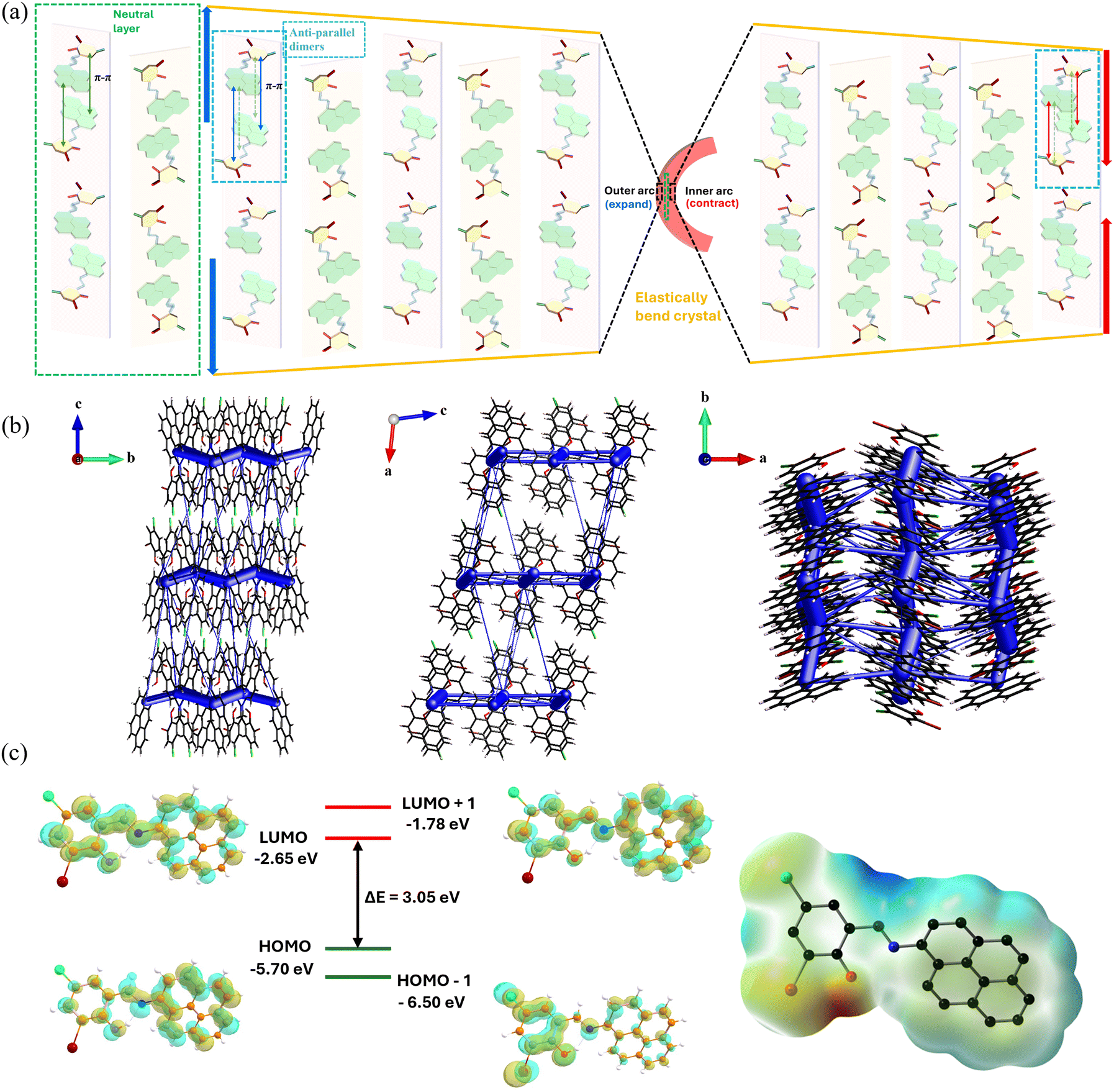 | ||
| Fig. 5 (a) Schematic depicting the possible mechanism of elastic bending with changes in the π–π distance between a pair of anti-parallel dimers. (b) Energy framework depicting the total interaction energy (blue cylinders) along the three crystallographic directions. (c) Frontier molecular orbitals (isovalue = 0.02) of ACBS and its colored electrostatic potential surface (ESP). | ||
We have also carried out energy framework calculations (Fig. S9, ESI†) to provide a theoretical basis for the elastic bending capability of the ACBS crystal, wherein the intermolecular interaction energies were computed, and the topologies along different crystallographic directions were analyzed. As displayed, the size of the cylinders is proportional to the magnitude of the interaction energies between the molecular pairs joined by their centre of mass. It is evident from the intermolecular interaction topology that the π–π interactions running along the needle axis of the crystal constitute the dominant energy, as visualized by the thick cylinders. The molecular columns form strong interactions between the herringbone stacking along the b-axis (−95.8 kJ mol−1). During the bending cycle, local variation in the π-stacked columns via adjustment and redistribution of these π–π interaction energies across the bend facilitates the deformation by accommodating the stress. As shown in Fig. 5b, the total interaction energy constituted by C–H⋯Cl and C–Br⋯C interactions along the other two directions is relatively weaker (<−10 kJ mol−1), which can evidently be broken and reformed to sustain the generated strain. Their energy framework reveals interlocked and essentially isotropic interaction energies, serving as the active buffer regions to dissipate the strain energy during bending, which is a crucial prerequisite that is generally observed for elastic bendable crystals. The interaction isotropy can also be seen in the Coulomb and dispersion energies, as denoted separately in Fig. S10, ESI,† evidencing the isotropic packing in the ACBS crystals. Furthermore, to investigate and understand the observed optical properties of our model compound, we performed ground-state structural optimization with density functional theory (DFT) calculations. The energy calculations were carried out using time-dependent DFT (TD-DFT) for the excited state and estimated vertical electron transitions to rationalize the absorption properties, and to corroborate the photophysical properties of our model compound. The frontier molecular orbitals, i.e., the HOMO and LUMO were observed to be predominantly localized over the entire molecule, with a band gap of approximately 3.05 eV (Fig. 5c). Although the HOMO shows that both the pyrene core and the benzene unit comprise most of the electron density, the contribution from the benzene ring is less as compared to the pyrene core. The LUMO, however, indicates a shift in the electron density towards the benzene unit. The TD-DFT calculations revealed a longer wavelength and a lower energy absorption band centered at 453 nm corresponding to a HOMO–LUMO transition, which can be assigned to S0 → S1, with the highest oscillatory frequency of f = 0.566 (Fig. S11 and Table S2, ESI†). The absorption maximum and the two high absorption bands with f = 0.147 and f = 0.106 can be assigned as an admixture of n, π*, and π–π* transitions. The electrostatic potential surface (ESP) of the displayed ACBS (Fig. 5c) reveals the overall charge distribution present in the molecule, where the most negative potential (red color), positive potential (blue color), and neutral potential (green and yellow) can be visualized.
Complementing the above qualitative studies, to gain a quantitative insight into the observed mechanical properties, we performed nanoindentation experiments on the major face (−101) plane of the crystals to quantify their elastic nature (Fig. 6a). The load–displacement (P–h) curves were obtained by performing the indentations perpendicular to the major face using a three-sided pyramidal Berkovich tip (total included angle of 142.30°), wherein the applied loads (P) of 4 mN and 2 mN and the corresponding penetration depths (h) were monitored continuously to obtain the elastic modulus (E) and hardness (H) of the ACBS crystal. Analyzing the P–h curve upon indenting the major face, we observed higher depth recovery upon unloading, thus denoting the mechanically soft nature of this bendable face (Fig. 6b and Fig. S12, ESI†). Notably, no pop-in phenomenon was observed in the curve for 4 mN, which suggests that there was no occurrence of local elastic-to-plastic transitions and a smooth penetration of the indenter's tip into the crystal surface during loading. However, a few pop-in events were observed for the 2 mN load. This may be due to the intermittent and localized plastic deformations that occur at such a lower load, while at a higher load, the material starts to deform more uniformly.48 The derived E and H values of the indented face deduced from the P–h curve at 4 and 2 mN force are 9.86 ± 0.37 GPa and 0.25 ± 0.05 GPa, and 8.19 ± 0.22 GPa and 0.25 ± 0.02 GPa, respectively, which are consistent and fall within the range of previously reported values of elastic organic soft crystals.49 The scanning probe images during indentation further confirmed the absence of any fracture around the indenter impression, suggesting its elastic recovery upon unloading. Thus, these results collectively indicate the elastically soft nature of the bendable major face of the ACBS crystals. Furthermore, the elastic strain on a single crystal of ACBS was calculated by applying force on the above-determined soft face by bending through different degrees to form a half-loop to achieve high strain values, as depicted in Fig. 6f, further underscoring its remarkable elastic properties. In an effort to replicate such bending behavior, we took crystals with varying lengths and widths and demonstrated their potential to achieve controlled bending, as shown in Fig. S13, ESI.† All of the calculated elastic strains reflect the range of bending degrees that can be achieved without causing any fracture, as also supported by the FESEM images (Fig. 4 and Fig. S7, ESI†), reinforcing its potential for flexible applications.
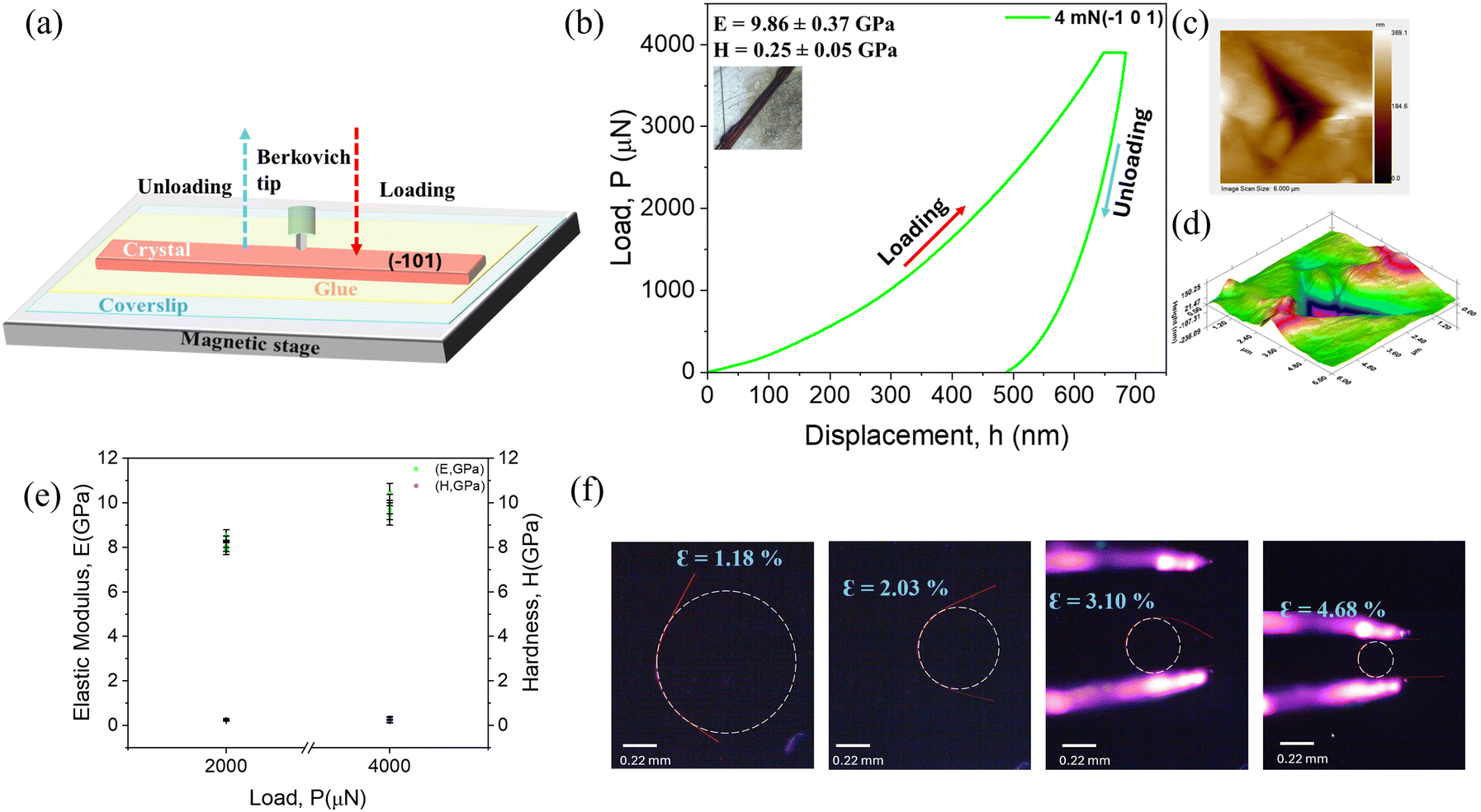 | ||
| Fig. 6 (a) Schematic setup of the nanoindentation experiment with the axis of the tip approaching perpendicular to the (−101) face of the crystal. (b) Load–displacement (P–h) curve obtained by the indenter; inset shows a crystal upon which the indents were done. (c) 2D image of the indenter impression on the crystal surface, and (d) its corresponding 3D map. (e) Corresponding error bars showing the standard deviations in the E and H values. (f) Images under UV light showing increasing strain values of a crystal during bending. | ||
Thermal stability is an important factor contributing to real-world device applications. To evaluate the stability of our compound at higher temperatures, we performed a thermal analysis of the crystals. A single endothermic peak was observed, which shows the formation of a single phase with a high melting point of 206 °C (Fig. S14, ESI†). The TGA curve depicts its stability with increasing temperatures, as there is no weight loss even after crossing its melting point, and its decomposition starts after 300 °C (Fig. S15, ESI†). Their high thermal resistance can be associated with strong intramolecular hydrogen bonds within the molecular framework.
The single crystals of ACBS, with their good optical and thermal properties and high PLQY (Φf), showed bright emissions at the tip of their terminals upon irradiation with a UV light (Fig. 2b), demonstrating their potential as a red emissive optical waveguide. As modern-day photonic devices mandate the integration of flexible waveguides,50 its waveguiding potential was evaluated both in the straight and bent forms. Initially, we took a long straight microcrystal (Fig. S16b, ESI†) and cut it at two points (end 1 and end 2, Fig. S16c and d, ESI†) with the AFM cantilever tip. The fragmented piece was pushed away from the targeted crystal (white box, Fig. S16c and d, ESI†), which bent elastically and adhered to the surface, exhibiting the pseudo-plastic nature of the microcrystal. Upon exciting one of its tips with a 532 nm laser source, the straight microcrystal, L ≈ 220 μm (shown at the top of Fig. S16a, ESI†), propagated its own FL emission to the other end of the crystal, thus behaving as an active waveguide. Thereby, we excited the crystal at different positions (148, 126.5, 101, 61, and 22 μm) and observed the emission at the tips of the crystal. As shown in Fig. S16a (ESI†), the emission intensity at the other end of the crystal gradually decreases as the distance between the tip and irradiated position increases due to an increase in propagation loss, common in flexible waveguides.30–33 The targeted straight microcrystal was then bent by gradually applying force simultaneously to its left and right sides (Fig. S16f–k, ESI†) to form an arc (facing down), as shown at the top of Fig. S16n (ESI†). The spectra collected by irradiating the bent microcrystal showed an emission maximum at 612 nm with a shoulder peak around 655 nm, which could be due to the reabsorption of its own FL (Fig. 2c). To compare the effect of bending on its waveguiding nature, we also excited a bent waveguide at different positions. We readily observed optical output at both tips of the crystal, which indicates that the crystal quality (without defects) was preserved after manipulation with the AFM cantilever tip. The bent crystal was excited through a range of distances (≈190, 169, 156, 123, and 95 μm), and the optical output was observed at the other end for each case (Fig. S16o, ESI†). Similarly, another microcrystal (in its close vicinity) was bent in an opposite direction (Fig. S16l, ESI†) and an arc could be formed facing up (see Video S3, ESI†), showcasing their excellent flexibilities and the ability to micromanipulate these crystals effectively to desired arcs. Furthermore, to quantify the waveguiding performance, we measured the distance-dependent spectra wherein we excited a straight crystal (L ≈ 529 μm) at different positions (L ≈ 529, 471, 409, 349, 286, 225, 159, 99, 50 and 0 μm), and recorded the emission spectra at the right tip of the crystal (collection terminal). As shown in Fig. 7, the emission intensity at the right tip of the crystal gradually decreases as the distance between the tip and the irradiated position increases due to an increase in the propagation loss. By fitting the data into the decay function, Itip/Ibody = exp(−αD), the optical loss coefficient (OLC) was calculated to be α′ = 0.0427 dB μm−1, demonstrating its quite good active waveguiding property. Similarly, the optical waveguiding property of the bent crystal (L ≈ 417 μm) was measured at different excitation distances (417, 377, 335, 289, 246, 194, 130, 88, 48 and 0 μm) and its OLC (α′) was calculated to be 0.0607 dB μm−1, comparable to the unbent crystal OLC. This clearly shows the minimal effect of the bent curvature on transmission loss. These results show the potential of ACBS microcrystals as elastically flexible and red-emitting active waveguides to be incorporated and used to fabricate miniaturized photonic devices by mechanical manipulation of such microwaveguides.
 | ||
| Fig. 7 (a) Optical waveguiding study. Confocal bright field (top) and FL images of the (a) straight and (b) bent microcrystals excited by a 532 nm laser at different positions. (c) and (d) Emission spectra of the straight and bent microcrystals, respectively, at different excitation positions (broken arrows showing the direction of light propagation), and (e) plot of Itip/Ibody vs. the propagation distance showing the exponential decay. | ||
For the fabrication of photonic devices, it is rational to showcase the potential of such crystals to build and design circuits capable of guiding and propagating the light in different directions. The ability to control and direct the light path through flexible waveguides enhances the versatility of such devices. To illustrate this capability, we have designed and displayed the utility of these crystals in constructing circuits by forming a 2 × 2 DC (Fig. 8), which could split and propagate the input light in a controlled manner. We took two mm-size single crystals of ACBS (thickness ≈ 1.78 and 2.35 μm), manipulated them with a needle to form the curved geometry as shown, and integrated them together to form a monolithic DC while ensuring physical contact between them at the junction, as clearly revealed by the FESEM images (Fig. 8b insets). This is necessary for the effective evanescent wave coupling of optical signals between the waveguides. As seen from the FESEM images, the bend region of the waveguides shows no cracks or damages, which is essential for effective signal propagation with low optical loss. Furthermore, to show the reproducibility of building such circuits, we have shown a similar setup using crystals of different thicknesses (T ≈ 3.25 and 2.32 μm), and their FESEM images confirm similar results with no cracks or defects at the contact region of the two crystals (Fig. S17, ESI†). The above circuits emphasize the potential of the ACBS crystals in designing such components for flexible photonic integrated devices with optimal optical performances.
 | ||
| Fig. 8 (a) Microscopic image of a monolithic 2 × 2 DC designed using ACBS crystals. (b) Stitched FESEM images of the DC (insets show the zoomed view of the contact region between the crystals and their edges). | ||
Conclusions
In summary, we report a newly designed organic compound, ACBS, featuring donor–acceptor moieties and show the first example of an optical waveguide with a pyrene core. The model compound exhibited pure red emissions, which is notably rare, with a good absolute quantum yield of 9.52%. The long, slender crystals showed remarkable elastic flexibility without cracking or any visible damage to their surface. Repeated bending cycles have also been visually demonstrated, highlighting its excellent restorative properties. The different halogen substitutions capable of forming weak intermolecular interactions, along with the π-stacked pyrene moieties with strong π–π interactions, guided its mechanical properties. By capitalizing on its unique and intense red emission along with its mechanically compliant nature, we have demonstrated its potential as a flexible optical waveguide and also showcased its efficacy in forming a 2 × 2 DC for photonic integrated circuits and other optical telecommunication applications. Our work expands the scope for designing lightweight organic red-emissive flexible crystalline materials with high color purity, essential for realizing real-life optical/optoelectronic technologies.Author contributions
BJB performed the experiments, data analysis, and wrote the manuscript draft. MRK was involved in optical experiments and revised the manuscript. MA conceived the ideas and designed the research, revised the manuscript, and provided funding acquisition.Conflicts of interest
There are no conflicts to declare.Data availability
All of the data that support the findings in this study are available within the article and its ESI.†Acknowledgements
The authors acknowledge the DST-Inspire (IFA21-CH 358), DST-SERB (EEQ/2023/000879), and Seed Grant (IITH-SG-163) for their financial support. MA and BJB thank IIT Hyderabad for the fellowship and instrumentation facilities. MA acknowledges the support received through the I-STEM national web portal and the Department of Physics, Indian Institute of Science, for the use of the WITec Alpha 300R Confocal Raman/PL Spectroscopy microscope (Central Instruments Facility) for the experiments.References
- D. Yan, Z. Wang and Z. Zhang, Acc. Chem. Res., 2022, 55, 1047–1058 CrossRef CAS PubMed.
- Organic Nanophotonics: Fundamentals and Applications, ed. Y. S. Zhao, Springer, Berlin, Heidelberg, 2015 Search PubMed.
- C. M. Reddy, R. C. Gundakaram, S. Basavoju, M. T. Kirchner, K. A. Padmanabhan and G. R. Desiraju, Chem. Commun., 2005, 3945–3947 RSC.
- S. Ghosh and C. M. Reddy, Angew. Chem., Int. Ed., 2012, 51, 10319–10323 CrossRef CAS PubMed.
- S. Ghosh, M. K. Mishra, S. B. Kadambi, U. Ramamurty and G. R. Desiraju, Angew. Chem., Int. Ed., 2015, 54, 2674–2678 CrossRef CAS PubMed.
- S. Hayashi and T. Koizumi, Angew. Chem., Int. Ed., 2016, 55, 2701–2704 CrossRef CAS PubMed.
- H. Liu, Z. Bian, Q. Cheng, L. Lan, Y. Wang and H. Zhang, Chem. Sci., 2019, 10, 227–232 RSC.
- S. Ghosh, M. K. Mishra, S. Ganguly and G. R. Desiraju, J. Am. Chem. Soc., 2015, 137, 9912–9921 CrossRef CAS PubMed.
- S. Hayashi, S. Yamamoto, D. Takeuchi, Y. Ie and K. Takagi, Angew. Chem., Int. Ed., 2018, 57, 17002–17008 CrossRef CAS PubMed.
- C.-T. Chen, S. Ghosh, C. M. Reddy and M. J. Buehler, Phys. Chem. Chem. Phys., 2014, 16, 13165–13171 RSC.
- L. Lan, L. Li, P. Naumov and H. Zhang, Chem. Mater., 2023, 35, 7363–7385 CrossRef CAS.
- C. Wei, L. Li, Y. Zheng, L. Wang, J. Ma, M. Xu, J. Lin, L. Xie, P. Naumov, X. Ding, Q. Feng and W. Huang, Chem. Soc. Rev., 2024, 53, 3687–3713 RSC.
- W. M. Awad, D. W. Davies, D. Kitagawa, J. Mahmoud Halabi, M. B. Al-Handawi, I. Tahir, F. Tong, G. Campillo-Alvarado, A. G. Shtukenberg, T. Alkhidir, Y. Hagiwara, M. Almehairbi, L. Lan, S. Hasebe, D. P. Karothu, S. Mohamed, H. Koshima, S. Kobatake, Y. Diao, R. Chandrasekar, H. Zhang, C. C. Sun, C. Bardeen, R. O. Al-Kaysi, B. Kahr and P. Naumov, Chem. Soc. Rev., 2023, 52, 3098–3169 RSC.
- K. Wang, M. K. Mishra and C. C. Sun, Chem. Mater., 2019, 31, 1794–1799 CrossRef CAS.
- A. J. Thompson, A. I. Chamorro Orué, A. J. Nair, J. R. Price, J. McMurtrie and J. K. Clegg, Chem. Soc. Rev., 2021, 50, 11725–11740 RSC.
- P. Commins, D. P. Karothu and P. Naumov, Angew. Chem., Int. Ed., 2019, 58, 10052–10060 CrossRef CAS PubMed.
- S. P. Thomas, M. W. Shi, G. A. Koutsantonis, D. Jayatilaka, A. J. Edwards and M. A. Spackman, Angew. Chem., Int. Ed., 2017, 56, 8468–8472 CrossRef CAS PubMed.
- A. Worthy, A. Grosjean, M. C. Pfrunder, Y. Xu, C. Yan, G. Edwards, J. K. Clegg and J. C. McMurtrie, Nat. Chem., 2018, 10, 65–69 CrossRef CAS PubMed.
- B. Liu, Q. Di, W. Liu, C. Wang, Y. Wang and H. Zhang, J. Phys. Chem. Lett, 2019, 10, 1437–1442 CrossRef CAS PubMed.
- Z. Lu, Y. Zhang, H. Liu, K. Ye, W. Liu and H. Zhang, Angew. Chem., Int. Ed., 2020, 59, 4299–4303 CrossRef CAS PubMed.
- L. Lan, Q. Di, L. Li, B. Liu, X. Yu, P. Naumov and H. Zhang, Cryst. Growth Des., 2022, 22, 3435–3441 CrossRef CAS.
- M. Lakshmipathi, S. Tothadi, F. Emmerling, B. Bhattacharya and S. Ghosh, J. Mol. Struct., 2022, 1252, 132182 CrossRef CAS.
- M. S. R. N. Kiran, S. Varughese, C. M. Reddy, U. Ramamurty and G. R. Desiraju, Cryst. Growth Des., 2010, 10, 4650–4655 CrossRef CAS.
- S. Varughese, M. S. R. N. Kiran, U. Ramamurty and G. R. Desiraju, Angew. Chem., Int. Ed., 2013, 52, 2701–2712 CrossRef CAS PubMed.
- A. J. Thompson, A. Worthy, A. Grosjean, J. R. Price, J. C. McMurtrie and J. K. Clegg, CrystEngComm, 2021, 23, 5731–5737 RSC.
- M. K. Panda, S. Ghosh, N. Yasuda, T. Moriwaki, G. D. Mukherjee, C. M. Reddy and P. Naumov, Nat. Chem., 2015, 7, 65–72 CrossRef CAS PubMed.
- X. Liu, A. A. L. Michalchuk, B. Bhattacharya, N. Yasuda, F. Emmerling and C. R. Pulham, Nat. Commun., 2021, 12, 3871 CrossRef CAS PubMed.
- S. Hayashi, T. Koizumi and N. Kamiya, ChemPlusChem, 2019, 84, 247–251 CrossRef CAS PubMed.
- M. Annadhasan, A. R. Agrawal, S. Bhunia, V. V. Pradeep, S. S. Zade, C. M. Reddy and R. Chandrasekar, Angew. Chem., Int. Ed., 2020, 59, 13852–13858 CrossRef CAS PubMed.
- K. Chen, J. Wang, W. Wu, H. Shan, H. Zhao, N. Wang, T. Wang, X. Huang and H. Hao, Dyes Pigm., 2023, 219, 111536 CrossRef CAS.
- J. M. Halabi, E. Ahmed, L. Catalano, D. P. Karothu, R. Rezgui and P. Naumov, J. Am. Chem. Soc., 2019, 141, 14966–14970 CrossRef CAS PubMed.
- M. Annadhasan, D. P. Karothu, R. Chinnasamy, L. Catalano, E. Ahmed, S. Ghosh, P. Naumov and R. Chandrasekar, Angew. Chem., Int. Ed., 2020, 59, 13821–13830 CrossRef CAS PubMed.
- H. Liu, Z. Lu, Z. Zhang, Y. Wang and H. Zhang, Angew. Chem., Int. Ed., 2018, 57, 8448–8452 CrossRef CAS PubMed.
- Q. Chen, B. Tang, K. Ye and H. Zhang, Adv. Mater., 2024, 36, 2311762 CrossRef CAS.
- R. Chinnasamy, J. Ravi, V. Vinay Pradeep, D. Manoharan, F. Emmerling, B. Bhattacharya, S. Ghosh and R. Chandrasekar, Chem. – Eur. J., 2022, 28, e202200905 CrossRef CAS.
- R. Chandrasekar, Small, 2021, 17, 2100277 CrossRef CAS PubMed.
- R. Chandrasekar, Adv. Opt. Mater., 2023, 11, 2301124 CrossRef CAS.
- R. Chandrasekar, Chem. Commun., 2022, 58, 3415–3428 RSC.
- W. Liu, S. Li, Z. Xie, K. Huang, K. Yan, Y. Zhao, C. Redshaw, X. Feng and B. Z. Tang, Adv. Opt. Mat., 2024, 12, 2400301 CrossRef CAS.
- H.-L. Li, Z.-M. Xue, G. Yang, F. Meng, H.-T. Lin, W.-X. Zhao, S.-H. Chen and C.-Z. Wang, Mater. Chem. Front., 2025, 9, 318–324 RSC.
- T. Feiler, N. Yasuda, A. A. L. Michalchuk, F. Emmerling and B. Bhattacharya, Cryst. Growth Des., 2023, 23, 6244–6249 CrossRef CAS.
- P. Marandi, K. Naim, K. Parida and P. P. Neelakandan, ACS Mater. Lett., 2022, 4, 2499–2505 CrossRef CAS.
- D. A. Safin, M. Bolte and Y. Garcia, CrystEngComm, 2014, 16, 5524–5526 RSC.
- Y. Li, Z. Ma, A. Li, W. Xu, Y. Wang, H. Jiang, K. Wang, Y. Zhao and X. Jia, ACS Appl. Mater. Interfaces, 2017, 9, 8910–8918 CrossRef CAS PubMed.
- T. M. Figueira-Duarte and K. Müllen, Chem. Rev., 2011, 111, 7260–7314 CrossRef CAS.
- B. Tang, C. Wang, Y. Wang and H. Zhang, Angew. Chem., Int. Ed., 2017, 56, 12543–12547 CrossRef CAS.
- J. Bezboruah, K. R. Khator, S. Gayen, D. M. Sanke, B. Mahapatra, A. Sahoo, A. Nayak, C. M. Reddy, S. P. Senanayak and S. S. Zade, Chem. Sci., 2024, 15, 19000–19012 RSC.
- R. M. Mohamed, M. K. Mishra, L. M. AL-Harbi, M. S. Al-Ghamdi and U. Ramamurty, RSC Adv., 2015, 5, 64156–64162 RSC.
- M. K. Mishra, S. B. Kadambi, U. Ramamurty and S. Ghosh, Chem. Commun., 2018, 54, 9047–9050 RSC.
- M. Annadhasan, S. Basak, N. Chandrasekhar and R. Chandrasekar, Adv. Opt. Mater., 2020, 8, e2000959 CrossRef.
Footnote |
| † Electronic supplementary information (ESI) available. CCDC 2431322. For ESI and crystallographic data in CIF or other electronic format see DOI: https://doi.org/10.1039/d5tc01123j |
| This journal is © The Royal Society of Chemistry 2025 |