
 Open Access Article
 This Open Access Article is licensed under a
 Creative Commons Attribution 3.0 Unported Licence
Unraveling the optical signatures of polymeric carbon nitrides: insights into stacking-induced excitonic transitions†
Changbin
Im
 a,
Mohamed M.
Elnagar
a,
Björn
Kirchhoff
a,
Dariusz
Mitoraj
a,
Igor
Krivtsov
b,
Attila
Farkas
a,
Radim
Beranek
a and
Timo
Jacob
*acd
a,
Mohamed M.
Elnagar
a,
Björn
Kirchhoff
a,
Dariusz
Mitoraj
a,
Igor
Krivtsov
b,
Attila
Farkas
a,
Radim
Beranek
a and
Timo
Jacob
*acd
aInstitute of Electrochemistry, Ulm University, Albert-Einstein-Allee 47, 89081 Ulm, Germany. E-mail: timo.jacob@uni-ulm.de
bDepartment of Chemical and Environmental Engineering, University of Oviedo, 33006 Oviedo, Spain
cHelmholtz-Institute-Ulm, Helmholtzstr. 11, 89081 Ulm, Germany
dKarlsruhe Institute of Technology (KIT), P.O. Box 3640, 76021 Karlsruhe, Germany
First published on 19th March 2025
Abstract
Polymeric carbon nitrides (PCNs) are intriguing and versatile semiconductors with 2D stacked architecture and hold promise for applications in photocatalysis and optoelectronics. However, our fundamental understanding of their unique electronic and optical properties is still limited, without any clear link between theoretical calculations and the experimentally observed properties. Herein, we investigate the relationship between the structural, electronic and optical properties of PCNs through first-principles calculations. Our results highlight the significant influence of the PCN structure on the electronic and optical properties, especially near the band edges. Specifically, the degree of condensation and corrugation influences the electron/hole localization and the energy levels of π electrons, which determine the optical behavior. Through the investigation of both 2D and 3D model structures, exciton photophysical processes in PCN materials are elucidated, emphasizing the crucial influence of increasing dimensionality on fundamental optical properties, and establishing a direct link to experimentally observed optical spectra. Further, a mechanism is proposed for carrier and energy transport occurring between the layers, i.e. perpendicular to the material plane. This study provides new theoretical insights into the intricate relationship between the structural, electronic, and optical properties of PCNs, paving the way for a rational design of PCN materials with tuned functionality and improved performance.
Introduction
Quantum confinement effects in, 1D and 2D nanostructured materials have attracted considerable attention due to their unique physicochemical properties and significant potential in energy-related applications.1–4 Notably, 2D semiconductor materials have received substantial interest in artificial photocatalysis due to the tunability of their electronic structure.5–8 In particular, 2D backbone materials composed of heptazine and s-triazine, collectively referred to as polymeric carbon nitride (PCN), are valued for their straightforward synthesis and promising (photo-)catalytic applications, including CO2 reduction, oxygen evolution/reduction, H2O2 production, and hydrogen generation, all under UV and/or near-visible irradiation.9–21 The detailed classification of PCN materials depends on their intricate structures and properties. Among these classifications, the conventional PCN structures such as melon and graphitic carbon nitride exhibit a suitable bandgap (2.7 eV), which can extend the light absorption to visible light.22,23 Moreover, ionic variants of carbon nitrides such as poly(heptazine imide) (PHI) rank among the most studied materials in photocatalysis owing to their unique properties, based on charge accumulation capabilities for the delayed catalysis,24 or very low photocurrent onset in photoanodes for photoreforming of alcohols to hydrogen,25,26 showcasing the material's potential in numerous applications.Despite the growing interest in PCN materials, understanding of their photophysical and chemical properties—and the connections between these properties and structural features—remains limited. Therefore, it is difficult to explain their photochemical and photophysical properties, which often depend heavily on synthesis methods and conditions.20,21,27,28 Additionally, the relationship between charge carrier dynamics and photocatalytic efficiency is barely reported.29 In this context, computational simulations, particularly those utilizing the first-principles calculations, are a promising tool for understanding the atomic-level properties of materials, including their electronic structure. Previous calculations have been performed in order to identify the desirable model structure for PCN, aiming to reveal its unique properties. According to these calculations, PCNs are expected to exhibit strong exciton binding, similar to other organic semiconductors, in a Frenkel-type excitation.30–32 However, uncertainties in the structural models of PCNs, besides discrepancies between calculated results and experimental data, underscore the need for improved models that can more accurately represent the properties of PCNs. In our previous studies, we calculated the thermochemical stability of reported PCN models and concluded that the actual PCN configuration is closer to a linear structure rather than a 2D structure, coexisting with melon and graphitic features. Furthermore, the energetic preference for stacking over size expansion allowed us to provide valuable insights into the shape of the real PCN structure.33
In this study, we explore the intricate relationship between the structural properties of PCN and their impact on optical behavior using an enhanced computational approach, incorporating hybrid functionals, TDHF@Casida formalism, and scissor corrections to achieve higher accuracy in calculations. Our research elucidates shared characteristics of 2D and 3D PCN materials, notably electron/hole localization and the key role of π electrons in carbon–nitrogen bonds. Furthermore, we reveal that microstructural variations profoundly affect the energy levels of π electrons in 2D PCNs, thereby defining their optical signatures. Moreover, we identify intricate interlayer interactions within these structures, which are integral to the distinct configuration of each 2D layer.
Results and discussion
Structural models
Fig. 1 illustrates the 2D monolayer and 3D stacked structural models of the heptazine-based carbon nitrides, representing melon (linear structure), PHI, as well as the corrugated (cg-CN) and planar graphitic carbon nitride (pg-CN) structures, respectively. While the graphitic structure (100% degree of condensation) is regarded as “ideal,” both theory and experiment suggest a partial presence of graphitic domains within less condensed matrices.22,33–36 This study excludes the effect of structural inhomogeneity since the electronic contribution of the dangling triazine or heptazine moiety near the band edges is negligible.23 Furthermore, given the strong exciton binding energy and compact exciton radius associated with Frenkel excitons, which are typically assumed for heptazine-based carbon nitrides, the structural models used in this study effectively describe the localized electronic characteristics and adequately represent the overall properties of the general PCN structure.37 | ||
| Fig. 1 Illustration of the PCN structural models used in this study: (a) melon, (b) PHI − poly(heptazine imide), (c) and (d) corrugated and planar graphitic nitride (cg-CN and pg-CN). The top images are the 2D monolayers and the bottom images depict the stacked 3D structures, which are adopted from our previous publication.33 | ||
In Fig. 2, we analyzed the projected density of states (PDOS) of both 2D monolayer and 3D stacked structures using DFT with the HSE06 hybrid exchange–correlation functional. This analysis was conducted to characterize the orbital distribution of the elements, based on structural effects such as the degree of condensation, the degree of corrugation, and stacking. Notably, in both the 2D monolayer and 3D stacked models that nitrogen orbitals largely contribute to the occupied orbitals near the valence band maximum (VBM). In comparison, the unoccupied orbitals near the conduction band minimum (CBM) are shared by both carbon and nitrogen atoms. This configuration indicates that the typical electronic transition near the Fermi level in PCNs occurs between the occupied N-p orbitals and the unoccupied C-p and N-p shared orbitals. This finding strongly supports the conclusion that π–π* transitions are the dominant electronic transitions in PCN materials, consistent with findings reported in the literature.38 To provide more specific details, the PDOS analysis of both 2D and 3D structures reveals a significant alteration in the primary contribution of the VBM orbitals, shifting from N-pz orbitals to N-px+y orbitals as the degree of condensation increases (melon → PHI → g-CN). Notably, the N-px+y orbital contribution becomes the most prominent in the graphitic and planar structures (pg-CN). In these structures, the projected electron density of N-px+y can represent both π bonding and non-bonding electron pairs due to the distortion in the pz orientation caused by the buckled structure—an effect not captured by simple spatial projections. To clarify, Fig. S2 (ESI†) presents the actual electron density at the relevant energy levels, demonstrating that in flat structures (melon and pg-CN), the lone-pair electrons are primarily associated with the N-px+y orbitals. In corrugated structures (PHI and cg-CN), the lone-pair electron density is limited to energy levels where the density of states of N-px+y is higher than that of pz (see Fig. 2, marked with arrows). This lower energy profile of the lone-pair electrons in corrugated structures, approximately 0.5–1.0 eV lower compared to the pz orbitals, indicates that the utilization of lone-pair electrons is less favorable than that of π electrons. The elevated energy levels of the lone-pair electrons in pg-CN can be attributed to the substantial confinement of electrons resulting from the highly symmetrical structure.30 This symmetry enhances interactions among N-px+y orbitals, maintaining the locally stable structure.39 We have also observed that the impact of stacking on the electronic structure differs between planar structures (melon and pg-CN) and buckled structures (PHI and cg-CN). In planar structures, the emergence of small N-pz peaks at the VBM can be attributed to the overlapping pz orbitals between the layers (Fig. 2). These energy levels indicate the presence of interactions between the layers, occupying the band edge. On the other hand, in buckled structures, the peaks in the stacked 3D structures exhibit almost the same pattern as the 2D monolayer, indicating minimized interaction between different layers. Importantly, the overlapping pz orbitals are situated near the Fermi level. This underscores that the interlayer interactions in 3D structures have a significant influence on the bandgap and photoexcitonic process.7 It is crucial since the pronounced contribution of pz (π) orbitals can be captured by the hybrid functionals, which consider the exact exchange energy.40
 | ||
| Fig. 2 The projected density of states of (a) and (e) melon, (b) and (f) PHI, (c) and (g) pg-CN, and (d) and (h) cg-CN. The projection is performed on s and p orbitals corresponding to carbon and nitrogen atoms. The trivial contribution of hydrogen is omitted. Fermi energy is referenced to 0 eV. | ||
Fig. 3 presents the band structure and its elemental/orbital projection for the stacked structures while the band structure for the monolayers can be found in Fig. S1 (ESI†). Firstly, a flat band structure is evident at the band edges and other energy levels, indicating localized electrons resulting from discontinuous potentials.30,41,42 Specifically, these flat bands are observed no matter how the structure is corrugated or flat. It indicates that the highly localized electrons actually come from the heptazine units, which have the conjugated π electrons. Moreover, these similar shapes of bands between the 2D and 3D structures with a consistent flat-band nature may imply the potential interlayer excitation from N-pz orbitals of the one layer to the N-pz or C-pz orbitals of the other layer, which is not common nature in 2D materials. The pg-2D structure exclusively exhibits an indirect bandgap, whereas the other 2D and 3D structures have direct bandgaps. However, the disparity between the direct and indirect gap could be negligible not only in the pg-2D structure but also the others due to the observed flat band nature throughout the highly symmetric k-point. These small deviations between the indirect and direct transitions may give rise to various shallow trapping levels due to the strongly localized electrons and holes.43–46 The calculated bandgap energy of the 2D and 3D structures is provided in Table S1 (ESI†). The bandgap tends to decrease as the 2D monolayer transitions into a stacked 3D structure, primarily due to reduced electron confinement with increasing dimensionality.47 Specifically, the decrease in the bandgap of PCNs is a consequence of the discrete arrangement of energy levels, resulting from the interplay of localized electrons within each layer. This interaction of localized electrons leads to a rearrangement of energy levels, elevating the occupied orbitals while lowering the unoccupied ones accordingly. The bandgap reduction due to stacking is more pronounced in the planar structures (melon: 0.56 eV and pg-CN: 0.44 eV), whereas it is relatively suppressed in the corrugated structures (PHI: 0.14 eV and cg-CN: 0.04 eV). Hence, we can comprehend the role of corrugation in the electronic structure, which minimizes the interlayer interaction by distorting the structure. Particularly in the 3D stacked structures, it is observed that as the degree of condensation increases, the structure becomes more corrugated, except for the pg-CN structure, which remains as a local minimum configuration. However, this pronounced corrugation does not lead to a substantial decrease in the bandgap. This suggests that for PCN structures where the degree of condensation33 exceeds that of PHI (75%), local flattening significantly influences the effective bandgap. Interestingly, these findings emphasize the significance of interlayer interactions and depth-related π electrons as the principal contributors to the bandgap of conventional PCN structures. Furthermore, of note, the calculated bandgap from the ground state should correspond to the positions of the absorption peaks in the absorption spectra, rather than the main peaks in the emission spectra at 2.7 eV or the bandgap obtained from the absorption coefficient using the Kubelka–Munk theory.48 In calculating the bandgap of the periodic PCN models using the first-principles calculations, it is crucial to strictly adhere to the Franck–Condon principle, given the current absence of methods to obtain the excited geometry. Therefore, determining the experimental bandgap corresponding to the 2.7 eV emission necessitates further calculations that consider both the excited geometry and vibrational contributions. This also indicates that the position of a major peak the nearest band edge from the experimentally observed absorption spectra (band edge of ca. 400 nm, approximately 3.09 eV for PHI and band edge of ca. 410 nm, approximately 2.78 eV for the conventional PCN) should align with either the calculated bandgap or the position of the calculated absorption spectra.49 Our computed bandgaps for PCNs, which consistently group at approximately 3.0 eV for 3D structures, such as the linear melon and PHI configurations, align seamlessly with the experimental values (cf. Table S1, ESI†). Further discussions on detailed optical—electronic characteristics depending on structures will be addressed in the following section.
 | ||
| Fig. 3 The band structure (left) and its orbital projection (right) of (a) melon-3D, (b) PHI-3D, (c) pg-CN-3D, and (d) cg-CN-3D. The projection is performed on s and p orbitals corresponding to carbon and nitrogen atoms. The trivial contribution of hydrogen is omitted. Fermi energy is referenced to 0 eV. The inset provides a comparison of energy levels near the VBM in the corresponding 2D structure, illustrating different degrees of interlayer interactions. | ||
Dielectric functions and optical properties
In this section, we discuss the dielectric function and optical properties of both 2D and 3D PCN structures (Fig. 4). Our primary emphasis is placed on the imaginary part of the dielectric function, which has a strong relation with absorption spectra. For 2D structures, we observed that the imaginary parts of the dielectric functions calculated using TDHF@Casida exhibit systematic shifts in absorption edges when compared to GW@BSE results (Fig. S3, ESI†). In particular, the consistent and predictable nature of these shifts, as identified in pg-CN-2D results, suggests that TDHF@Casida calculations, when combined with a scissor correction, could sufficiently approximate GW@BSE-level results for 2D PCN systems. However, for 3D PCN structures, applying the scissor correction is less straightforward. Existing literature highlights limitations in the cg and pg models used for 3D systems, which constrain the validation of this approach.30,41 Furthermore, our GW@BSE simulations reveal additional energy shifts in 3D PCN structures, indicating significant excitonic interactions between layers.50 Nonetheless, our results suggest that for 2D PCN structures, the scissor correction provides a reasonable approximation of GW@BSE-level theory, allowing for a simplified and effective description of their optical properties. While this approach has limitations for 3D structures, it still offers valuable insights, demonstrating the feasibility of TDHF@Casida with scissor corrections as an indirect but practical approximation.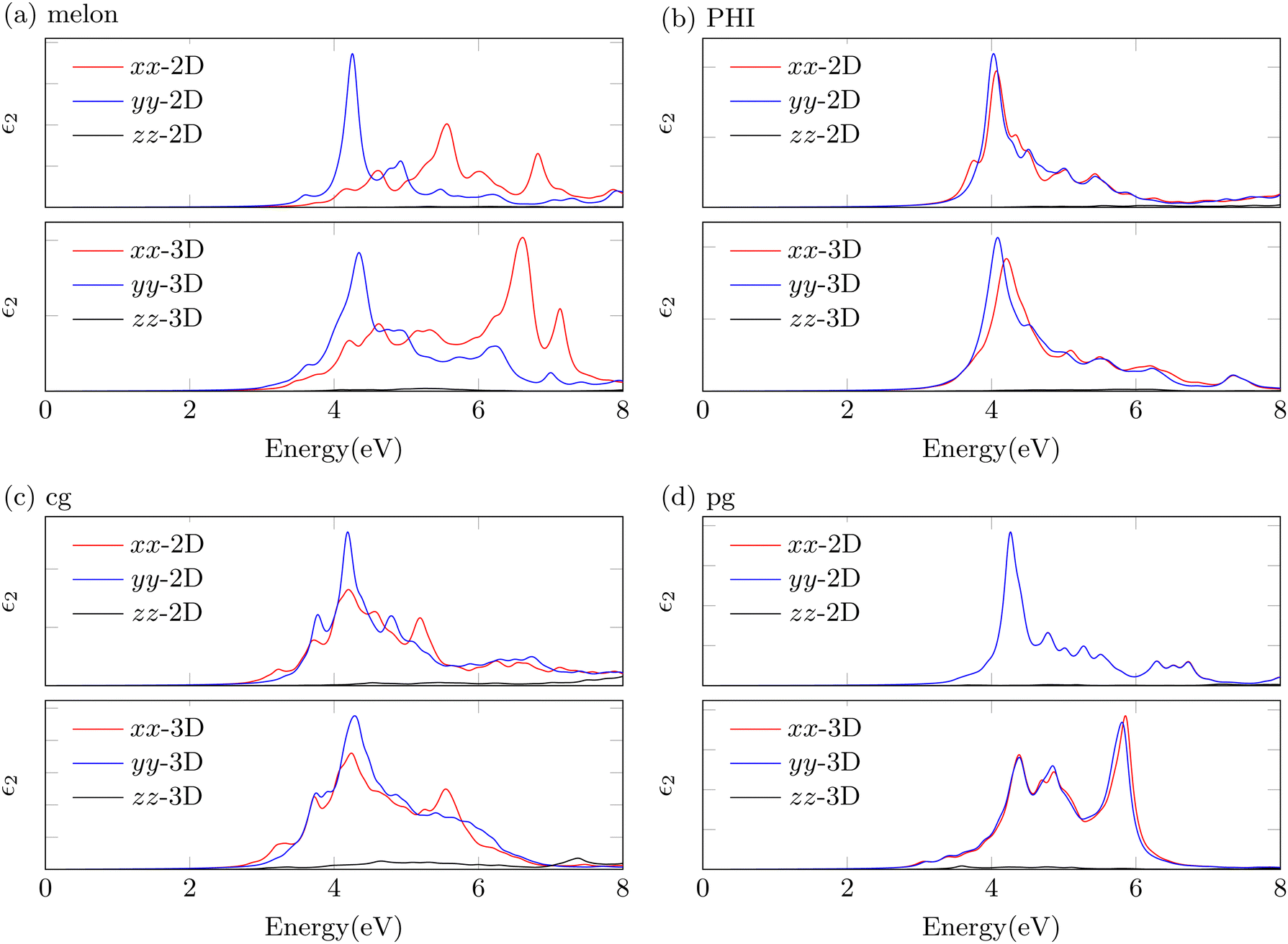 | ||
| Fig. 4 The imaginary part of the macroscopic dielectric functions of (a) melon, (b) PHI, (c) cg-CN, and (d) pg-CN structures on top of the TDHF@Casida method. Imaginary parts corresponding to the respective cartesian direction (xx, yy, zz), obtained by eqn (4) in the ESI,† are shown. | ||
The calculated imaginary parts reveal a prominent bright exciton consistently located near 310 nm (4.0 eV) in both 2D and 3D PCNs. For the wavelengths longer than 310 nm (<4.0 eV), multiple bright states are observed with relatively weak intensities, attributed to structural variations within the PCNs. Notably, as the transition occurs from 2D to 3D structures, the imaginary parts demonstrate an overall similarity, particularly near the band edges. Interestingly, when transitioning from 2D to 3D PCN structures, the imaginary parts demonstrate an overall similarity, particularly near the band edges. While interlayer interactions induce distinct changes in the band structure, the changes in optical properties remain minor due to their relatively weaker intensities compared to the absorption peaks near 4.0 eV. This observation illustrates that, despite the pronounced structural differences in PCN, the absorption behavior near the band edge yields only minor variations. Consequently, this explains the challenges of characterizing PCN microstructures from absorption spectra alone. Fig. 4 shows the imaginary part of dielectric functions for 2D and 3D melon structures, revealing distinct optical anisotropy.51,52 This distinctive feature reflects the linear structure characteristic of melon, raising considerations regarding its directional polarizability and potential limitations in optical efficiency.
Fig. 5 presents the average absorption spectra polarized in the respective spatial direction for 2D and 3D PCNs. We also provide the oscillator strength corresponding to the optical transition probability plotted against wavelength. Notably, a discrepancy between absorption spectra and oscillator strength indicates that calculated absorption encompasses transitions from different energy levels.53 This misalignment most likely contributes to the major disparity between the calculated absorption spectra of PCNs and experimental observations. In line with the imaginary part of the dielectric functions shown in Fig. 4, a strong oscillator strength is observed around 300 nm (approximately 4.1 eV) in both 2D and 3D structure models. This peak reflects the highest degenerate state of excited π electrons in C–N bonds within PCN structures (Fig. S2, ESI†). Additionally, the absorption peak and oscillator strength around 350 nm are linked to specific structural features. The intensity of this peak is pronounced in the buckled structures (PHI, cg) and shifts across structures, correlating with the degree of condensation within the PCN. Lastly, the absorption peak appearing around 400 nm (3.09 eV) is a consequence of interlayer interactions. This wavelength for the interlayer interactions is in good agreement with the literature observing the interplanar electron hopping in melon from transient absorption spectroscopy and transient photoluminescence using the pump wavelength of 388 nm.54 The peak intensity and patterns are also in agreement with the aforementioned PDOS results regarding the variation in interlayer interactions due to corrugations. Additionally, the absorption edge in each 2D structure undergoes a red shift in 3D structures. This red shift caused by interlayer overlap results in the formation of new peaks in melon (400 nm), cg-CN (400–450 nm), and pg-CN (450–500 nm), but it is not observed in the PHI structure.55 It is noteworthy that the subtle red shift observed in PHI can be attributed to the minimized interlayer interactions resulting from its structural flexibility. This structural adaptability allows the PHI structure to mitigate interactions, including interlayer interactions and the lone-pair repulsion of nitrogen atoms, by controlling interlayer spacing and local corrugation, respectively. Consequently, the PHI structure exhibits a remarkable independence between layers and heptazine units. The suggested independence between the different layers can be confirmed by the band structure in Fig. S1 (ESI†) and Fig. 3. When the PHI structure becomes 3D from 2D, the simple overlap of energy levels is exhibited near band edges. In contrast, the corrugated structure shows that one energy level moves upwards, while the others shift downward. It indicates that stronger interlayer interaction exists in the cg structure than in the case of the PHI structure. Additionally, the peaks ranging from 400–500 nm may provide the theoretical explanation that the forbidden transition, known as n–π transition, can be attributed to the graphitic regions. It is noted that these absorption peaks are specific to pure PCNs. This study does not consider interactions with other chemical species, such as radicals, charged, or heteroatom species, which might alter the behavior. The calculated absorption peaks for the PCN structural features are summarized in Table 1.
 | ||
| Fig. 5 The absorption spectra and oscillator strength were calculated for (a) melon, (b) PHI, (c) cg-CN, and (d) pg-CN in both 2D and 3D structures. The absorption spectra and oscillator strength of (e) mix1-3D and (f) mix2-3D, which depict the amorphous structure, are presented alongside the experimental values which is a dashed line. | ||
| Absorption feature | Attribution | |
|---|---|---|
| <300 nm | Degenerated π electrons | |
| Around 350 nm | Structural feature | Weak at melon and pg-CN, PHI (365 nm), cg-CN (375 nm) |
| Around 400 nm | Interlayer interaction | Melon (400 nm), cg-CN (400–450 nm), and pg-CN (450–500 nm) |
In our prior research, we introduced two microstructure patterns for PCNs, representing more amorphous configurations.33Fig. 5 illustrates the amorphous structures (inset) and their absorption spectra and oscillator strength. These two structures are virtual models that partially incorporate microstructures from melon (at the edge boundary), PHI, and graphitic structures. The mix1-3D structure contains minimal graphitic structures, positioned on both sides, while the mix2-3D structure features a larger graphitic region. Although neither structure fully replicates the experimental absorption spectra, our analysis suggests that the characteristic dimension of graphitic domains in the real-life PCN samples might be larger than in our mixed model structures. However, the agreement between our calculated results and the experimental data is still remarkably good. These results are also fully in line with experimental data from the literature that typically feature the fundamental absorption edge of ca. 2.7–2.9 eV.6,26,49 In this context, it should be noted that some experimentally observed PCN modifications with significantly shifted optical absorption (down to 600–700 nm) are typically the result of the presence of structural defects that can be produced during the synthesis, for example, by fragmentation of heptazine moieties.23 Interestingly, the most prominent bright excitons of the mix2-3D model, found around 375 nm, show remarkable agreement with the experimentally measured absorption spectra, particularly near the absorption edge. This suggests that the interlayer interactions present in the mix2-3D model might accidentally capture the characteristics of real-life PCN structures. This observation suggests that the absorption properties of actual PCNs are more related to the interlayer interactions between the graphitic regions and PHI-like or less condensed motifs (mix2-3D), rather than the interlayer interactions between the graphitic regions (mix1-3D). It may explain why stacking patterns of single-phase PCN structures have been unsuccessful in reproducing the experimentally observed absorption spectra. The findings can highlight the importance of considering the stacking patterns of diverse PCN microstructures to account for the interlayer electronic interactions in real-life PCN samples.
Interlayer interactions: influence on electronic and optical properties
Our results have consistently revealed the significant impact of interlayer interactions within PCN structures on their electronic structure and optical behavior near the band edge. Additionally, we have established that fundamental features, common to both 2D and 3D PCN structures, including the degenerate π–π* transition peak associated with C–N bonds, the structural characteristic peaks dependent on the degree of condensation, and interlayer overlap peaks, are consistently present in typical PCN materials. Based on these observations, potential photophysical processes occurring in both 2D and 3D PCNs are illustrated in Fig. 6a and b, respectively. In 2D PCNs, the electronic structure of a monolayer near the band edges can be categorized into two π states: π1 (localized π electron) and π2 (delocalized π electron), with a non-bonding (lone-pair) state positioned between them. The bright excitation near 300 nm can be explained by π–π* transitions governed by the Franck–Condon principle for vertical transitions. Corresponding energy transitions can exist in two forms, case 1 and case 3 in Fig. 6, encompassing a wider energy range than the bandgap. We claim that the excitons formed in this range represent hot carriers, supported by the fact that PCN absorption prominently occurs around 300 nm and 400 nm, while the primary emission converges at 450 nm. However, generic 2D PCN structures have limitations in explaining the discrepancy between the absorption and emission profiles of PCNs. This limitation occurs due to the absence of factors facilitating the relaxation of hot carriers. Instead, this energy range actually corresponds to bound exciton states, which enhance hot emission. This indicates that the 2D PCN structure can show not only the direct hot emissions (case 1 and case 3) but also the emission after the cooling of hot excitons (case 2 and case 4) simultaneously.47,56 This discrepancy implies that a single layer of PCN can exhibit substantially different exciton behavior when compared to multilayered PCNs.57 | ||
| Fig. 6 The proposed photophysical process of the general PCN materials in (a) 2D monolayer and (b) 3D stacked structures. The electron density at the respective energy level is illustrated below. The red corresponds to the absorption process, the blue is the photoluminescence process, the black is the non-radiative internal conversion, and the magenta is the interlayer energy/electron transfer, respectively. | ||
Consequently, the reported absorption patterns of PCNs so far suggest the presence of PCNs in a multilayered form. This is consistent with our previous study, which suggested that the stacking processes are thermodynamically favored over graphitic processes during the condensation reaction of PCN precursors.33 In the stacked 3D PCN structure, a more discrete energy structure can emerge, owing to the interplay between the 2D layers and the alignment of energy levels (Fig. 6). This characteristic indicates that the interlayer interactions within 3D structures can give rise to more complex excitonic processes. The proposed absorption profile exhibits a similar pattern to the 2D materials, with minor energy shifts, attributed to the independence of each layer. Remarkably, in 3D PCN structures, the cooling processes of hot carriers can gain prominence, derived by the overlaid π orbitals from the stacking. The orbital shapes corresponding to the respective energy levels are represented in Fig. 6. In the absorption spectra, the electrons and holes generated around 300 nm can undergo internal conversion more readily in the stacked 3D structure compared to the 2D structure. This phenomenon is attributed to the stabilization of the generated holes through the Coulombic interactions with electron orbitals in other layers. Consequently, Auger relaxation (case 6) and the relaxation of excited electrons due to screened holes (case 9) can be boosted in 3D structures.47 These factors offer fundamental insights into why PCNs exhibit multiple absorption peaks while displaying a prominent emission peak.
Based on the results so far, we assert that interlayer interactions play a pivotal role in the band edge properties of real PCN materials. Our calculations, in particular, highlight that the stacking indeed enables excited electrons, holes, and energy transport perpendicular to the layers. Thus, it is anticipated that tuning the interlayer interactions, such as modifying interlayer distances by introducing alkali ions, could indeed influence the exciton dynamics and also the related photocatalytic activity. This is supported by the fact that the generated electron/hole has sufficient orbital overlap with adjacent layers, and the interlayer spacing for electron transfer falls within the range of 3.2–3.4 Å, suggesting the potential for Förster or Dexter-type energy transfer, in accordance with Fermi's golden rule, as well as electron transfer.47 Furthermore, the 3D band structure in Fig. 3 reveals that the energy at Γ–Z or Γ–A directions (both are perpendicular to the plane) requires only 0.1–0.2 eV higher energy than the direct bandgap. These small energy barriers can be less meaningful if the cooling process of hot excitons is actually more pronounced in 3D structures. Significantly, this overlap of vertical orbitals selectively occurs at lone-pair N atoms in PCNs, implying that interlayer transitions can occur more effectively in the structures showing highly ordered crystallinity, rather than in amorphous PCNs. This could result in a slight blue shift in absorption/emission peaks. Additionally, the possibility of such interlayer interactions provides a basis for explaining cascade phenomena, electronic or ionic conductivity, recombination, and charge accumulation (particularly in the presence of cations) in PCNs or ionic PHI.58,59 For a more meticulous understanding of the electronic structure and corresponding optical properties in 3D structures, further theoretical studies are needed, encompassing electron–hole interactions. However, our present studies already underline the importance of interlayer interactions in PCNs and opens up avenues for future investigations for this intriguing class of materials.
Conclusion
In our study, we conducted the first-principles calculations to unravel the complex relationship between the microstructural attributes of PCN materials and their optical and electronic properties. This methodological approach allowed us to uncover distinctive electronic properties, underscoring the influence of condensation and corrugation degrees within PCN microstructures on their electronic and optical characteristics. The analysis distinctly highlights the correlation between absorption spectrum peaks and microstructural nuances, alongside the critical role of interlayer interactions in shaping these properties. Notably, our findings illuminate the stark differences in optical behavior between 2D and 3D PCN structures, pointing to the pivotal role of interlayer interactions in modulating properties near the band edges. This research underlines the presence of strongly localized electrons and the predominance of π electrons, associated with carbon–nitrogen bonds, as fundamental determinants of optical properties near the band edge in both 2D and 3D PCNs. Overall, this study highlights the significant influence of interlayer interactions on the near band edge properties of generic PCNs, which paves the way for manipulating the electronic and/or optical properties as well as charge dynamics in PCNs through rational microstructural engineering.Data availability
The data that support the findings of this study are available in the ESI† and all data used in this study is available via Zenodo.12 (DOI: https://doi.org/10.5281/zenodo.10844460).Conflicts of interest
There are no conflicts to declare.Acknowledgements
This work was funded by the Deutsche Forschungsgemeinschaft (DFG—German Research Foundation) through TRR 234 CataLight (project no. 364549901) as well as JA 1072/27-1 and BE 5102/5-1 (project no. 428764269). R. B. acknowledges funding from the European Union's Horizon Europe programme for research and innovation under grant agreement no. 101122061 (SUNGATE). The authors acknowledge support by the state of Baden-Württemberg through bwHPC and the German Research Foundation (DFG) through grant no INST 40/575-1 FUGG (JUSTUS 2 cluster). C. I. acknowledges the German Academic Exchange Service (DAAD, Ref. No. 91676720).References
- K. S. Novoselov, A. K. Geim, S. V. Morozov, D.-E. Jiang, Y. Zhang, S. V. Dubonos, I. V. Grigorieva and A. A. Firsov, Electric field effect in atomically thin carbon films, Science, 2004, 306, 666–669 CrossRef CAS PubMed.
- X. Wang, K. Maeda, X. Chen, K. Takanabe, K. Domen, Y. Hou, X. Fu and M. Antonietti, Polymer semiconductors for artificial photosynthesis: Hydrogen evolution by mesoporous graphitic carbon nitride with visible light, J. Am. Chem. Soc., 2009, 131, 1680–1681 CrossRef CAS PubMed.
- N. Mendelson, et al., Identifying carbon as the source of visible single-photon emission from hexagonal boron nitride, Nat. Mater., 2021, 20, 321–328 CrossRef CAS PubMed.
- H. Wang, Z. Du, Z. Cheng, Z. Cao, Y. Ye, Z. Wang, J. Wei, S. Wei, X. Meng, L. Song, Y. Gong, S. Yang and L. Guo, Ultralow-dielectric-constant Atomic Layers of Amorphous Carbon Nitride Topologically Derived from MXene, Adv. Mater., 2023, 35, 2301399 CrossRef CAS PubMed.
- X. Duan, C. Wang, A. Pan, R. Yu and X. Duan, Two-dimensional transition metal dichalcogenides as atomically thin semiconductors: opportunities and challenges, Chem. Soc. Rev., 2015, 44, 8859–8876 RSC.
- J. An, X. Zhao, Y. Zhang, M. Liu, J. Yuan, X. Sun, Z. Zhang, B. Wang, S. Li and D. Li, Perspectives of 2D materials for optoelectronic integration, Adv. Funct. Mater., 2022, 32, 2110119 CrossRef CAS.
- S. Zhang, Z. Xia, J. Meng, Y. Cheng, J. Jiang, Z. Yin and X. Zhang, Electronic and Transport Properties of InSe/PtTe2 van der Waals Heterostructure, Nano Lett., 2024, 24, 8402–8409 CrossRef CAS PubMed.
- H. Seksaria, A. Kishore and A. De Sarkar, Probing 2D Exciton Dynamics of Non-Hydrogenic Anisotropic Rydberg Spectra in Anomalous Screening Regime, J. Phys. Chem. C, 2024, 128, 6487–6495 CAS.
- B. Ma, G. Chen, C. Fave, L. Chen, R. Kuriki, K. Maeda, O. Ishitani, T. C. Lau, J. Bonin and M. Robert, Efficient Visible-Light-Driven CO2 Reduction by a Cobalt Molecular Catalyst Covalently Linked to Mesoporous Carbon Nitride, J. Am. Chem. Soc., 2020, 142, 6188–6195 CAS.
- S. N. Talapaneni, G. Singh, I. Y. Kim, K. AlBahily, A. H. Al-Muhtaseb, A. S. Karakoti, E. Tavakkoli and A. Vinu, Nanostructured Carbon Nitrides for CO2 Capture and Conversion, Adv. Mater., 2020, 32, 1–21 Search PubMed.
- I. Krivtsov, et al., Water-Soluble Polymeric Carbon Nitride Colloidal Nanoparticles for Highly Selective Quasi-Homogeneous Photocatalysis, Angew. Chem., Int. Ed., 2020, 59, 487–495 CAS.
- L. Lin, Z. Lin, J. Zhang, X. Cai, W. Lin, Z. Yu and X. Wang, Molecular-level insights on the reactive facet of carbon nitride single crystals photocatalysing overall water splitting, Nat. Catal., 2020, 3, 649–655 CAS.
- Z. Teng, Q. Zhang, H. Yang, K. Kato, W. Yang, Y. R. Lu, S. Liu, C. Wang, A. Yamakata, C. Su, B. Liu and T. Ohno, Atomically dispersed antimony on carbon nitride for the artificial photosynthesis of hydrogen peroxide, Nat. Catal., 2021, 4, 374–384 CAS.
- Y. Zhao, P. Zhang, Z. Yang, L. Li, J. Gao, S. Chen, T. Xie, C. Diao, S. Xi, B. Xiao, C. Hu and W. Choi, Mechanistic analysis of multiple processes controlling solardriven H2O2 synthesis using engineered polymeric carbon nitride, Nat. Commun., 2021, 12, 3701 CAS.
- Y. Xu, M. Fan, W. Yang, Y. Xiao, L. Zeng, X. Wu, Q. Xu, C. Su and Q. He, Homogeneous Carbon/Potassium-Incorporation Strategy for Synthesizing Red Polymeric Carbon Nitride Capable of Near-Infrared Photocatalytic H2 Production, Adv. Mater., 2021, 33, 2101455 CAS.
- H. Ou, S. Ning, P. Zhu, S. Chen, A. Han, Q. Kang, Z. Hu, J. Ye, D. Wang and Y. Li, Carbon Nitride Photocatalysts with Integrated Oxidation and Reduction Atomic Active Centers for Improved CO2 Conversion, Angew. Chem., Int. Ed., 2022, 61, e202206579 CrossRef CAS PubMed.
- Z. Wang, E. Almatrafi, H. Wang, H. Qin, W. Wang, L. Du, S. Chen, G. Zeng and P. Xu, Cobalt Single Atoms Anchored on Oxygen-Doped Tubular Carbon Nitride for Efficient Peroxymonosulfate Activation: Simultaneous Coordination Structure and Morphology Modulation, Angew. Chem., Int. Ed., 2022, 61, e202202338 CrossRef CAS PubMed.
- D. Zhang, et al., Photocatalytic Abstraction of Hydrogen Atoms from Water Using Hydroxylated Graphitic Carbon Nitride for Hydrogenative Coupling Reactions, Angew. Chem., Int. Ed., 2022, 61, e202204256 CrossRef CAS PubMed.
- J. Wu, Z. Liu, X. Lin, E. Jiang, S. Zhang, P. Huo, Y. Yan, P. Zhou and Y. Yan, Breaking through water-splitting bottlenecks over carbon nitride with fluorination, Nat. Commun., 2022, 13, 6999 CrossRef CAS PubMed.
- W. Xie, K. Li, X. H. Liu, X. Zhang and H. Huang, P-Mediated Cu–N4 Sites in Carbon Nitride Realizing CO2 Photoreduction to C2H4 with Selectivity Modulation, Adv. Mater., 2023, 35, 2208132 CrossRef CAS PubMed.
- T. Jia, D. Meng, R. Duan, H. Ji, H. Sheng, C. Chen, J. Li, W. Song and J. Zhao, Single-Atom Nickel on Carbon Nitride Photocatalyst Achieves Semihydrogenation of Alkynes with Water Protons via Monovalent Nickel, Angew. Chem., Int. Ed., 2023, 62, e202216511 CrossRef CAS PubMed.
- H. Inoki, G. Seo and K. Kanai, Synthesis of graphitic carbon nitride under low ammonia partial pressure, Appl. Surf. Sci., 2020, 534, 147569 CrossRef CAS.
- D. Mitoraj, I. Krivtsov, C. Li, A. Rajagopal, C. Im, C. Adler, K. Köble, O. Khainakova, J. Hniopek and C. Neumann, et al., A Study in Red: The Overlooked Role of Azo-Moieties in Polymeric Carbon Nitride Photocatalysts with Strongly Extended Optical Absorption, Chem. – Eur. J., 2021, 27, 17188–17202 CrossRef CAS PubMed.
- C. Adler, S. Selim, I. Krivtsov, C. Li, D. Mitoraj, B. Dietzek, J. R. Durrant and R. Beranek, Photodoping and Fast Charge Extraction in Ionic Carbon Nitride Photoanodes, Adv. Funct. Mater., 2021, 31, 2105369 CrossRef CAS.
- C. Adler, I. Krivtsov, D. Mitoraj, L. dos Santos-Gómez, S. García-Granda, C. Neumann, J. Kund, C. Kranz, B. Mizaikoff and A. Turchanin, et al., Sol-gel processing of water-soluble carbon nitride enables high-performance photoanodes, ChemSusChem, 2021, 14, 2170–2179 CAS.
- C. Pulignani, C. A. Mesa, S. A. Hillman, T. Uekert, S. Giménez, J. R. Durrant and E. Reisner, Rational design of carbon nitride photoelectrodes with high activity toward organic oxidations, Angew. Chem., Int. Ed., 2022, 134, e202211587 Search PubMed.
- M. Z. Rahman, P. C. Tapping, T. W. Kee, R. Smernik, N. Spooner, J. Moffatt, Y. Tang, K. Davey and S.-Z. Qiao, A benchmark quantum yield for water photoreduction on amorphous carbon nitride, Adv. Funct. Mater., 2017, 27, 1702384 Search PubMed.
- M. Z. Rahman and C. B. Mullins, Understanding charge transport in carbon nitride for enhanced photocatalytic solar fuel production, Acc. Chem. Res., 2018, 52, 248–257 CrossRef PubMed.
- R. Godin, Y. Wang, M. A. Zwijnenburg, J. Tang and J. R. Durrant, Time-Resolved Spectroscopic Investigation of Charge Trapping in Carbon Nitrides Photocatalysts for Hydrogen Generation, J. Am. Chem. Soc., 2017, 139, 5216–5224 CAS.
- W. Wei and T. Jacob, Strong excitonic effects in the optical properties of graphitic carbon nitride g-C3N4 from first principles, Phys. Rev. B:Condens. Matter Mater. Phys., 2013, 87, 085202 Search PubMed.
- S. Melissen, T. Le Bahers, S. N. Steinmann and P. Sautet, Relationship between Carbon Nitride Structure and Exciton Binding Energies: A DFT Perspective, J. Phys. Chem. C, 2015, 119, 25188–25196 CAS.
- G. Zhang, G. Li, Z.-A. Lan, L. Lin, A. Savateev, T. Heil, S. Zafeiratos, X. Wang and M. Antonietti, Optimizing optical absorption, exciton dissociation, and charge transfer of a polymeric carbon nitride with ultrahigh solar hydrogen production activity, Angew. Chem., Int. Ed., 2017, 129, 13630–13634 Search PubMed.
- C. Im, B. Kirchhoff, I. Krivtsov, D. Mitoraj, R. Beranek and T. Jacob, Structure and optical properties of polymeric carbon nitrides from atomistic simulations, Chem. Mater., 2023, 35, 1547–1559 CAS.
- F. K. Kessler, Y. Zheng, D. Schwarz, C. Merschjann, W. Schnick, X. Wang and M. J. Bojdys, Functional carbon nitride materials—design strategies for electrochemical devices, Nat. Rev. Mater., 2017, 2, 17030 CAS.
- B. Schulze Lammers, N. López-Salas, J. Stein Siena, H. Mirhosseini, D. Yesilpinar, J. Heske, T. D. Kühne, H. Fuchs, M. Antonietti and H. Mönig, Real-Space Identification of Non-Noble Single Atomic Catalytic Sites within Metal-Coordinated Supramolecular Networks, ACS Nano, 2022, 16, 14284–14296 CAS.
- Q. Xie, C. Wang, W. Shen, Y. Fu and Y. Si, Regulating Intermediate Concentration to Synthesize Highly Crystalline g-C3N4 under Spontaneous Ultrahigh Pressure, ChemNanoMat, 2023, 9, e202300102 CAS.
- M. Feierabend, S. Brem and E. Malic, Optical fingerprint of bright and dark localized excitonic states in atomically thin 2D materials, Phys. Chem. Chem. Phys., 2019, 21, 26077–26083 CAS.
- S. An, G. Zhang, K. Li, Z. Huang, X. Wang, Y. Guo, J. Hou, C. Song and X. Guo, Self-Supporting 3D Carbon Nitride with Tunable n → π* Electronic Transition for Enhanced Solar Hydrogen Production, Adv. Mater., 2021, 33, 2104361 CAS.
- Q. Gao, X. Zhuang, S. Hu and Z. Hu, Corrugation Matters: Structure Models of Single Layer Heptazine-Based Graphitic Carbon Nitride from First-Principles Studies, J. Phys. Chem. C, 2020, 124, 4644–4651 CAS.
- Q. Xu, Z. Xia, J. Zhang, Z. Wei, Q. Guo, H. Jin, H. Tang, S. Li, X. Pan and Z. Su, et al., Recent advances in solar-driven CO2 reduction over g-C3N4-based photocatalysts, Carbon Energy, 2023, 5, e205 CAS.
- M. Re Fiorentin, F. Risplendi, M. Palummo and G. Cicero, First-Principles Calculations of Exciton Radiative Lifetimes in Monolayer Graphitic Carbon Nitride Nanosheets: Implications for Photocatalysis, ACS Appl. Nano Mater., 2021, 4, 1985–1993 CAS.
- Z. Wei, M. Liu, Z. Zhang, W. Yao, H. Tan and Y. Zhu, Efficient visible-light-driven selective oxygen reduction to hydrogen peroxide by oxygen-enriched graphitic carbon nitride polymers, Energy Environ. Sci., 2018, 11, 2581–2589 CAS.
- L. Jing, R. Zhu, D. L. Phillips and J. C. Yu, Effective Prevention of Charge Trapping in Graphitic Carbon Nitride with Nanosized Red Phosphorus Modification for Superior Photo(electro)catalysis, Adv. Funct. Mater., 2017, 27, 1703484 Search PubMed.
- Q. Ruan, T. Miao, H. Wang and J. Tang, Insight on Shallow Trap States-Introduced Photocathodic Performance in n-Type Polymer Photocatalysts, J. Am. Chem. Soc., 2020, 142, 2795–2802 CrossRef CAS PubMed.
- A. J. Rieth, Y. Qin, B. C. Martindale and D. G. Nocera, Long-Lived Triplet Excited State in a Heterogeneous Modified Carbon Nitride Photocatalyst, J. Am. Chem. Soc., 2021, 143, 4646–4652 CAS.
- C. Pulignani, C. A. Mesa, S. A. Hillman, T. Uekert, S. Giménez, J. R. Durrant and E. Reisner, Rational Design of Carbon Nitride Photoelectrodes with High Activity Toward Organic Oxidations, Angew. Chem., Int. Ed., 2022, 61, e202211587 CrossRef CAS PubMed.
- V. Balzani; P. Ceroni and A. Juris, Photochemistry and photophysics: concepts, research, applications, John Wiley & Sons, 2014 Search PubMed.
- P. Kubelka and F. Munk, An article on optics of paint layers, Z. Tech. Phys., 1931, 12, 259–274 Search PubMed.
- C. Merschjann, T. Tyborski, S. Orthmann, F. Yang, K. Schwarzburg, M. Lublow, M.-C. Lux-Steiner and T. Schedel-Niedrig, Photophysics of polymeric carbon nitride: An optical quasimonomer, Phys. Rev. B:Condens. Matter Mater. Phys., 2013, 87, 205204 CrossRef.
- C. Im, R. Beranek and T. Jacob, Structural Influence on Exciton Formation and the Critical Role of Dark Excitons in Polymeric Carbon Nitrides, Adv. Energy Mater., 2025 DOI:10.1002/aenm.202405549.
- C. Li, C. Adler, I. Krivtsov, D. Mitoraj, R. Leiter, U. Kaiser, R. Beranek and B. Dietzek, Ultrafast anisotropic exciton dynamics in a water-soluble ionic carbon nitride photocatalyst, Chem. Commun., 2021, 57, 10739–10742 RSC.
- P. Giusto, B. Kumru, D. Cruz and M. Antonietti, Optical anisotropy of carbon nitride thin films and photografted polystyrene brushes, Adv. Opt. Mater., 2022, 10, 2101965 CrossRef CAS.
- R. Ruger, E. Van Lenthe, Y. Lu, J. Frenzel, T. Heine and L. Visscher, Efficient calculation of electronic absorption spectra by means of intensity-selected time-dependent density functional tight binding, J. Chem. Theory Comput., 2015, 11, 157–167 CrossRef PubMed.
- C. Merschjann, S. Tschierlei, T. Tyborski, K. Kailasam, S. Orthmann, D. Hollmann, T. Schedel-Niedrig, A. Thomas and S. Lochbrunner, Complementing Graphenes: 1D Interplanar Charge Transport in Polymeric Graphitic Carbon Nitrides, Adv. Mater., 2015, 27, 7993–7999 CAS.
- G. Chen, Z. D. Zhang, Y. X. Liao, Z. Zhang and Y. Z. You, Modulating Local Charge Distribution of Carbon Nitride for Promoting Exciton Dissociation and Charge-Induced Reactions, Small, 2021, 17, 2100698 CAS.
- H. Wang, X. Sun, D. Li, X. Zhang, S. Chen, W. Shao, Y. Tian and Y. Xie, Boosting Hot-Electron Generation: Exciton Dissociation at the Order-Disorder Interfaces in Polymeric Photocatalysts, J. Am. Chem. Soc., 2017, 139, 2468–2473 CAS.
- D. Y. Qiu, G. Cohen, D. Novichkova and S. Refaely-Abramson, Signatures of dimensionality and symmetry in exciton band structure: Consequences for exciton dynamics and transport, Nano Lett., 2021, 21, 7644–7650 CAS.
- K. L. Corp and C. W. Schlenker, Ultrafast Spectroscopy Reveals Electron-Transfer Cascade That Improves Hydrogen Evolution with Carbon Nitride Photocatalysts, J. Am. Chem. Soc., 2017, 139, 7904–7912 CAS.
- J. Kröger, F. Podjaski, G. Savasci, I. Moudrakovski, A. Jiménez-Solano, M. W. Terban, S. Bette, V. Duppel, M. Joos, A. Senocrate, R. Dinnebier, C. Ochsenfeld and B. V. Lotsch, Conductivity Mechanism in Ionic 2D Carbon Nitrides: From Hydrated Ion Motion to Enhanced Photocatalysis, Adv. Mater., 2022, 34, 2107061 Search PubMed.
Footnote |
| † Electronic supplementary information (ESI) available. See DOI: https://doi.org/10.1039/d5tc01121c |
| This journal is © The Royal Society of Chemistry 2025 |