
Passivation of defects by tetrafluoroterephthalonitrile introduced into MAPbI3 for high-performance perovskite photodetectors†
Yuanhao
Li
a,
Yukun
Wang
 *a,
Zuhuan
Lu
a,
Zongming
Yu
a,
Tianyi
Zhang
a and
Wenhong
Sun
*abcd
*a,
Zuhuan
Lu
a,
Zongming
Yu
a,
Tianyi
Zhang
a and
Wenhong
Sun
*abcd
aResearch Center for Optoelectronic Materials and Devices, Guangxi Key Laboratory for the Relativistic Astrophysics, School of Physical Science and Technology, Guangxi University, Nanning 530004, China. E-mail: ykwang0929@163.com
bState Key Laboratory of Featured Metal Materials and Life-cycle Safety for Composite Structures, Guangxi University, Nanning 530004, China
cMOE Key Laboratory of New Processing Technology for Nonferrous Metals and the Guangxi Key of Processing for Non-ferrous Metals and Featured Materials, Guangxi University, Nanning 530004, China
dThird Generation Semiconductor Industry Research Institute, Guangxi University, Nanning 530004, China
First published on 28th April 2025
Abstract
Methylammonium lead iodide is widely used in the preparation of photodetectors because of its excellent photovoltaic properties. However, because of the nature of the perovskite polycrystals, the low-temperature solution treatment approach of creating perovskite thin films causes flaws to arise in the material. Undercoordinated lead ions (Pb2+) have been shown to have comparatively low formation energies among all defect species and to be a major contributor to defect creation. Here, we use a straightforward but efficient additive engineering strategy to introduce tetrafluoroterephthalonitrile as an additive into the perovskite precursor solution to passivate perovskite defects and improve the quality of perovskite thin films for the production of high-efficiency perovskite photodetectors. We demonstrated that –CN (cyano) and polyfluorine atoms in the structure of TFTPN may passivate defects caused by lead ions and prevent the releasing of organic cations (MA+), improving the stability of the perovskite structure and the quality of perovskite films. Consequently, we designed perovskite photodetectors with TFTPN that demonstrated exceptional performance in terms of photoresponse, detection and other areas. These devices had a maximum peak external quantum efficiency (EQE) of 91.73%, a lower dark current density of 8.86 × 10⁻¹¹ A cm−2, a linear dynamic range (LDR) of 105.4 dB, and more. Furthermore, the perovskite photodetector's durability is enhanced by the addition of TFTPN, and after 20 days of storage in an air environment at 25 °C and 20–30% relative humidity, the device retains its original efficiency of 92.3%.
Introduction
In recent years, organic–inorganic metal halide perovskite materials have been widely and importantly developed for solar cells, light emitting diodes and photodetectors due to their excellent photovoltaic properties and easy processing advantages.1–3 Preparation of perovskite films by low-temperature solution treatment is the easiest way.4–6 However, this method is prone to the formation of a large number of ionic defects in the perovskite films.7–9 It has been shown that the defects mainly originate from under-coordinated lead ions (Pb2+) and free organic cations.10–12 In order to effectively passivate the defects, the researchers introduced a variety of small-molecule additives containing functional groups with significant electronegativity, such as nitrogen (N), oxygen (O), and sulfur (S), into the perovskite solution. These additives can effectively coordinate with the Pb2+ sites in the perovskite, thereby enhancing the overall quality and photovoltaic performance of the film.13–15 These molecules may interact with Pb ions. Li et al. demonstrated that the presence of the –COOH (carboxylic acid) moiety enabled the organic dye molecule, AQ310, to attach to the under-coordinated Pb2+ on the perovskite surface, interacting and successfully passivating the defects.16 Zheng's group added a substance called 3-(decyldimethylammonio)-propane-sulfonate inner salt to the perovskite precursor's solution. This molecule has a strong coordination connection with Pb2+, and this contact effectively prevents defects from forming during perovskite processing. Furthermore, the compound's positively and negatively charged characteristics enable it to neutralize the perovskite's charged flaws, improving the material's qualities even more. Interestingly, it demonstrated outstanding photostability.17 Wang's team creatively mixed the ionic liquid BMIMSCN with the perovskite precursor solution. As a result of this effort, the ionic solution and Pb2+ formed a new Pb–N bond. The crystalline quality of the perovskite films was improved by the creation of this chemical link, which also greatly decreased the amount of defects in the films. This enhancement not only prolongs the carrier lifespan but also improves the devices' overall performance.18According to our findings, the TFTPN structure's –CN (cyano) and multi-fluorine atoms may passivate lead ion-induced defects and stop organic cations from escaping, boosting the perovskite structure's stability and the perovskite film's quality. In all, we designed a photodetector with a linear dynamic range (LDR) of up to 105.4 dB, a lower dark current density of 8.86 × 10⁻¹¹ A cm−2, and a maximum peak external quantum efficiency (EQE) of 91.73%. The stability was enhanced, and the device retained 92.3% of its original efficiency after 20 days of storage in an air surrounding with a temperature of 25 °C and a relative humidity of 20–30%.
Results and discussion
Here, we introduce tetrafluoroterephthalonitrile (TFTPN) in the perovskite film. The preparation process is shown in Fig. 1a. Tetrafluoroterephthalonitrile, was an original addition to the perovskite precursor solution that we utilized to improve the quality of the perovskite films and passivate their flaws. TFTPN's molecular structure, which includes many F atoms and cyano (–CN), is displayed in Fig. 1c. To investigate the activity impacts of the –CN and F functional groups in the TFTPN molecule, we analyzed its electronegativity using an electrostatic surface potential (ESP) diagram, as shown in Fig. 1d. These functional groups form different charged environments around the molecule due to their different chemical properties, generating electron-rich and electron-deficient regions, which are favorable for passivation defects.19 The dark brown region in the image highlights the two –CN groups' strong electronegativity in the TFTPN molecule, demonstrating the extremely effective passivation of the electron-rich –CN groups for Pb2+ defects.20 Furthermore, the additive molecule's F atoms all contain concentrations of negative charge, indicating that they all help form hydrogen–fluorine interactions with organic cations.21,22 Consequently, the passivation mechanism is depicted in Fig. 1b upon the introduction of TFTPN additive molecules into the perovskite system. | ||
| Fig. 1 (a) Schematic illustration of TFTPN templated perovskite fabrication process. (b) Schematic diagram of the interaction between TFTPN and perovskite. (c) Structural formula of TFTPN. (d) ESP distribution maps of TFTPN. | ||
To verify the above results in more depth, we performed X-ray photoelectron spectroscopy (XPS) analysis of the perovskite films with or without TFTPN molecules based on the structure as ITO/NiOX/MAPbI3. Here, for ease of presentation, we define the ideal doping concentration as 2 mg mL−1, due to the fact that a large number of studies have shown that a doping concentration of 2.0 mg mL−1 gives the highest efficiency of a perovskite photodetector; the ideal concentration is used for the characterization, unless otherwise stated. Analyzing the with TFTPN encapsulated thin films using XPS, the C 1s-core spectra revealed distinct –CN (285.93 eV) and C–F (289.03 eV) bonding signals (Fig. 2a), demonstrating that TFTPN molecules were successfully incorporated into the ref. 23–25. Meanwhile, the results of energy dispersive X-ray spectroscopy (EDS) showed the N and F elements, which confirmed the above results (Fig. 2b, c and Fig. S1a–c, ESI†). These results provide strong support for subsequent performance tests and mechanistic studies. The addition of –CN groups probably increased the electron cloud density of Pb2+, which is why the peaks of Pb2+ were moved toward lower binding energies after the additive was added.20 The primary peaks that were initially situated at 143.16 eV (Pb 4f5/2) and 138.29 eV (Pb 4f7/2) were both moved toward the low binding energy region (i.e., 142.75 eV corresponds to Pb 4f5/2, and 137.89 eV corresponds to Pb 4f7/2) following TFTPN modification, as can be seen in the XPS spectral curves displayed in Fig. 2d. This result suggests that the strong interaction exists between the –CN group in TFTPN and the undercoordinated Pb2+ ions in the perovskite membrane. Both the I 3d and N 1s spectra revealed a notable shift toward lower binding energies in the membranes changed by TFTPN, as illustrated in Fig. 2e and f. By forming coordination links between TFTPN and I− and MA+ sites, this shift event efficiently lowers the number of defects on the perovskite surface.26 This outcome further demonstrates TFTPN's exceptional capacity to prevent the formation of defects and restore the surface structure of perovskite thin films.27
 | ||
| Fig. 2 (a) XPS spectra of C 1s of MAPbI3 with TFTPN. (b) EDS image of F. (c) EDS image of N. (d) Pb 4f orbital XPS spectra. (e) I 3d orbital XPS spectra. (f) N 1s orbital XPS spectra. | ||
In addition, we hypothesized that F− in TFTPN could form a hydrogen bond with the charged MA+, and the above N 1s peak was shifted to the direction of low binding energy, which indicated a charge transfer on the N–H unit of the MA+, and since F− has a strong electronegativity, such a shift may imply the formation of a hydrogen bond between F− and MA+.11,28 This was verified in our 1H NMR characterization, as shown in Fig. S3 and S4 (ESI†). In pure deuterated DMSO solution, the resonance signal of protonated ammonium in MAI can be observed to be located at 7.49 ppm.29 However, after TFTPN modification, the resonance signal of ammonium splits at both 7.49 ppm and 7.56 ppm, forming two distinct peaks. This occurrence implies that the chemical environment of ammonium in MA+ is changed by the interaction between the addition of TFTPN and MA+, leading to two distinct states.30 The creation of hydrogen bonds between F− and MA+ efficiently prevents the movement of MA+.31–34
Subsequently, we verified the chemical interaction between TFTPN and lead iodide by Fourier transform infrared spectroscopy (FTIR) analysis. In the FTIR spectrum of TFTPN (Fig. S5, ESI†), peaks located at 2252 cm−1 and 1260 cm−1 were observed, which corresponded to the stretching vibrations of the C–N and C–F bonds, respectively, and the peak at 1500 cm−1 was attributed to the stretching vibration of the C–C aromatic bond.35–37 Notably, these distinctive peaks can also be found in the TFTPN–PbI2 spectrum. The effective binding of TFTPN to PbI2 to create the TFTPN–PbI2 complex is strongly supported by this discovery.
The above findings reveal that additive TFTPN is capable of forming strong ligand and hydrogen bonds with the perovskite material, and we expect that these strong interactions will have a significant optimizing effect on the morphology of the modified perovskite films. To confirm this, we used scanning electron microscopy (SEM) and atomic force microscopy (AFM) on substrates with the structure of ITO/NiOX/MAPbI3 to thoroughly examine the surface morphology of the perovskite films with or without TFTPN. The cross-section of the ITO/NiOX/MAPbI3 structure with TFTPN (Fig. 3a). As shown in Fig. 3b–e, the surface morphology of the TFTPN additive-modified perovskite films is flatter and denser, with fewer pinholes and a significant increase in grain size. From Fig. 3f and g, we counted the grain size. The average grain size of perovskite films before modification was 205 nm, while the average grain size of the modified films increased to 247 nm. This indicates that the TFTPN additive significantly increased the average grain size of perovskite films. Additionally, as illustrated in Fig. 3h and i, the root-mean-square (RMS) of perovskite films surface roughness with TFTPN decreased to 13.5 nm, a 10.4 nm decrease from the unaltered control films' roughness of 23.9 nm. In summary, the introduction of the additive TFTPN not only improves the morphology of perovskite films but also provides an effective way to prepare high-quality perovskite films by increasing the grain size and reducing the surface roughness.
 | ||
| Fig. 3 (a) Cross-sectional SEM image of structure ITO/NiOX/MAPbI3 with TFTPN. (b)–(e) SEM images of perovskite. (f) and (g) Perovskite grain size statistics at 500 nm scale. (h) and (i) AFM images of perovskite. | ||
To obtain a better understanding of how additive introduction affects perovskite crystal formation, we used X-ray diffraction (XRD) to compare the growth of perovskite crystals with and without TFTPN. Fig. 4a shows the XRD patterns of perovskite films prepared in MAPbI3-based perovskite precursor solution with TFTPN additions of 0, 0.5, 1.0, 2.0, and 3.0 mg mL−1, respectively. No discernible peak displacement was seen, and all films had a dominating (110) peak at 14.6°, confirming that the perovskite lattice structure was not negatively impacted by the addition of TFTPN. Notably, the perovskite film exhibited the strongest diffraction intensity of the (110) peak when the TFTPN addition was 2 mg mL−1. The results showed that the (110) peak at 14.6° of the perovskite film with TFTPN was not only significantly enhanced in intensity, but also its full width at half peak (FWHM) was significantly narrower (Fig. 4b and c). This finding strongly suggests that the introduction of TFTPN effectively enhances the crystalline quality of the perovskite film.38 The findings of this XRD examination are in excellent agreement with our earlier findings from SEM, which both demonstrate that TFTPN positively promotes the development of perovskite. Based on previous studies, we postulated that the interaction of TFTPN with Pb2+ ions in perovskite precursor solution at the surface of the colloidal particles would be a significant factor influencing the formation of calixarene.39 We used dynamic light scattering (DLS) measurements to confirm this, and the outcomes are displayed in Fig. 4d. We observed a change in the colloidal particle radius distribution in perovskite precursor solution with TFTPN compared to the control sample. The radius of colloidal particles was Gaussian distributed, and the average size of colloidal particles with TFTPN was about 904 nm, while the average size of colloidal particles of control samples was about 1174 nm (Fig. 4e and f). This change may be attributed to the interaction of the TFTPN additive with the colloidal particles in the precursor solution. In particular, TFTPN might coordinate with Pb2+ ions as a ligand, changing the colloidal particles' surface characteristics. The bigger colloidal particles may be “trimmed” into smaller ones by this coordination, which could have an impact on the perovskites' growth process.40 The above DLS measurements further confirm that the introduction of TFTPN plays a key role in the growth and film formation of perovskites. Since the quality of perovskite film formation directly affects its light absorption efficiency, by optimizing the addition of TFTPN, we can expect to obtain higher-quality perovskite films, which will improve the performance of related optoelectronic devices.
 | ||
| Fig. 4 (a) XRD spectra of perovskite films doped with different concentrations of TFTPN. (b) and (c) The FWHM and peak intensity for (110) plane of perovskite. (d) Size distributions of complexes in complex precursor (with/without TFTPN) system detected by dynamic light scattering. (e) and (f) Size statistics of perovskite with and without TFTPN. (g) UV-vis absorption spectra of perovskite films doped with different concentrations of TFTPN. (h) Tauc curve of perovskite film with and without TFTPN. (i) Urbach energy. | ||
Thus, we employed ultraviolet-visible spectroscopy (UV-vis) to thoroughly examine the precise impact of TFTPN on the light absorption capabilities of perovskite films on devices with the ITO/NiOX/MAPbI3 structure (Fig. 4g). According to the conclusions, the TFTPN-modified perovskite films have noticeably higher light absorption in the 530–780 nm wavelength range. This is a clear sign that the growth quality of the perovskite crystals has been effectively improved. To more accurately assess the effect of TFTPN modification on the band gap (Eg) of perovskite thin films, we analyzed it by plotting Tauc plots (i.e., Ahν2versus hν) based on UV-vis spectroscopic data (Fig. 4h). Due to the analytical data, the TFTPN-modified perovskite film's band gap is approximately 1.589 eV, which is smaller than that of the control without surface treatment (1.597 eV). In addition, to further assess the quality of the perovskite films, we calculated the Urbach energy (EU) using the formula:41,42
ln![[thin space (1/6-em)]](https://www.rsc.org/images/entities/char_2009.gif) α = lnα0 + (hν/EU) α = lnα0 + (hν/EU) | (1) |
The improvement in the quality of perovskite films has a positive impact on the extraction and transport of photogenerated carriers. To this end, we performed steady-state (PL) and time-resolved photoluminescence (TRPL) spectroscopic tests for ITO/NiOX/(0, 0.5, 1.0, 2.0, and 3.0 mg mL−1 TFTPN: MAPbI3) structures to probe the carrier extraction properties of perovskite samples at the NiOX/MAPbI3 interface. In comparison to the unmodified MAPbI3 films, the TFTPN-modified films gradually decreased in PL intensity under 532 nm laser illumination, as seen in Fig. 5a. The perovskite film doped with 2 mg mL−1 TFTPN had the lowest PL intensity among all. The reduction in PL intensity suggests that holes are extracted more quickly at the NiOX/MAPbI3 interface, further demonstrating the better PL quenching efficiency and more efficient carrier transport capacity of TFTPN-modified treated perovskite films at the NiOX interface.44 Next, we observed the TRPL image, which was fitted by a double-exponential decay function:45
| y = A1e(−t/τ1) + A2e(−t/τ2) + y0 | (2) |
 | (3) |
 | ||
| Fig. 5 (a) Steady-state PL spectra of perovskite films doped with different concentrations of TFTPN. (b) Time-resolved PL decay plots of perovskite films doped with different concentrations of TFTPN. | ||
The TRPL data revealed that the device at the optimal concentration (39.40 ns) had the shortest decay lifetime when compared to the control device (119.83 ns), based on the specific data values displayed in Table 1. This finding implies that photoinduced carriers have the ability to migrate swiftly from the cluster to NiOX.46 This outcome is in line with previous PL test finding. The creation of stable and high-performing perovskite photodetectors is strongly supported by these observations, which collectively show the superior photovoltaic qualities and stability of premium perovskite films.
| Concentration (mg mL−1) | τ 1 (ns) | A 1 (%) | τ 2 (ns) | A 2 (%) | τ avg (ns) |
|---|---|---|---|---|---|
| 0 | 5.36 | 2.20 | 141.94 | 0.43 | 119.83 |
| 0.5 | 6.25 | 1.64 | 101.74 | 0.49 | 85.45 |
| 1.0 | 2.93 | 7.85 | 79.56 | 0.41 | 47.87 |
| 2.0 | 3.47 | 5.62 | 71.33 | 0.29 | 39.40 |
| 3.0 | 3.96 | 3.74 | 104.89 | 0.35 | 75.88 |
A schematic representation of the planar inverted perovskite photodetectors (PDs) with ITO/NiOX/MAPbI3 (with and without TFTPN)/C60/BCP/Cu structure is provided in Fig. 6a. This model was built to thoroughly examine the precise impact of TFTPN additions on the device performance. External quantum efficiency (EQE) is an important indicator of photoelectric conversion efficiency, which is expressed as the ratio of the number of electrons collected by the photodetector to the number of incident photons and can be expressed as:47
 | (4) |
 | ||
| Fig. 6 (a) Device structure diagram. (b) EQE response curves of PDS doped with or without TFTPN. (c) Statistical distribution of EQE for PDS doped with or without TFTPN. (d) Responsivity curves of PDS doped with or without TFTPN. (e) Detectivity curves of PDS doped with or without TFTPN. (f) LDR of PDS doped with or without TFTPN. (g) Dark current density curves of PDS doped with or without TFTPN. (h) SCLC plots of the hole-only device doped with or without TFTPN. (i) SCLC plots of the electron-only device doped with or without TFTPN. | ||
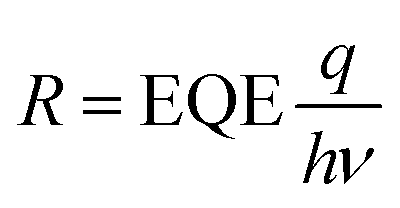
Here, we introduce the responsivity and specific detectivity parameters to further evaluate effective capture of light by photodetectors with or without TFTPN. The responsivity (R) reflects the efficiency of the PDs to respond to different intensities of incident light and can be expressed as:48
 | (5) |
Specific detectivity (D*) is a measure of the photodetector's ability to detect weak light signals. When the noise of the detector is mainly due to grain noise, D* can be expressed as:49
 | (6) |
Linear dynamic range (LDR) is a core performance metric of photodetectors, which reflects the wide interval over which the photodetector can accurately detect and quantify the intensity of the optical signal, defined as:50
 | (7) |
The excellent performance of the devices in terms of EQE, responsivity, and specific detectivity indicated that the incorporation of TFTPN effectively passivated the defects in the perovskite structure. To further investigate the effect of doping with TFTPN doped in the perovskite on the passivation of the defects in the perovskite photodetectors, the J–V characteristics of the photodetectors doped with and without TFTPN were measured in dark conditions. J–V characteristics of perovskite photodetectors (Fig. 6g), the dark current densities of photodetectors with TFTPN were all lower than those of photodetectors without TFTPN under 0 V bias (Table S2, ESI†), and PDs with TFTPN decreased from 5.24 × 10⁻⁹ A cm−2 to 8.86 × 10⁻¹¹ A cm−2 compared to PDs without TFTPN. The results show that the introduction of TFTPN can effectively promote the formation of high-quality perovskite films with low defect density.
To quantitatively evaluate the passivation effect of TFTPN on perovskite films, the defect density of TFTPN on perovskite films was calculated using the space charge limiting current (SCLC) method. A schematic of the hole-only device, which consists of these functional layers including ITO/NiOX/MAPbI3/Spiro-OMeOxide/MoO3/Cu, is illustrated in Fig. 6h. The defect density can be calculated by the following equation:20,51
 | (8) |
One of the main elements influencing the performance of photodetectors is the transit efficiency of photogenerated carriers. Accelerated transient photocurrent rise and fall periods typically indicate faster and more effective carrier transportation within the device. The photodetector's transient photocurrent was measured using both the photodetectors with or without TFTPN under 520 nm light irradiation. As shown in Fig. 7a and b, PDs outstanding and steady dynamic response is demonstrated by the photocurrent curves, which show no discernible attenuation of the photocurrent after multiple cycles of testing under continuous 1 KHz light irradiation. The rise time is the time required for the photocurrent to rise from 10% to 90% of the maximum value, while the fall time is the time required for the photocurrent to fall from 90% to 10% of the maximum value.52 The rise and fall times of the control device are 166 μs and 20 μs, respectively, while the rise and fall times of the wTFTPN device are 122 μs and 20 μs, respectively, and the response time of the optimal device becomes faster after the TFTPN modification treatment.
 | ||
| Fig. 7 (a) Transient photocurrents of PDs doped with or without TFTPN under multiple cycles at 1 kHz light. (b) Transient photocurrents of PDS doped with or without TFTPN under a single cycle at 1 kHz light. (c) Stability of PDs doped with or without TFTPN stored for 20 days at temperature ∼25 °C and relative humidity 20–30%. (d) Water contact angle of perovskite doped with or without TFTPN. | ||
For photodetectors, having excellent photoelectric performance is not enough to be called an excellent photodetector, and stability is another key aspect of photodetectors. Subsequently, the unencapsulated devices were subjected to a 20-day stability test in air (20–30% relative humidity, 25 °C), as shown in Fig. 7c. After 20 days, we found that the EQE values of photodetectors with or without TFTPN were maintained at 92.3 and 64.2% of their initial EQEs, respectively, and that under the same conditions was mainly attributed to the TFTPN molecules introduced into the perovskites with effective defect passivation and increased perovskite crystallinity. The stability test results show that the introduction of TFTPN molecules can improve the stability of perovskite photodetectors. Given that perovskites are extremely sensitive to moisture, which is regarded as a critical external damage factor, the water contact angle of perovskite thin films was thoroughly analyzed. The water contact angle of the TFTPN-modified perovskite film was considerably raised to 60.85° from 44.49° in the control group, as seen in Fig. 7d. This change indicates that the addition of TFTPN can successfully prevent water intrusion and thereby safeguard the perovskite film.
Conclusions
In conclusion, we added tetrafluoroterephthalonitrile to the perovskite precursor liquid in this study. The –CN (cyano) and multi-fluorine atoms in the additive molecule TFTPN can form coordination bonds with the perovskite, effectively passivating the formation of lead vacancy defects and preventing the freeing of the organic cations (MA+). This greatly enhances the stability of the perovskite structure and the quality of the perovskite film. Perovskite photodetectors with good performance were made. Lastly, the TFTPN perovskite photodetector with additive molecules has an exceptional performance in terms of photoresponse, detection, and other aspects. It has a maximum peak external quantum efficiency of 91.73%, a lower dark current of 8.86 × 10⁻¹¹ A cm−2, and a linear dynamic range (LDR) of up to 105.4 dB. The stability was enhanced, and the device retained 92.3% of its original efficiency after 20 days of storage in an air surrounding with a temperature of 25 °C and a relative humidity of 20–30%. Therefore, by employing a practical and effective additive technique, the quality of perovskite films may be enhanced to create perovskite photodetectors with exceptional performance.Experimental
Materials
Lead iodide (PbI2, 99.8%), bathocuproine (BCP, 99%), methylamine iodine (MAI, ≥99.5%) and C60 (99.9%) were purchased from the Xi’an Yuri Solar Co. The copper powder (Cu, 99.7%), and the solvents, which include N,N-dimethylformamide (DMF, ≥99%), chlorobenzene (CB, 99.8%), dimethyl sulfoxide (DMSO, ≥99.9%), ethylene glycol (anhydrous, 99.8%), ethylenediamine (anhydrous, ≥99.5%) and isopropanol (IPA, 99.8%) were obtained from Sigma-Aldrich. Nickel nitrate hexahydrate (Ni(NO3)2·6H2O, AR) was purchased from Nanning Lantian Experimental Equipment Co. Tetrafluoroterephthalonitrile (TFTPN, ≥98%) was purchased from Aladdin. All the chemicals were used without any further purification.Device fabrication
Indium tin oxide (ITO)-coated glass was cleaned by sequential sonication in ITO detergent, acetone, isopropyl alcohol (IPA), alcohol, and deionized water. After that, the substrate was dried with a ventilator and treated with UV-ozone for 15 min. 1 mmol of nickel nitrate hexahydrate (290.79 mg) was dissolved in a mixture containing 933 μL of ethylene glycol and 67 μL of ethylenediamine. All solutions were stirred overnight at a heating temperature of 70 °C and the solutions were filtered using 0.22 μm PTFE (polytetrafluoroethylene) before handling. The NiOX transport layer was prepared by spin-coating the film at 2000 rpm for 13 s and 4000 rpm for 30 s, immediately followed by a gradient anneal at 150 °C for 5 minutes and 300 °C for 30 minutes.MAPbI3 precursor solution was prepared by combining MAI and PbI2 (1:1 molar ratio) in a solvent mixture of DMF and DMSO (9:1 volume ratio) at the concentration of 1.2 M. TFTPN powder was added directly to the perovskite precursor solution at 0, 0.5, 1.0, 2.0 and 3.0 mg. All solutions were stirred overnight at a heating temperature of 70 °C and the solutions were filtered using 0.22 μm PTFE (polytetrafluoroethylene) prior to handling. MAPbI3 was spin-coated on the NiOX substrate, first at 3000 rpm for 13 s and then at 5000 rpm for 50 s. In the surplus 45–49 s of the second process, chlorobenzene is dropped onto the spinning perovskite film. Then, the perovskite film was annealed on the hot plate at 100 °C for 20 min to prepare a perovskite layer.
Finally, C60, BCP and Cu were deposited in the vapor deposition system to form the final device with thicknesses of 30, 8 and 100 nm respectively. The effective area of the device is 0.16 cm2.
Device characterization
AFM (Hitachi AFM 5100N) and SEM (Zeiss Sigma 500) were used to study the morphology of the film. EDS (Hitachi High Technologies SU8020) was used for elemental analysis of perovskite films. XRD patterns were collected on an XRD system under monochromatic Cu Ka radiation (1.5418 Å). The chemical states of perovskite films were obtained for an XPS (Shimadzu Kratos AXIS SUPRA). Fourier transform infrared spectroscopy (FTIR) measurements are performed on a spectrometer (Shimadzu-IRTracer 100). NMR data obtained from Quantum-I Plus 600MH test. UV-vis spectroscopy was recorded using a UV-vis spectrophotometer. The PL spectra was measured using a 532 nm laser unit and TRPL spectra was measured using a 405 nm laser unit, were manufactured by HORIBA FRANCE SAS and a xenon lamp as the light source (FLS1000). The dark J–V curves and trap state density of the devices are obtained through a Keithley K2400 source-measure unit in an ambient environment. The EQE spectra were recorded using a Keithley 2400 source measuring unit, a monochromator, and a xenon lamp as a light source, and light intensity at each wavelength was calibrated with a standard monocrystalline silicon photovoltaic cell. The CA of perovskite film measurement was obtained via the seat drop method with a contact angle measuring instrument (KYUSS, S3 Germany, DSA100E).Author contributions
Y. K. W. and W. H. S. conceived the idea and supported and guided the subsequent experiments. Y. H. L. designed the experiments and carried out the device fabrication. Y. H. L. and Z. H. L. analysed the experimental phenomena and experimental data. The optical characterization studies were carried out by Y. H. L., Z. M. Y. and T. Y. Z. All the authors analysed and interpreted the data and wrote the paper.Data availability
The authors confirm that the data supporting the findings of this study are available within the article and its ESI.†Conflicts of interest
The authors declare no competing financial interest.Acknowledgements
This research was partially supported by the National Key R&D Program of China (No. 2022YFB3605101), the Guangxi Science and Technology Major Project (AA23073018), the Aluminum-based Advanced Functional Materials and Applications (KY01030033924011), the Disinfection Robot Based on High Power AlGaN-based UVLEDs (No. BB31200014), the Guangxi Science and Technology Program (No. AD19245132), the Guangxi University Foundation (No. A3120051010), the High luminous efficiency and long life DUVLED technology (No. AC22080003), the Natural Science Foundation of Guangxi Province (No. 2021JJA170187), the Guangxi Science and Technology Base and Talent Special Project (No. 2021AC20026), the Natural Science Foundation of Guangxi (No. 2021GXNSFAA075005), the Production Development of Epitaxial Wafers Grown by MOCVD (No. KY03000031224002), and the Guangxi Talent Program (“Highland of Innovation Talents”).References
- R. Tian, S. Zhou, Y. Meng, C. Liu and Z. Ge, Adv. Mater., 2024, 36, 2311473 CrossRef CAS.
- Y. Liu, F. Di Stasio, C. Bi, J. Zhang, Z. Xia, Z. Shi and L. Manna, Adv. Mater., 2024, 36, 2312482 CrossRef CAS PubMed.
- G. Li, Y. Wang, L. Huang and W. Sun, ACS Appl. Electron. Mater., 2022, 4, 1485–1505 CrossRef CAS.
- L. Mei, H. Mu, L. Zhu, S. Lin, L. Zhang and L. Ding, J. Semicond., 2022, 43, 040203 CrossRef.
- Y. Zhang, Y. Ma, Y. Wang, X. Zhang, C. Zuo, L. Shen and L. Ding, Adv. Mater., 2021, 33, 2006691 CrossRef CAS.
- C. Xie, C. K. Liu, H. L. Loi and F. Yan, Adv. Funct. Mater., 2019, 30, 1903907 CrossRef.
- J. Wang, L. Bi, Q. Fu and A. K. Y. Jen, Adv. Energy Mater., 2024, 14, 2401414 CrossRef CAS.
- Y. Lei, Y. Xu, M. Wang, G. Zhu and Z. Jin, Small, 2021, 17, 2005495 CrossRef CAS.
- Y. Zhou, H. Zhong, J. Han, M. Tai, X. Yin, M. Zhang, Z. Wu and H. Lin, J. Mater. Chem. A, 2019, 7, 26334–26341 RSC.
- Z. Wang, H. Gao, D. Wu, J. Meng, J. Deng and M. Cui, Molecules, 2024, 29, 2104 CrossRef CAS.
- N. Li, S. Tao, Y. Chen, X. Niu, C. K. Onwudinanti, C. Hu, Z. Qiu, Z. Xu, G. Zheng, L. Wang, Y. Zhang, L. Li, H. Liu, Y. Lun, J. Hong, X. Wang, Y. Liu, H. Xie, Y. Gao, Y. Bai, S. Yang, G. Brocks, Q. Chen and H. Zhou, Nat. Energy, 2019, 4, 408–415 CrossRef CAS.
- S. Chen, X. Zhang, J. Zhao, Y. Zhang, G. Kong, Q. Li, N. Li, Y. Yu, N. Xu, J. Zhang, K. Liu, Q. Zhao, J. Cao, J. Feng, X. Li, J. Qi, D. Yu, J. Li and P. Gao, Nat. Commun., 2018, 9, 4807 CrossRef PubMed.
- T. Bu, J. Li, H. Li, C. Tian, J. Su, G. Tong, L. K. Ono, C. Wang, Z. Lin, N. Chai, X.-L. Zhang, J. Chang, J. Lu, J. Zhong, W. Huang, Y. Qi, Y.-B. Cheng and F. Huang, Science, 2021, 372, 1327–1332 CrossRef CAS.
- S. Chen, X. Dai, S. Xu, H. Jiao, L. Zhao and J. Huang, Science, 2021, 373, 902–907 CrossRef CAS PubMed.
- D. Kim, H. J. Jung, I. J. Park, B. W. Larson, S. P. Dunfield, C. Xiao, J. Kim, J. Tong, P. Boonmongkolras, S. G. Ji, F. Zhang, S. R. Pae, M. Kim, S. B. Kang, V. Dravid, J. J. Berry, J. Y. Kim, K. Zhu, D. H. Kim and B. Shin, Science, 2020, 368, 155–160 CrossRef CAS PubMed.
- X. Li, C. C. Chen, M. Cai, X. Hua, F. Xie, X. Liu, J. Hua, Y. T. Long, H. Tian and L. Han, Adv. Energy Mater., 2018, 8, 1800715 CrossRef.
- X. Zheng, Y. Deng, B. Chen, H. Wei, X. Xiao, Y. Fang, Y. Lin, Z. Yu, Y. Liu, Q. Wang and J. Huang, Adv. Mater., 2018, 30, 1803428 CrossRef.
- Y. Wang, Y. Yang, N. Li, M. Hu, S. R. Raga, Y. Jiang, C. Wang, X. L. Zhang, M. Lira-Cantu, F. Huang, Y. B. Cheng and J. Lu, Adv. Funct. Mater., 2022, 32, 2204396 CrossRef CAS.
- J. Su, T. Hu, X. Chen, X. Zhang, N. Fang, J. Hao, H. Guo, S. Jiang, D. Gu, J. Qiu, H. Zhang and Z. Zhou, Adv. Funct. Mater., 2024, 34, 2406324 CrossRef CAS.
- L. Xie, S. Du, J. Li, C. Liu, Z. Pu, X. Tong, J. Liu, Y. Wang, Y. Meng, M. Yang, W. Li and Z. Ge, Energy Environ. Sci., 2023, 16, 5423–5433 RSC.
- R. Sun, Q. Tian, M. Li, H. Wang, J. Chang, W. Xu, Z. Li, Y. Pan, F. Wang and T. Qin, Adv. Funct. Mater., 2022, 33, 2210071 CrossRef.
- Q. Feng, X. Huang, Z. Tang, Y. Hou, Q. Chang, S. Nie, F. Cao, X. Niu, J. Yin, J. Li, N. Zheng and B. Wu, Energy Environ. Sci., 2022, 15, 4404–4413 RSC.
- X. Ouyang, R. Liang, Y. Hu, G. Li, C. Hu and Q. Zhong, J. Chromatogr. A, 2021, 1656, 462538 CrossRef CAS PubMed.
- P. Cheng, Z. Wei, Y. Arbid, T. Fu, X. Liu and O. Monfort, J. Environ. Chem. Eng., 2024, 12, 111731 CrossRef CAS.
- H.-W. Lv, Y. Yan, H.-L. Jiang, H.-T. Deng, Z.-C. Xu, Q.-D. Hu and F.-A. He, Colloids Surf., A, 2025, 705, 135666 CrossRef CAS.
- R. Wang, J. Xue, K.-L. Wang, Z.-K. Wang, Y. Luo, D. Fenning, G. Xu, S. Nuryyeva, T. Huang, Y. Zhao, J. L. Yang, J. Zhu, M. Wang, S. Tan, I. Yavuz, K. N. Houk and Y. Yang, Science, 2019, 366, 1509–1513 CrossRef CAS.
- G. Hua, X. Lin, Y. Lai, L. Huo, W. Wang and W. Tang, Adv. Funct. Mater., 2024, 35, 2414423 CrossRef.
- W. Zhao, J. Xu, K. He, Y. Cai, Y. Han, S. Yang, S. Zhan, D. Wang, Z. Liu and S. Liu, Nano-Micro Lett., 2021, 13, 169 CrossRef CAS PubMed.
- Y. Xu, X. Guo, Z. Lin, Q. Wang, J. Su, J. Zhang, Y. Hao, K. Yang and J. Chang, Angew. Chem., Int. Ed., 2023, 62, e202306229 CrossRef CAS PubMed.
- M. Li, R. Sun, J. Chang, J. Dong, Q. Tian, H. Wang, Z. Li, P. Yang, H. Shi, C. Yang, Z. Wu, R. Li, Y. Yang, A. Wang, S. Zhang, F. Wang, W. Huang and T. Qin, Nat. Commun., 2023, 14, 573 CrossRef CAS PubMed.
- W. Yang, K. Zhang, W. Yuan, L. Zhang, C. Qin and H. Wang, Adv. Mater., 2024, 36, 202313461 Search PubMed.
- X. Li, S. Ke, X. Feng, X. Zhao, W. Zhang and J. Fang, J. Mater. Chem. A, 2021, 9, 12684–12689 RSC.
- L. Lin, T. W. Jones, T. C.-J. Yang, X. Li, C. Wu, Z. Xiao, H. Li, J. Li, J. Qian, L. Lin, J. Q. Shi, S. D. Stranks, G. J. Wilson and X. Wang, Matter, 2024, 7, 38–58 CrossRef CAS.
- Y. Zhao, J. Wei, H. Li, Y. Yan, W. Zhou, D. Yu and Q. Zhao, Nat. Commun., 2016, 7, 10228 CrossRef CAS PubMed.
- H. Wang, C. Liu, X. Ma and Y. Wang, Environ. Sci. Pollut. Res., 2021, 29, 13893–13904 CrossRef.
- H. Chen, H. Xu, Y. Zhang, J. Zhou, J. He, W. Wang, C. Yuan, C. Zhao and L. Yang, J. Environ. Chem. Eng., 2023, 11, 111570 CrossRef CAS.
- Z.-R. Zhong, H.-L. Jiang, N. Shi, H.-W. Lv, Z.-J. Liu and F.-A. He, J. Mol. Struct., 2023, 1282, 135150 CrossRef CAS.
- J. Bao, P. Wang, W. Zhang, B. Li, X. Wu, L. Xu, P. Lin, H. He, X. Yu and C. Cui, ACS Appl. Energy Mater., 2022, 5, 6823–6832 CrossRef CAS.
- Z. Liu, J. Hu, H. Jiao, L. Li, G. Zheng, Y. Chen, Y. Huang, Q. Zhang, C. Shen, Q. Chen and H. Zhou, Adv. Mater., 2017, 29, 1606774 CrossRef.
- S. Liu, R. Chen, X. Tian, Z. Yang, J. Zhou, F. Ren, S. Zhang, Y. Zhang, M. Guo, Y. Shen, Z. Liu and W. Chen, Nano Energy, 2022, 94, 106935 CrossRef CAS.
- A. Rajagopal, P.-W. Liang, C.-C. Chueh, Z. Yang and A. K. Y. Jen, ACS Energy Lett., 2017, 2, 2531–2539 CrossRef CAS.
- X. Jiang, X. Wang, X. Wu, S. Zhang, B. Liu, D. Zhang, B. Li, P. Xiao, F. Xu, H. Lu, T. Chen, A. K. Y. Jen, S. Yang and Z. Zhu, Adv. Energy Mater., 2023, 13, 2300700 CrossRef CAS.
- W. Zhang, S. Pathak, N. Sakai, T. Stergiopoulos, P. K. Nayak, N. K. Noel, A. A. Haghighirad, V. M. Burlakov, D. W. deQuilettes, A. Sadhanala, W. Li, L. Wang, D. S. Ginger, R. H. Friend and H. J. Snaith, Nat. Commun., 2015, 6, 10030 CrossRef CAS.
- C. Li, H. Wang, F. Wang, T. Li, M. Xu, H. Wang, Z. Wang, X. Zhan, W. Hu and L. Shen, Light:Sci. Appl., 2020, 9, 31 CrossRef CAS PubMed.
- M. Wu, Y. Duan, L. Yang, P. You, Z. Li, J. Wang, H. Zhou, S. Yang, D. Xu, H. Zou and Z. Liu, Adv. Funct. Mater., 2023, 33, 2300128 CrossRef CAS.
- Q. Zhou, L. Liang, J. Hu, B. Cao, L. Yang, T. Wu, X. Li, B. Zhang and P. Gao, Adv. Energy Mater., 2019, 9, 1802595 CrossRef.
- G. Li, Y. Wang, L. Huang and W. Sun, J. Alloys Compd., 2022, 907, 164432 CrossRef CAS.
- Y. H. Lai, C. C. Li, Y. C. Huang, T. Yu Huang, X. K. Gao, C. C. Yang and C. Shan Tan, Small, 2024, 21, 2409592 CrossRef.
- Y. Wang, L. Song, Y. Chen and W. Huang, ACS Photonics, 2019, 7, 10–28 CrossRef.
- M. Jeong, S. G. Han, W. Sung, S. Kim, J. Min, M. K. Kim, W. Choi, H. Lee, D. Lee, M. Kim and K. Cho, Adv. Funct. Mater., 2023, 33, 2300695 CrossRef CAS.
- H. Zheng, W. Wu, H. Xu, F. Zheng, G. Liu, X. Pan and Q. Chen, Adv. Funct. Mater., 2020, 30, 2000034 CrossRef CAS.
- H. Y. Hou, S. Tian, H. R. Ge, J. D. Chen, Y. Q. Li and J. X. Tang, Adv. Funct. Mater., 2022, 32, 2209324 CrossRef CAS.
Footnote |
| † Electronic supplementary information (ESI) available: The EDS image of perovskite film with TFTPN. The EDS image of Pb and I. The full XPS spectrum of perovskite film. The 1s orbital XPS spectra of F. The 1H NMR spectra of MAI with or without TFTPN in d-DMSO. The FTIR spectra of PbI2 power, TFTPN power, and mixed power of PbI2 and TFTPN. Measurements of EQE, dark current density, R, and D* curves of PDs doped with different concentrations of TFTPN. Comparison of parameters with previously reported perovskite detectors. PDs performance parameters. See DOI: https://doi.org/10.1039/d5tc01086a |
| This journal is © The Royal Society of Chemistry 2025 |