
 Open Access Article
 This Open Access Article is licensed under a Creative Commons Attribution-Non Commercial 3.0 Unported Licence
Improving the memory window of a ferroelectric thin film transistor using an atomic layer deposited HfNx interfacial layer†
Hyun Woo
Nam
ab,
Jae Hoon
Lee
a,
Seung Kyu
Ryoo
a,
Seong Jae
Shin
a,
Kun Hee
Ye
ac,
Kyung
Do Kim
a,
Seung yong
Byun
a,
In Soo
Lee
a,
Suk Hyun
Lee
a,
Jae Hee
Song
a,
Jung hae
Choi
 c and
Cheol Seong
Hwang
*a
c and
Cheol Seong
Hwang
*a
aDepartment of Materials Science and Engineering & Inter-University Semiconductor Research Center, College of Engineering, Seoul National University, Gwanak-ro 1, Gwanak-gu, Seoul 08826, Republic of Korea. E-mail: cheolsh@snu.ac.kr
bSK Hynix Semiconductor, Inc., Icheon, Gyeonggi 17336, Republic of Korea
cCenter for Electronic Materials, Korea Institute of Science and Technology, Seoul, 02792, Republic of Korea
First published on 2nd April 2025
Abstract
This work examines the impact of atomic-layer-deposited 1-nm-thick HfNx interfacial layer (IL) deposition and NH3 annealing conditions on the ferroelectric properties of Hf0.5Zr0.5O2 (HZO) thin film capacitors and ferroelectric thin-film transistors (FeTFTs) with an amorphous InGaZnO channel. Adjusting these processing parameters enabled significant improvements in key device performance metrics, including the memory window (MW) and data retention stability of the FeTFTs. The optimized NH3 annealing process at 450 °C facilitated nitrogen diffusion into the HZO matrix, decreasing charge trap density and oxygen vacancies. This annealing condition decreased the remanent polarization and slightly increased the coercive field, yielding a maximum MW of ∼1.9 V. A MW of ∼1.0 V could be retained for up to 10 years. In contrast, the device without the optimized IL showed a MW of only ∼0.6 V with a retention time shorter than ∼1 year. These findings demonstrate the effectiveness of HfNx IL deposition and NH3 annealing for enhancing the performance and reliability of amorphous InGaZnO channel FeTFTs, making them promising candidates for nonvolatile memory applications. It also provides a viable method to independently control the remanent polarization and coercive field, which are conventionally deemed material-specific properties.
1. Introduction
Ferroelectric thin film transistors (FeTFTs) are gaining greater interest as a memory device in the next-generation vertically-stacked flash memory.1 As for the ferroelectric field-effect transistors (FeFETs) using bulk Si as the channel material, bistable or multi-stable ferroelectric (FE) polarizations of the FE materials, such as Hf0.5Zr0.5O2 (HZO) thin films, are incorporated into the gate stack of the FeTFT. These polarizations control the electrical conductivity of the thin film channel layer, enabling nonvolatile memory.2–6 Recently, amorphous oxide semiconductors (AOSs), such as amorphous InGaZnO (a-IGZO), have attracted significant attention as the thin film channel layer due to their compatibility with the back end of the line (BEOL) process and potential performance uniformity due to its amorphousness.7–9 Therefore, metal/FE/AOS structures, such as TiN/HZO/a-IGZO, deserve careful study as the crucial components in FeTFTs.10,11However, the FeTFTs and FeFETs generally encompass several issues related to their inherent material properties and device operation mechanisms. In the metal/FE/metal (MFM) capacitor structure, the metal layers' abundant carriers (electrons and holes) sufficiently compensate for the positive and negative FE-bound charges and induce little depolarization effect. In contrast, FeTFT and FeFET operate based on the field effect in the channel induced by the uncompensated FE-bound charge.12–16 Therefore, the depolarization field across the FE layer in the gate stack incurs data retention concerns.17,18 In many cases, this effect decreases the memory window (MW) of the FeTFT and FeFET, of which the uninterrupted value must be double the coercive voltage (2Vc) of the FE film.19,20 In FeTFT with the IGZO channel, the lack of inversion charges (holes) in the IGZO channel also destabilizes the FE polarization state where the negative end of the polarization heads toward the channel, further decreasing the MW.21
The recent theoretical work by Park et al., using the quantitative simulation of the FE domain structure in the FeFET structure, indicated that the spontaneous polarization (Ps) of the FE layer should not be too high so as not to induce a high depolarization field effect.19 Still, Ps must not be too low. Otherwise, the memory states cannot be discerned. Besides, the Vc must be as high as possible to ensure a large MW. Therefore, the desired polarization-voltage curve shape has low remanent polarization (Pr, ∼5 μC cm−2) and high Vc (>3 V), which is contradictory to the requirements for MFM capacitors for ferroelectric random access memory. However, this type of FE material rarely exists due to the general nature of FE materials. Hard FE materials have high Pr and high coercive field (Ec), such as recently reported Al0.7Sc0.3N (Pr > ∼100 μC cm−2, Ec > ∼5 MV cm−1),22–25 while soft FE materials have low Pr and high Ec, such as Pb(Zr,Ti)O3 (Pr ∼ 20–40 μC cm−2, Ec ∼ 0.1 MV cm−1).26,27 HZO has properties between them (Pr ∼ 15–30 μC cm−2, Ec ∼ 1 MV cm−1),28 so increasing film thickness may increase the MW to the desired value. However, its metastability of the FE phase (orthorhombic phase with space group: Pca21) secures feasible ferroelectricity in this material at a specific thickness range (∼5–15 nm).29 When the film thickness increases over this range to increase the Vc, the film usually forms a non-polar monoclinic phase (m-phase, space group: P21/c), often decreasing the Vc.30 Therefore, securing sufficient MW (>1 V for single level and >6 V for triple level cell) is challenging.
This work suggests a materials solution to this problem using the HfNx interfacial layer (IL) between the heavily p-type doped Si (P++Si) gate and HZO FE thin film. The recent work by Lee et al. elucidated that the P++Si gate suppresses the unfavorable domain pinning of the HfO2-based FE film despite its interfacial SiO2 layer formation in the a-IGZO-channel-based FeTFT.21 Therefore, this work adopts the P++Si gate despite its interfacial SiO2 layer formation.
The HfNx IL was grown by a specific atomic layer deposition (ALD) process developed recently in the authors' group.31 The extremely high oxidation potential of Hf compared to its nitridation potential rendered the grown film always contaminated with high oxygen concentration (up to ∼40%) during the ALD process by the residual oxygen in the film growth chamber, even using the load-lock system. Ryoo et al. solved this problem by cyclic purging of the ALD chamber with Hf-precursor vapor before the onset of the ALD step.31 This specific ALD process decreased the residual oxygen concentration in the film to ∼20% with a residual carbon concentration of ∼8%, but this is still a significant value. However, post-deposition annealing under NH3 ambient by rapid thermal annealing (RTA) at 900 °C decreased the oxygen and carbon concentrations below ∼5 and 2%.31 Nonetheless, such a high RTA temperature is incompatible with the FeTFT process, which aims at compatibility with the BEOL process. Also, the ALD HfNx layer has not been used as an IL in the FeTFT or FeFET.
Kim et al. reported the effects of HfNx IL between the HZO film and TiN bottom electrode (BE) in the TiN/HZO/IL/TiN capacitor structure, where the reactive sputtering process grew 1–2 nm-thick HfNx, more precisely HfO0.61N0.72.32 They reported that the FE performance of the MFM capacitor was significantly improved by effectively forming the o-phase with the smaller and more uniform grain size of the HZO film with less film defects, such as pinholes and nano-cracks. The authors reported that the proportion of the non-ferroelectric m-phase increases significantly, reducing the Pr and decreasing the ferroelectric properties when the IL thickness exceeds 2 nm.32 Therefore, the HfNx IL thickness was fixed at 1 nm in this work. The IL was in situ oxidized during the ∼10-nm-thick HZO film ALD on top and formed a single-layer FE film with nitrogen doping. However, they did not report the NH3 annealing effect or FeFET properties.32 Also, reactive sputtering has lower compatibility with the FeTFT fabrication process, which will eventually have a three-dimensional structure like the current vertical NAND flash devices.
Therefore, this study combines these two previous works, i.e., adopts the ALD HfNx IL and NH3 annealing process, and examines the effects of HfNx IL on the MFM, metal/FE/insulator/semiconductor (MFIS) capacitor structures, and FeTFT devices, where the sputtered-a-IGZO film comprises a semiconductor layer. Notably, it was identified that the HfNx IL with the RTA at 450 °C decreased the Pr of the 10-nm-thick HZO film due to the increased grain size (and thus the increased m-phase fraction). Interestingly, its Ec slightly increased, which contradicts the usual observation of decreasing Ec with decreasing Pr. This unexpected result was explained by the nitrogen doping effect on the switching barrier through the density functional theory (DFT) calculation. As a result of these favorable property combinations, the MW of the FeTFT device with a channel length (Lch) of 5 μm and a channel width (Wch) of 20 μm could be increased from ∼0.5 V to 1.9 V by incorporating the optimal IL.
2. Results and discussion
2.1. Structural properties of ferroelectric HZO films with a HfNx interfacial layer
First, the impacts of the HfNx film on the structural properties of HZO films were analyzed. Fig. 1(a) and (b) shows the cross-section high-resolution transmission electron microscopy (HRTEM) images of the 10-nm-thick single-layer HZO film stack and a 9-nm-thick HZO/1-nm-thick HfNx IL stack, respectively. The HfNx IL was annealed at 800 °C for 60 seconds under NH3 ambient using the RTA method before the deposition of the HZO film to decrease the oxygen and carbon concentrations in the HfNx film.31 Both samples were annealed at 450 °C for 30 seconds, corresponding to post-metallization annealing (PMA), after depositing the TiN top electrode (TE). In the TiN/HZO/HfNx/TiN structure, distinct HfNx IL was not detected, suggesting that the thin 1-nm-thick HfNx IL may have oxidized and intermixed with the HZO film. These findings were consistent with previous studies, which reported that PMA facilitates the oxidation of HfNx and the subsequent diffusion of nitrogen into the HZO matrix, resulting in structural and chemical continuity.33 However, the distinction of o- and m-phase grains from the TEM images was improbable due probably to the overlapping of the grain images along the electron beam direction of the TEM work. Therefore, grazing-angle incidence X-ray diffraction (GIXRD) was adopted to identify the phase evolution.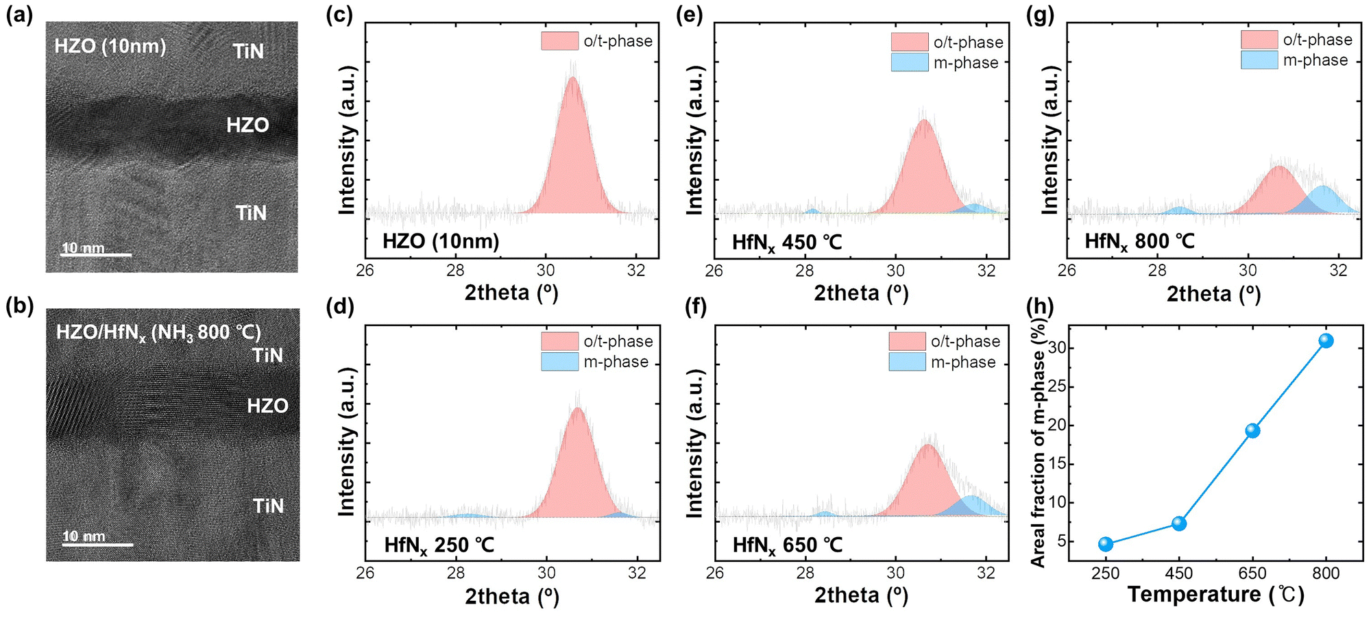 | ||
| Fig. 1 The cross-sectional HRTEM images of (a) TiN/10-nm-thick HZO/TiN and (b) TiN/9-nm-thick HZO/1-nm-thick HfNx films annealed in NH3 at 800 °C/TiN. Both samples were annealed at 450 °C in N2 gas for 30 seconds following the formation of the TE. Enlarged section (26–32.5°) of the GIXRD patterns, displaying the results for (c) the 10-nm-thick HZO sample and NH3-annealed HfNx (1-nm-thick) films at (d) 250 °C, (e) 450 °C, (f) 650 °C, and (g) 800 °C. The areas shaded in light red and light blue were identified as the o/t-phase and m-phase peaks, respectively, using Gaussian fitting. (h) Calculated m-phase areal fractions (%) corresponding to the conditions in (d) through (g). | ||
Fig. 1(c) shows the GIXRD pattern of the 10-nm-thick HZO film in the 2θ range with well-resolved o- and m-phase characteristic peaks. Fig. 1(d)–(g) show the GIXRD patterns of the 9-nm thick HZO/1-nm thick HfNx films, where the annealing temperature of HfNx IL was varied from 250 to 800 °C. All samples underwent a PMA process at 450 °C following the deposition of the TiN TE. To quantify these phase changes, GIXRD patterns between 2θ = 26° and 2θ = 32.5° were deconvoluted using the Gaussian function. Fig. S2(a) and (b) (ESI†) show the wide range θ–2θ GIXRD data and overlapped peaks in the narrow 2θ range. As the NH3 annealing temperature increased from 250 °C to 800 °C, the o/tetragonal (t)-phase peak at 2θ = 30.6° (indicated by the red background) diminished. In contrast, the m-phase peaks at 2θ = 28.5° and 2θ = 31.8° (indicated by the blue background) intensified. These trends suggest that the phase of the HZO film transformed from o/t-phase to m-phase as the IL annealing temperature increases. The m-phase fraction was determined using eqn (1):34
 | (1) |
The effect of the HfNx IL on the grain size of HZO film was investigated using scanning electron microscopy (SEM) analysis. Fig. 2(a) and (b) show the surface morphology of a 10-nm thick HZO and 9-nm thick HZO/1-nm thick HfNx film, where the HfNx IL was NH3 annealed at 800 °C. Both HZO films underwent RTA at 450 °C for 30 seconds to emulate the PMA condition without the TiN TE deposition. Depositing TiN TE and removing it after PMA is desirable for accurate grain size and phase identification. However, these steps damaged the top surface morphologies of the HZO layer, not allowing the appropriate SEM image acquisition. Nonetheless, the adopted experimental procedure could identify the grain size trend.
 | ||
| Fig. 2 SEM images and grain size analysis of HZO and TiN films with and without the HfNx layer. (a) SEM image of a 10-nm-thick HZO sample and (b) a 9-nm-thick HZO/1-nm-thick HfNx film annealed in NH3 at 800 °C. (c) Average grain diameter of the without and with HfNx samples annealed in NH3 at various temperatures. (d) SEM image of a 50-nm-thick TiN film and (e) a 50-nm-thick TiN film annealed in NH3 at 800 °C. (f) Average grain diameter corresponding to (d) and (e). (g) SEM image of a 10-nm-thick HfNx film on TiN and (h) a 10-nm-thick HfNx film annealed in NH3 at 800 °C on TiN. (i) Average grain diameter corresponding to (g) and (h). Grain size analysis in (c), (f), and (i) was performed using the watershed method in Gwyddion software. | ||
The 9-nm thick HZO/1-nm thick HfNx film exhibited larger grains (∼9.0 nm in average diameter) than the 10-nm-thick HZO film (∼7.1 nm). Fig. 2(c) shows the variation of HZO grain diameter as a function of IL RTA temperature. The results indicate that the HZO grain size increased with higher IL annealing temperatures. Previous studies reported that it influences the stabilization of the o-phase in FE HZO films by affecting surface energy.35–38 Smaller grain sizes stabilize the o-phase, which has lower surface energy than the m-phase.39,40Fig. 2(d) and (e) show the surface morphology of the TiN BE before and after NH3 RTA at 800 °C, respectively. Fig. 2(f) shows the quantitative data of the average TiN grain diameter, indicating an increase from ∼2.7 nm to ∼3.3 nm by RTA. Fig. 2(g) and (h) show the surface morphology of the 10-nm-thick HfNx film deposited on the TiN BE (the grain size of 1-nm-thickness was too thin to examine by SEM) before and after NH3 RTA at 800 °C, respectively. Fig. 2(i) shows the quantitative analysis of the grain radius, indicating an increase from ∼3.3 nm to ∼4.9 nm after annealing. Therefore, when NH3 RTA was applied to the HfNx/TiN layer, the increase in grain size was more pronounced than that observed for the TiN BE alone. This increased grain growth in the HfNx/TiN layer promoted the grain growth of the HZO film and increased the m-phase fraction, as shown in Fig. 1(h).
2.2. Chemical and interfacial properties of HZO films with NH3 annealing
Fig. 3 shows the variations in the film density (left y-axis) and roughness (right y-axis) of the 10-nm-thick HfNx film achieved by X-ray reflectivity (XRR) and atomic force microscopy (AFM) (again, the 1-nm thickness was too thin to obtain accurate data) after NH3 annealing at temperatures ranging from 250 °C to 800 °C. Fig. S3 (ESI†) shows the raw XRR and AFM data. The film density increased from ∼7.76 g cm−3 at 250 °C to ∼9.03 g cm−3 at 800 °C, corresponding to a 16% increase. This increase was attributed to the enhanced mobility of atoms at higher temperatures, which resulted in a denser atomic arrangement and decreased free volume within the film.41 Similarly, the surface roughness (Rq) increased from ∼0.31 nm at 250 °C to ∼0.73 nm at 800 °C. This increase was attributed to the grain growth and non-uniform nitrogen diffusion into the film surface, a characteristic effect of NH3 annealing.42,43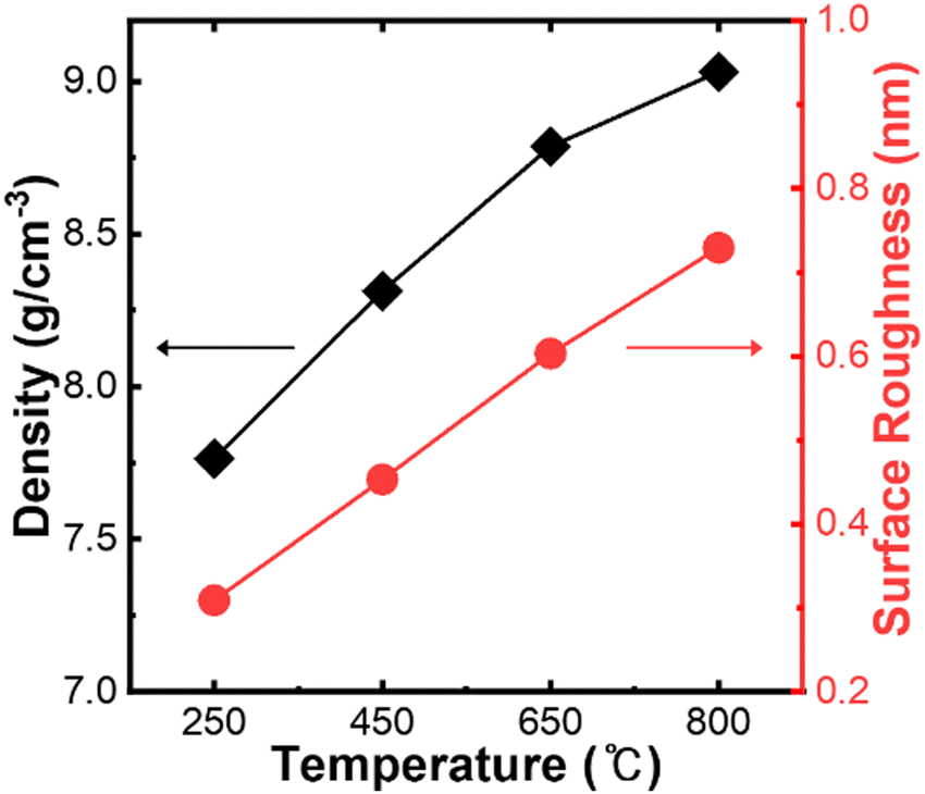 | ||
| Fig. 3 Summary of density and surface roughness of 10-nm-thick HfNx films annealed at NH3 temperatures (250 °C to 800 °C). | ||
Fig. 4(a) shows the deconvoluted X-ray photoelectron spectroscopy (XPS) Hf 4f spectrum of a TiN/5-nm-thick HZO/TiN stack after the PMA. The HZO layer thickness was decreased to 5 nm to improve the accuracy of nitrogen detection near the BE interface. The TiN TE was removed by wet-etching before the XPS analysis. The Hf–O bonds were observed at 18.7 eV and 17.0 eV binding energies, corresponding to 4f5/2 and 4f7/2, respectively. Fig. 4(b) shows the deconvoluted XPS Hf 4f spectra of the TiN/5-nm-thick HZO/1-nm-thick HfNx/TiN stack when the NH3 annealing was performed at 250 °C after depositing the HfNx IL. A decrease in the intensity of Hf–O bonds was observed (blue line), along with the appearance of Hf–N bond peaks at 17.8 eV and 16.9 eV (green line).44–47Fig. 4(c) shows the deconvoluted XPS Hf 4f spectra of the TiN/5-nm-thick HZO/1-nm-thick HfNx/TiN stack when the NH3 annealing was performed at 800 °C after depositing the HfNx IL. The increase in Hf–N bonding was more pronounced in this case than in others. The XPS results indicated that increasing the NH3 annealing temperature of the HfNx IL enhanced nitrogen incorporation into the HZO. Fig. S4 (ESI†) shows the proposed mechanism based on these findings. As the NH3 annealing temperature increased from 250 °C to 800 °C, the oxygen concentration at the HfNx surface decreased while the nitrogen concentration increased. During the subsequent HZO deposition and PMA processes, the diffused nitrogen facilitated the formation of Hf–N (or O–N) bonds and filled the oxygen vacancies (Vo) with nitrogen ions. The increased nitrogen concentration may also suppress the diffusion of Vo within the HZO layer.48
 | ||
| Fig. 4 Deconvoluted XPS Hf 4f spectrum of (a) a 5-nm-thick HZO film, and 5-nm-thick HZO/1-nm-thick HfNx films annealed in NH3 at (b) 250 °C and (c) 800 °C. | ||
2.3. Electrical performance and reliability of HZO films with and without a 1-nm-thick HfNx interfacial layer
Fig. 5(a) shows the polarization–electric field (P–E) hysteresis curves, measured by the positive-up-negative-down (PUND) test with two triangular positive pulses and two triangular negative pulses (±3.5 MV cm−1), of TiN/10-nm thick HZO/TiN and TiN/9-nm-thick HZO/1-nm-thick HfNx/TiN capacitors, where the 1-nm-thick HfNx IL underwent NH3 RTA at temperatures ranging from 250 °C to 800 °C. The results indicated that the 10-nm-thick HZO sample exhibited the highest Pr value, while samples with the HfNx IL showed gradually decreasing Pr with increasing NH3 annealing temperature with the lowest Pr value when annealed at 800 °C. Fig. 5(b) shows the variation in 2Pr and 2Ec values derived from the P–E hysteresis curves in Fig. 5(a). The sample with no IL exhibited a 2Pr value of 29.34 μC cm−2, while samples with the 1-nm-thick HfNx IL showed a decrease in 2Pr with increasing NH3 annealing temperature. Specifically, the 2Pr value decreased from 27.5 μC cm−2 at 250 °C to 4.07 μC cm−2 at 800 °C. Notably, the 2Ec values slightly increased from 2.49 MV cm−1 at 250 °C to 2.68 MV cm−1 at 800 °C. These results deviate from the proportional relationship between Pr and Ec commonly observed in HfO2-based films.49 The decrease in Pr was attributed to the increased m-phase fraction within the HZO film, as indicated by the GIXRD results in Fig. 1(h), due to the promoted nitrogen diffusion and enhanced grain growth. The structural changes also affected the dielectric constant (εr), as shown in Fig. S5 (ESI†). Samples with HfNx IL annealed in NH3 exhibited a lower εr (∼26 at 800 °C) than the 10-nm thick HZO sample (∼46). The observed decrease in εr was consistent with an increased m-phase fraction, further supporting the structural changes revealed by GIXRD in Fig. 1(h) and Fig. S2 (ESI†). Suppose the increased m-phase grains form a serially connected configuration with the o-phase grains along the out-of-plane direction. In that case, the Pr value must remain unvaried (or slightly increased), but the Ec value must be increased due to the tunnel-switch effect of the non-FE m-phase layer.50 Therefore, the o/t-phase and m-phase most probably form a parallel configuration, and the FE o-phase property solely determines the Ec value. DFT calculation was performed to understand this effect, assuming that nitrogen incorporation increased the FE switching barrier in the HZO layer. | ||
| Fig. 5 (a) P–E curves of the TiN/10-nm-thick HZO/TiN sample and TiN/9-nm-thick HZO/1-nm-thick HfNx/TiN films annealed in NH3 at temperatures ranging from 250 °C to 800 °C. Measurements were conducted on MFM capacitors using the PUND method. (b) Summary of 2Pr and 2Ec values derived from the PUND measurements in (a). (c) P–E curves of TiN/10-nm-thick HZO/P++Si and TiN/9-nm-thick HZO/1-nm-thick HfNx/P++Si MFIS capacitors were measured using the PUND method. (d) Summary of 2Pr and 2Ec values obtained from the PUND curves in (c). (e) Pr and Ec behavior results of HZO thin films with NH3-annealed HfNx IL and HfO2 thin films with various dopants (Si, Y, Zr). The data for Si, Y, and Zr-doped films were taken from ref. 51–56. | ||
The DFT calculation evaluated the homogeneous switching barrier of a 2 × 2 × 2 HfO2 supercell containing a single oxygen vacancy coordinated with three Hf atoms (Vo3). The result was then compared to a similar structure where the Vo3 was replaced by nitrogen, forming a vacancy substitution coordinated with three Hf atoms (No3). Fig. S6 (ESI†) shows the DFT calculation results, demonstrating that No3 increased the activation energy (Ea) of the switching barrier compared to Vo3. The calculated Ea for No3 was 4.16 eV per cell, higher than the 3.96 eV per cell for Vo3. This increase in Ea was attributed to the structural changes induced by nitrogen incorporation. A Vo3 created additional free space within the lattice, facilitating polarization switching by allowing easier movement.
In contrast, when the No3 filled Vo3, the lattice became more constrained, making polarization switching sluggish. As a result, a higher electric field was required to overcome the barrier, and thus, a higher Ec must be induced. Therefore, the appropriate incorporation of nitrogen into the 9-nm-thick HZO film through the chemical interaction with the nitrogen-containing HfNx IL decreases the Pr by forming parallel m-phase grains, while the Ec of the remaining o-phase slightly increases due to the higher switching barrier. It should be noted that the Ec of parallel m- and o-phase is solely determined by the FE o-phase. This finding corresponds to the desirable direction of the FeTFT device, as discussed above.
Fig. 5(c) shows the P–E hysteresis curves using PUND pulses of the MFIS capacitors with the TiN/10-nm-thick HZO/P++Si and TiN/9-nm-thick HZO/1-nm-thick HfNx/P++Si structures described in Fig. S1(b) (ESI†). The measurements were performed at a 3.5 MV cm−1 bias field strength and 1 kHz frequency, similar to the conditions used for the MFM case. The MFIS with no IL showed the highest Pr value, while samples with the HfNx IL showed a gradual decrease in Pr with increasing NH3 annealing temperature. This trend was consistent with the behavior observed for the MFM capacitors. Fig. 5(d) shows the variation in 2Pr and 2Ec values derived from the PUND P–E hysteresis curves in Fig. 5(c). The sample with no IL exhibited a 2Pr value of 39.9 μC cm−2. For samples with the 1-nm-thick HfNx IL, the 2Pr value decreased from 32.8 μC cm−2 at 250 °C to 5.8 μC cm−2 at 800 °C. In contrast, the 2Ec values slightly increased from 8.45 MV cm−1 for the no IL sample to 9.45 MV cm−1 for the sample annealed at 800 °C. The estimated Ec values were higher for the samples on the P++Si substrate than on the TiN substrate. This increase in Ec was attributed to the charge injection caused by the tunneling switch effect of the native oxide layer on the Si surface and partaking of the voltage by the finite accumulation and depletion layer thicknesses of the Si substrate.21
Fig. 5(e) shows the relationship between Pr and Ec for various doped-HfO2 films in MFM configurations reported in the literature, including experimental data from this study. Si,51,52 Y,53,54 and Zr-doped HfO2 films55,56 from other works exhibited a proportional relationship between Pr and Ec. In contrast, the samples with the NH3-annealed HfNx IL showed an unusual inverse Prvs. Ec relationship (star symbols). This result demonstrated that Pr could be controlled independently of Ec, a behavior not typically observed in conventional FE materials.
Fig. 6(a) shows the endurance performance of the various MFM capacitors with a cycling electric field of 3.5 MV cm−1 at 100 kHz. Samples with the HfNx IL showed stable endurance beyond 107 cycles, while the single-layer HZO sample exhibited a hard breakdown before 107 cycles. The improved endurance of the samples with HfNx IL was attributed to the reduction in Pr and the decreased oxidation of the TiN BE. As Pr decreased, the charge displacement during polarization switching was decreased, thereby minimizing charge-induced defect formation within the HZO layer during cycling.57,58 Simultaneously, the HfNx IL suppressed the formation of interfacial oxides (TiOx or TiOxNy) on the TiN BE.32 As the NH3 annealing temperature increased, nitrogen diffusion into the HZO layer further promoted m-phase formation, as shown in Fig. 1(h), contributing to Pr reduction and suppressing the adverse interfacial reaction. These combined effects further enhanced the endurance performance. Fig. 6(b) shows the variation in 2Ec under cycling conditions at 3.5 MV cm−1. The samples with HfNx IL exhibited stable 2Ec values regardless of cycling, consistent with the trends observed in Fig. 6. These results demonstrated that nitrogen incorporation was crucial for maintaining Ec values.
 | ||
| Fig. 6 Endurance test results of TiN/10-nm-thick HZO/TiN and TiN/9-nm-thick HZO/1-nm-thick HfNx/TiN films annealed in NH3 at 250 °C to 800 °C/TiN for the cycling field strengths of (a) 3.5 MV cm−1 at the frequency of 100 kHz. (b) 2Ec values of endurance by NH3 annealing temperature in (a). (c) J–E characteristics of the sample with no IL and TiN/9-nm-thick HZO/1-nm-thick HfNx/TiN films annealed in NH3 at 250 °C to 800 °C. | ||
Fig. 6(c) shows the characteristics of the current density–electric field (J–E). The leakage current was significantly decreased in the samples with the HfNx IL compared to the no IL sample. The sample with the HfNx IL annealed at 800 °C in NH3 recorded the lowest leakage current (∼3.7 × 10⁻⁸ A cm−2 at 2.0 MV cm−1), while the no IL sample exhibited a much higher leakage current (∼1.5 × 10⁻⁵ A cm−2 at 2.0 MV cm−1). Without the HfNx IL, the TiN electrode likely forms interfacial oxides, such as TiOx or TiOxNy, by taking oxygen atoms from the HZO layer. These oxides negatively impacted the TiN/HZO interface, and the induced Vo in the HZO layer degraded the FE reliability of the HZO film. This observation was consistent with the findings reported by Kim et al.32 Overall, the NH3 annealing diminished the adverse interfacial reaction and improved the film performance.
2.4. Improved memory performance of a-IGZO channel FeTFTs through an HfNx interfacial layer and NH3 annealing
After the 1-nm-thick HfNx IL was deposited and NH3 annealing was performed, the Pr of the HZO layer was found to decrease while Ec slightly increased, as discussed in Section 3.3. Park et al. previously reported that achieving an optimal Pr was essential for retaining the threshold voltage (Vth) shift or MW close to 2Vc.19 The results in the previous section indicate that HZO films with an HfNx IL can be more suitable for FeTFT structures, although they are less desirable for MFM capacitor applications. Fig. S1(c) (ESI†) shows a schematic diagram of the a-IGZO FeTFT fabrication, incorporating HfNx IL and HZO layers on a P++Si bottom gate (G). In the operational behavior of a-IGZO FeTFTs, the n-type nature of a-IGZO was found to limit the electric field distribution within the channel. In program mode, the P++Si gate was positively biased, and the accumulated electrons in the a-IGZO layer fluently compensated for the positive FE-bound charge at the HZO/a-IGZO interface, turning the channel on, resulting in a low Vth. Conversely, the P++Si gate was negatively biased in erase mode, and the negative FE-bound charge must be located near the HZO/a-IGZO interface. However, the limited hole generation in the n-type a-IGZO inversion charges could not fluently compensate for the negative FE-bound charge. Instead, Vo and the laterally spreading electric field from the source and drain (S and D) electrodes compensated the negative FE-bound charge.59Fig. 7(a)–(e) shows the transfer characteristics of a-IGZO FeTFTs, presenting the drain current–gate voltage (ID–VG) on the left y-axis and transconductance (gm) on the right y-axis as functions of VG. The FE gate stack consists of (a) a 10-nm-thick HZO and (b)–(e) a 9-nm-thick HZO film deposited on a 1-nm-thick HfNx IL, annealed at 250, 450, 650, and 800 °C, respectively, in an NH3 atmosphere. All FeTFT devices exhibited ID–VG curves with counterclockwise hysteresis, coinciding with the FE switching, except for the sample annealed at 800 °C. The VG sweep range was set to −4.5 V to +4.5 V for the sample in (a) and −5.5 V to +5.5 V for the other samples because the sample in (a) showed breakdown at voltages exceeding 4.5 V.
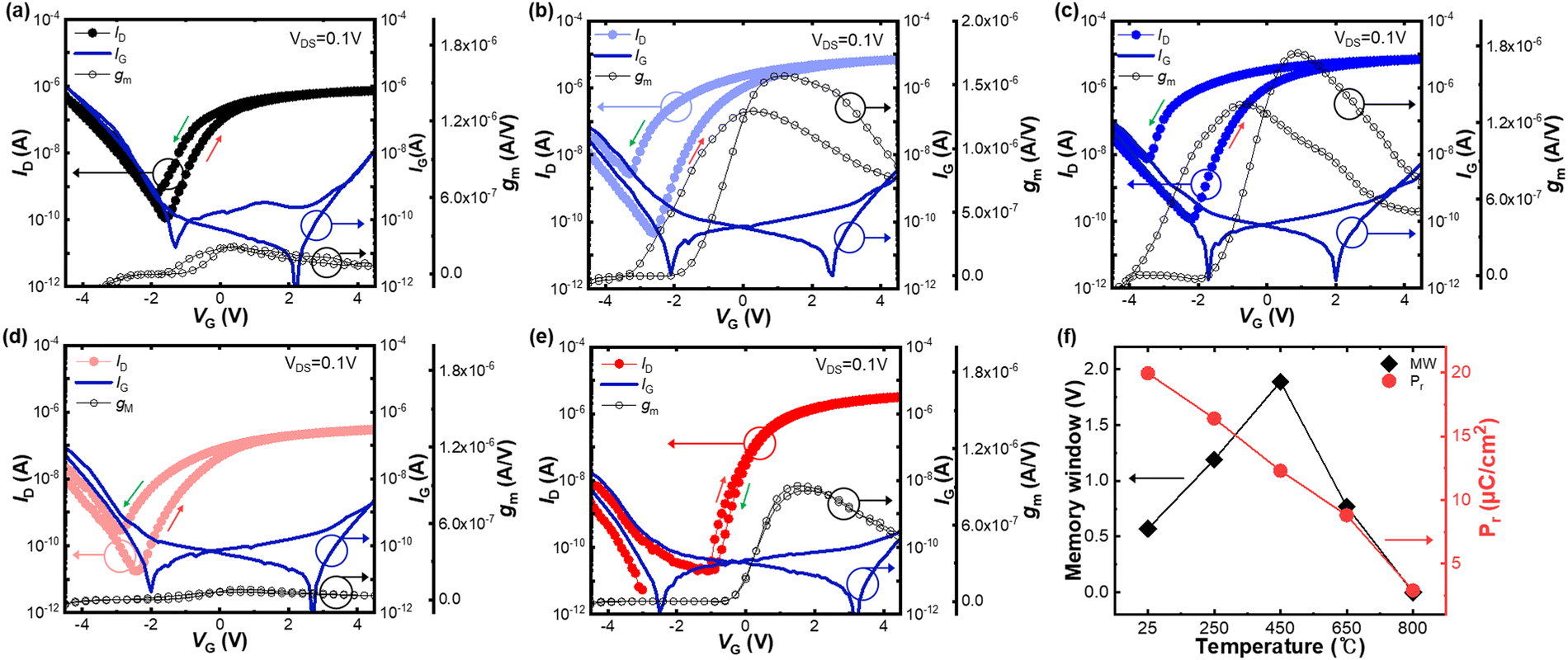 | ||
| Fig. 7 Transfer curve (ID–VG, IG–VG, and gm–VG) of the a-IGZO TFTs with ferroelectric HZO. (a) 10-nm-thick HZO, and (b)–(e) 9-nm-thick HZO film deposited on a 1-nm-thick HfNx IL annealed in NH3 at (b) 250 °C, (c) 450 °C, (d) 650 °C, and (e) 800 °C. (f) Summary of MW and Pr values for the 10-nm-thick HZO sample and with 1-nm-thick HfNx IL at NH3 annealing temperatures (250–800 °C). | ||
The MW of the HZO films in the a-IGZO FeTFT structure was determined from the ID–VG curves measured during forward and backward voltage sweeps.60 First, the gm was derived from the ID–VG curves by differentiating the ID for the VG, following eqn (2). The maximum transconductance value (gm,max) was determined during the forward and backward sweeps, and the corresponding gate voltages for these maxima were determined: Vfwdgm,max for the forward sweep and Vbwdgm,max for the backward sweep. At each Vgm,max point, a tangent line on the ID–VG curves was used to determine the x-intercept, accurately representing the voltage shift. Finally, MW was calculated as the difference between the x-intercepts (Vx-int) of the forward and backward sweeps, as shown in eqn (3):
| gm = ∂ID/∂VG | (2) |
| Memory window (MW) = Vfwdx-int − Vbwdx-int | (3) |
The calculated MW of the sample without the IL was 0.57 V. In contrast, the MW values for the samples with the 1-nm-thick HfNx IL varied with the NH3 annealing temperature. The MW increased to 1.19 V at 250 °C to a peak value of 1.89 V at 450 °C, then decreased to 0.77 V at 650 °C. At 800 °C, a charge-trap-like phenomenon (clockwise hysteresis) was observed. Besides, the gate leakage current (IG)–VG curves (navy lines) showed a butterfly shape, confirming the FE nature of the gate insulator stack,61,62 with the sample containing 1-nm-thick HfNx IL exhibiting lower IG, indicating the lowest defect concentration. This behavior is consistent with the leakage observed in the MFM structure shown in Fig. 6(c). The high ID observed in the highly negative bias region coincided with the IG, indicating that it is not due to the ambipolar conduction behavior of the a-IGZO channel.
Fig. 7(f) shows the relationship between MW and Pr (reproduced from Fig. 5(d)) for the a-IGZO FeTFTs. From no IL device to the device with IL annealed at 450 °C, the MW increases while Pr decreases. This behavior could be ascribed to the decreased depolarization effect of the FE film with lower Pr as the IL annealing temperature increased to 450 °C. However, further increasing the IL annealing temperature decayed the Pr to below ∼10 μC cm−2, which again decreased the MW due to too small Pr.
Still, the MW of the a-IGZO TFT structure was observed to be smaller than 2Vc even at the optimized condition. This reduction was attributed to ineffective charge compensation at the FE/a-IGZO interface. The n-type nature of a-IGZO limited the availability of inversion charges, leading to incomplete polarization switching, thereby reducing the MW.20,21 A summary of the MW, leakage current, and endurance characteristics is provided in Table 1 for comparison.
| Sample | Memory window (V) | Leakage current (A cm−2) | Endurance (cycles) |
|---|---|---|---|
| 10-nm-thick HZO (without HfNx) | 0.57 | ∼1.5 × 10⁻⁵ | 106 |
| HfNx 250 °C | 1.19 | ∼7.0 × 10⁻⁶ | >107 |
| HfNx 450 °C | 1.89 | ∼3.6 × 10⁻⁶ | >107 |
| HfNx 650 °C | 0.77 | ∼1.2 × 10⁻⁶ | >107 |
| HfNx 800 °C | 0 | ∼3.7 × 10⁻⁸ | >107 |
Fig. 8 shows the room-temperature retention characteristics of the FeTFT with (a) no IL and (b)–(d) with IL annealed at temperatures of 250 °C, 450 °C, and 650 °C, respectively. Retention measurements were not performed for the 800 °C sample due to the absence of a measurable MW. The MW of the sample in (a) was expected to last less than one year, while the MW of the HfNx IL sample was expected to last longer. Among them, the sample annealed at 450 °C demonstrated the most stable retention, with the predicted MW of ∼1.0 V maintained after 10 years. These results demonstrated that NH3 annealing at 450 °C minimized charge trapping, enabling the FeTFT device to ensure reliable and stable data storage over extended periods, which is crucial for nonvolatile memory applications.
 | ||
| Fig. 8 Data retention characteristics of (a) HZO-based IGZO FeTFTs (10-nm-thick HZO layer) and devices incorporating 1-nm-thick HfNx IL annealed in NH3 at (b) 250 °C, (c) 450 °C, and (d) 650 °C. | ||
3. Experimental sections
A 50-nm-thick TiN BE was deposited on a 100-nm-thick SiO2/Si substrate using DC sputtering (ENDURA 5500, Applied Materials, USA). Subsequently, a 1-nm-thick HfNx IL was deposited on the TiN/SiO2/Si substrate using thermal ALD (Atomic-Classic, CN-1) with tetrakis-ethylmethylaminohafnium (Hf[N(C2H5)CH3]4, TEMA-Hf) as the Hf precursor and NH3 gas as the N-source, following the specific chamber purge conditions mentioned above.31 The bubbler-type TEMA-Hf canister and gas line were maintained at 65 °C and 100 °C, respectively. The precursor was carried by the Ar carrier gas at a flow rate of 950 standard cubic centimeters per minute (sccm), which was also used as the purge gas. The flow rate of NH3 gas was 50 sccm. The optimized ALD sequence was TEMA-Hf pulse (5 s) – Ar purge (60 s) – NH3 pulse (0.5 s) – Ar purge (60 s), which was repeated for 10 cycles to grow a 1-nm-thick HfNx film. The HfNx films were post-deposition annealed in an NH3 atmosphere using a rapid thermal process (RTP, Real RTP-100, ULTECH) at temperatures ranging from 250 to 800 °C for 60 s. Annealing for 30 s under similar conditions was insufficient for improving the ferroelectric performances. After the RTP, all HZO films were deposited using another thermal ALD system (Atomic-Classic, CN-1) at a substrate temperature of 280 °C. To ensure a consistent total thickness across all samples, the HfNx inserted samples were fabricated with a 1-nm-thick HfNx IL and a 9-nm-thick HZO layer. In contrast, the sample without HfNx used a 10-nm-thick HZO layer. The total stack thickness was maintained at 10 nm for all samples. TEMA-Hf and tetrakis-ethylmethylaminozirconium (Zr[N(C2H5)CH3]4, TEMA-Zr) were used as Hf- and Zr-precursors, respectively, and O3 (180 g m−3 density) as the oxygen source. The ALD sequence was TEMA-Hf, Zr pulse (0.8, 1.4 s) – Ar purge (30 s) – O3 pulse (5 s) – Ar purge (10 s). For the electrical characterization, a 50-nm-thick TiN TE was deposited at room temperature using RF sputtering (SRN-120, SORONA Inc.). During the TE deposition process, a shadow mask with an opening diameter of ∼300 μm was used for defining the capacitor area. After fabricating the TiN/HZO/HfNx/TiN capacitors, the PMA process was conducted at 450 °C for 30 s in an N2 atmosphere at 110 Torr to crystallize the HZO film. Also, a P++Si substrate with a resistivity of less than 0.005 Ω cm was employed as the BE in the MFIS structure, replacing the TiN BE. The same deposition procedures were followed for MFIS sample fabrication. The FeTFT also adopted the P++Si substrate as the bottom gate material.To fabricate FeTFTs, 1-nm-thick HfNx IL was deposited on the P++Si bottom gate and NH3-annealed at temperatures from 250 °C to 800 °C, followed by 9-nm-thick HZO thin film deposition. Then, a 20-nm-thick a-IGZO layer was deposited on the HZO at room temperature using RF magnetron sputtering (SRN-120, SORONA Inc.). The films were annealed at 400 °C for 30 s in an N2 atmosphere via RTA to crystallize the HZO layer. Subsequently, a 50 nm-thick TiN film was deposited using RF sputtering (SRN-120, SORONA Inc.), and TiN source/drain electrodes were patterned to achieve a Wch of 20 μm and a Lch of 5 μm. The PMA was performed at 350 °C in a furnace to enhance contact with the a-IGZO channel and repair deposition-induced damage. Fig. S1 (ESI†) shows the schematic diagram of the fabrication steps for FE HZO devices on TiN thin-film electrodes and P++Si substrates.
The film compositions were measured using X-ray fluorescence (XRF, Quant'X, Thermo SCIENTIFIC), and the microstructure of the fabricated samples was analyzed using HRTEM (JEM-2100F, JEOL). The crystallinity and phases of the HfNx and HZO thin films were analyzed using GIXRD (X'pert Pro, PANalytical) with an angle of incidence = 0.5°. Bulk film density was estimated using XRR (X'pert Pro, PANalytical). The chemical bonding states and composition of the HfNx and HZO films were evaluated using XPS (Versaprobe III, PHI). The topography and grain configuration of the films were analyzed using AFM (NX10, Park Systems) and SEM (SIGMA, Carl Zeiss). The grain sizes of the HZO and HfNx films were quantified and statistically analyzed from plane-view SEM images using the watershed method in Gwyddion software.
DFT calculations were carried out using the Vienna Ab initio Simulation Package,63,64 applying the local density approximation65,66 combined with Blöchl's projector augmented wave method.67,68 A plane-wave energy cutoff of 600 eV was employed, and Γ-centered k-point meshes of 4 × 4 × 4 were used for the 2 × 2 × 2 supercells of orthorhombic HfO2. The atomic positions were relaxed until the Hellmann–Feynman forces were reduced to below 0.02 eV Å−1. The energy barrier for switching was determined using the nudged elastic band method with fixed lattice constants for the 2 × 2 × 2 supercells.69
For electrical characterization, P–E curves were measured using a ferroelectric tester (TF Analyzer 2000, Aixacct system) with a triangular bipolar pulse at 1 kHz. PUND tests were also performed to extract accurate Pr values free from leakage current interference. All P–E curve results were obtained after wakeup (cycling of 105 with an amplitude of 3.5 MV cm−1 at a frequency of 100 kHz). J–E characteristics of the HZO films were evaluated using a picoammeter (HP4140D, Hewlett Packard). Additionally, a semiconductor parameter analyzer (SPA, 4145B, Hewlett Packard) was used to measure the ID–VG, IG–VG, and retention characteristics of the FeTFTs.
4. Conclusions
This study investigated the effects of ALD HfNx IL insertion and NH3 annealing on the properties of the HZO-film-based MFM and MFIS capacitors and FeTFTs with an a-IGZO channel. A 1-nm-thick HfNx IL was adopted for the capacitor structures between the 9-nm-thick HZO film and BEs (TiN or P++Si). The 2Pr values of the HZO were observed to decrease with increasing NH3 annealing temperatures, while the 2Ec values slightly increased. The decreased 2Pr could be ascribed to the increased m-phase fraction due to the larger grain size of the HZO film when it was grown on high-temperature annealed HfNx IL. The 2Ec values are solely determined by the o-phase grains in the film, and the nitrogen diffusion into the HZO film increased the switching barrier of the o-phase HZO. DFT calculation supported this conclusion.The FeTFT with no IL showed inappropriate MW (∼0.57 V) and retention performance (<1 year) due to too high Pr (invoking a strong depolarization effect) and high leakage current of the HZO film. In contrast, the 450 °C NH3 annealing condition for the 1-nm-thick HfNx IL was confirmed to achieve the highest MW of ∼1.89 V in FeTFT devices. The appropriate incorporation of the nitrogen enhanced the resistance to performance degradation by charge injection, meaning that the MW of ∼1.0 V was retained for up to 10 years. Other conditions with higher Pr, due to high depolarization, and lower Pr, due to too low bound charge effect, degraded the MW and retention performances.
Therefore, interposing the 1-nm-thick HfNx IL and NH3 annealing at 450 °C was a feasible method to enhance the FE and memory performance of a-IGZO FeTFTs. This study provides a notable strategy to decouple the Pr and Ec, which is usually unachievable in conventional FE film technology.
Author contributions
H. W. Nam designed and conducted the experiments and wrote the manuscript. J. H. Lee, S. J. Shin, K. D. Kim, S. K. Ryoo, and K. H. Ye helped plan the experiments and analyze data. S. Y. Byun, I. S. Lee, S. H. Lee, J. H. Song and J. H. Choi reviewed the manuscript. C. S. Hwang supervised the whole research experiments and manuscript preparation.Data availability
The data supporting this article have been included as part of the ESI.† The data that support the findings of this study are available from the corresponding author upon reasonable request.Conflicts of interest
The authors declare they have no conflict of interest.Acknowledgements
This work was supported by the National Research Foundation of Korea (no. 2020R1A3B2079882).Notes and references
- K. Florent, M. Pesic, A. Subirats, K. Banerjee, S. Lavizzari, A. Arreghini, L. Di Piazza, G. Potoms, F. Sebaai and S. McMitchell. In 2018 IEEE Int. Electron Devices Meet., 2018, pp. 2–5.
- J. Müller, E. Yurchuk, T. Schlösser, J. Paul, R. Hoffmann, S. Müller, D. Martin, S. Slesazeck, P. Polakowski and J. Sundqvist, In 2012 Symp. VLSI Technol., 2012, pp. 25–26.
- S. Dünkel, M. Trentzsch, R. Richter, P. Moll, C. Fuchs, O. Gehring, M. Majer, S. Wittek, B. Müller and T. Melde, In 2017 IEEE Int. Electron Devices Meet., 2017, pp. 19–27.
- M. H. Park, H. J. Kim, Y. J. Kim, W. Jeon, T. Moon and C. S. Hwang, Phys. Status Solidi RRL, 2014, 8, 532–535 CrossRef CAS.
- M. Pešić, S. Knebel, K. Cho, C. Jung, J. Chang, H. Lim, N. Kolomiiets, V. V. Afanas'ev, T. Mikolajick and U. Schroeder, Solid-State Electron., 2016, 115, 133–139 CrossRef.
- W. Weinreich, A. Shariq, K. Seidel, J. Sundqvist, A. Paskaleva, M. Lemberger and A. J. Bauer, J. Vac. Sci. Technol., B: Nanotechnol. Microelectron.: Mater., Process., Meas., Phenom., 2013, 31, 01A109 Search PubMed.
- M. K. Kim and J. S. Lee, Nano Lett., 2019, 19, 2044–2050 CrossRef CAS PubMed.
- Y. Kato, Y. Kaneko, H. Tanaka and Y. Shimada, Jpn. J. Appl. Phys., 2008, 47, 2719–2724 CrossRef CAS.
- D. Kim, Y. R. Jeon, B. Ku, C. Chung, T. H. Kim, S. Yang, U. Won, T. Jeong and C. Choi, ACS Appl. Mater. Interfaces, 2021, 13, 52743–52753 CrossRef CAS PubMed.
- F. Mo, Y. Tagawa, C. Jin, M. Ahn, T. Saraya, T. Hiramoto and M. Kobayashi, IEEE J. Electron Devices Soc., 2020, 8, 717–723 CAS.
- F. Mo, T. Saraya, T. Hiramoto and M. Kobayashi, Appl. Phys. Express, 2020, 13, 074005 CrossRef CAS.
- S. Miller and P. McWhorter, J. Appl. Phys., 1992, 72, 5999–6010 CrossRef CAS.
- F. Preisach, Über die Magnetische Nachwirkung, Z. Med. Phys., 1935, 94, 277–302 Search PubMed.
- T. Kamei, E. Tokumitsu and H. Ishiwara, Trans. Inst. Electron., Inf. Commun. Eng., Sect. E, 1998, 81, 577–583 Search PubMed.
- H. T. Lue, C. J. Wu and T. Y. Tseng, IEEE Trans. Electron Devices, 2002, 49, 1790–1798 CrossRef.
- J. M. Sallese and V. Meyer, IEEE Trans. Electron Devices, 2004, 51, 2145–2153 CrossRef CAS.
- T. Ma and J. P. Han, IEEE Electron Device Lett., 2002, 23, 386–388 CAS.
- C. Black, C. Farrell and T. J. Licata, Appl. Phys. Lett., 1997, 71, 2041–2043 CrossRef CAS.
- H. W. Park, J. G. Lee and C. S. Hwang, Nano Select, 2021, 2, 1187–1207 CrossRef CAS.
- T. Ando, Materials, 2012, 5, 478–500 CrossRef CAS PubMed.
- J. H. Lee, Y. Lee, J. K. Han, K. D. Kim, S. R. Byun, H. W. Park and C. S. Hwang, Adv. Electron. Mater., 2024, 2400516 Search PubMed.
- S. Fichtner, N. Wolff, F. Lofink, L. Kienle and B. Wagner, J. Appl. Phys., 2019, 125, 114103 CrossRef.
- D. Drury, K. Yazawa, A. Zakutayev, B. Hanrahan and G. Brennecka, Micromachines, 2022, 13, 887 Search PubMed.
- S. K. Ryoo, K. D. Kim, H. W. Park, Y. B. Lee, S. H. Lee, I. S. Lee, S. Byun, D. Shim, J. H. Lee and H. Kim, Adv. Electron. Mater., 2022, 8, 2200726 Search PubMed.
- K. D. Kim, S. K. Ryoo, H. S. Park, S. Choi, T. W. Park, M. K. Yeom and C. S. Hwang, J. Appl. Phys., 2024, 136, 024101 Search PubMed.
- J. G. Scott and C. A. PazDeAraujo, Science, 1989, 246, 1400–1405 Search PubMed.
- H. R. Kim, S. H. Jeong, C. B. Jeon, O. S. Kwon, C. S. Hwang, Y. K. Han, D. Y. Yang and K. Y. Oh, J. Mater. Res., 2001, 16, 3583–3591 CrossRef CAS.
- J. Müller, T. Böscke, D. Bräuhaus, U. Schröder, U. Böttger, J. Sundqvist, P. Kücher, T. Mikolajick and L. Frey, Appl. Phys. Lett., 2011, 99, 112901 CrossRef.
- M. H. Park, Y. H. Lee, H. J. Kim, T. Schenk, W. Lee, W. Do, K. Kim, F. P. Fengler, T. Mikolajick, U. Schroeder and C. S. Hwang, Nanoscale, 2017, 9, 9973–9986 Search PubMed.
- M. H. Park, Y. H. Lee, H. J. Kim, Y. J. Kim, T. Moon, K. D. Kim, S. D. Hyun and C. S. Hwang, ACS Appl. Mater. Interfaces, 2018, 10, 42666–42673 CrossRef CAS PubMed.
- S. K. Ryoo, B. Y. Kim, Y. B. Lee, H. W. Park, S. H. Lee, M. Oh, I. S. Lee, S. Y. Byun, D. S. Shim and J. H. Lee, J. Mater. Chem. C, 2023, 11, 8018–8026 RSC.
- B. Y. Kim, H. W. Park, S. D. Hyun, Y. B. Lee, S. H. Lee, M. Oh, S. K. Ryoo, I. S. Lee, S. Byun and D. Shim, Adv. Electron. Mater., 2022, 8, 2100042 Search PubMed.
- B. Y. Kim, S. H. Kim, H. W. Park, Y. B. Lee, S. H. Lee, M. Oh, S. K. Ryoo, I. S. Lee, S. Byun and D. Shim, Appl. Phys. Lett., 2021, 119, 122902 Search PubMed.
- M. H. Park, J. H. Kim, Y. J. Kim, W. Lee, T. Moon and C. S. Hwang, Appl. Phys. Lett., 2013, 102, 242905 Search PubMed.
- K. Ishikawa, K. Yoshikawa and N. Okada, Phys. Rev. B: Condens. Matter Mater. Phys., 1988, 37, 5852–5856 CrossRef CAS PubMed.
- K. Nanda, A. Maisels, F. Kruis, H. Fissan and S. Stappert, Phys. Rev. Lett., 2003, 91, 106102 CrossRef CAS PubMed.
- F. D. Fischer, T. Waitz, D. Vollath and N. K. Simha, Prog. Mater. Sci., 2008, 53, 481–527 CrossRef CAS.
- B. Medasani, Y. H. Park and I. Vasiliev, Phys. Rev. B: Condens. Matter Mater. Phys., 2007, 75, 235436 CrossRef.
- C. Xu, Y. Song, L. Lu, C. Cheng, D. Liu, X. Fang, X. Chen, X. Zhu and D. Li, Nanoscale Res. Lett., 2013, 8, 1–7 CrossRef PubMed.
- S. Turteltaub and A. Suiker, Int. J. Solids Struct., 2006, 43, 7322–7336 Search PubMed.
- J. Thakur, R. Naik, V. Naik, D. Haddad, G. Auner, H. Lu and W. Schaff, J. Appl. Phys., 2006, 99, 023504 CrossRef.
- H. Hopoğlu, H. Aydınoğlu, A. Özer and E. Ş. Tüzemen, Opt. Mater., 2021, 122, 111685 CrossRef.
- D. Dastan, K. Shan, A. Jafari, F. Gity, X. T. Yin, Z. Shi, N. D. Alharbi, B. A. Reshi, W. Fu and Ş. Ţălu, Appl. Phys. A: Mater. Sci. Process., 2022, 128, 400 CrossRef CAS.
- S. Karwal, M. Verheijen, B. Williams, T. Faraz, W. Kessels and M. Creatore, J. Mater. Chem. C, 2018, 6, 3917–3926 RSC.
- A. Perry, L. Schlapbach and W. Sproul, Solid State Commun., 1987, 62, 23–26 CrossRef CAS.
- A. Arranz and C. Palacio, Surf. Sci. Spectra, 2004, 11, 33–42 CrossRef CAS PubMed.
- W. Wang, T. Nabatame and Y. Shimogaki, Surf. Sci., 2005, 588, 108–116 CrossRef CAS.
- D. R. Hsieh, C. C. Lee and T. S. Chao, IEEE Trans. Electron Devices, 2022, 69, 2074–2079 CAS.
- J. D. Anderson, J. Merkel, D. Macmahon and S. K. Kurinec, IEEE J. Electron Devices Soc., 2018, 6, 525–534 CAS.
- Q. Jiang, H. J. Lee, G. H. Kim and C. S. Hwang, Adv. Mater., 2009, 21, 2870–2875 CrossRef.
- P. D. Lomenzo, P. Zhao, Q. Takmeel, S. Moghaddam, T. Nishida, M. Nelson, C. M. Fancher, E. D. Grimley, X. Sang and J. M. LeBeau, J. Vac. Sci. Technol., B: Nanotechnol. Microelectron.: Mater., Process., Meas., Phenom., 2014, 32, 03D123 Search PubMed.
- P. D. Lomenzo, Q. Takmeel, C. M. Fancher, C. Zhou, N. G. Rudawski, S. Moghaddam, J. L. Jones and T. Nishida, IEEE Electron Device Lett., 2015, 36, 766–768 CAS.
- S. Starschich, D. Griesche, T. Schneller, R. Waser and U. Böttger, Appl. Phys. Lett., 2014, 104, 202903 CrossRef.
- T. Olsen, U. Schröder, S. Müller, A. Krause, D. Martin, A. Singh, J. Müller, M. Geidel and T. Mikolajick, Appl. Phys. Lett., 2012, 101, 082905 CrossRef.
- M. H. Park, H. J. Kim, Y. J. Kim, Y. H. Lee, T. Moon, K. D. Kim, S. D. Hyun, F. Fengler, U. Schroeder and C. S. Hwang, ACS Appl. Mater. Interfaces, 2016, 8, 15466–15475 CrossRef CAS PubMed.
- M. G. Kozodaev, A. G. Chernikova, E. V. Korostylev, M. H. Park, R. R. Khakimov, C. S. Hwang and A. M. Markeev, J. Appl. Phys., 2019, 125, 034101 Search PubMed.
- T. Onaya, T. Nabatame, M. Inoue, T. Sawada, H. Ota and Y. Morita, APL Mater., 2022, 10, 051110 Search PubMed.
- K. Bao, J. Liao, F. Yan, S. Jia, B. Zeng, Q. Yang, M. Liao and Y. Zhou, ACS Appl. Electron. Mater., 2023, 5, 4615–4623 CrossRef CAS.
- D. Das, H. Park, Z. Wang, C. Zhang, P. V. Ravindran, C. Park, N. Afroze, P. K. Hsu, M. Tian and H. Chen, In 2023 Int. Electron Devices Meet., 2023, pp. 1–4.
- Y. Swami and S. Rai, J. Nanotechnol., 2017, 2017, 4678571 Search PubMed.
- M. M. Hasan, C. W. Ahn, T. H. Kim and J. Jang, Appl. Phys. Lett., 2021, 118, 152901 CrossRef CAS.
- Y. Li, R. Liang, J. Wang, Y. Zhang, H. Tian, H. Liu, S. Li, W. Mao, Y. Pang and Y. Li, IEEE J. Electron Devices Soc., 2017, 5, 378–383 CAS.
- G. Kresse and J. Furthmüller, Phys. Rev. B: Condens. Matter Mater. Phys., 1996, 54, 11169–11186 CrossRef CAS PubMed.
- G. Kresse and J. Furthmüller, Comput. Mater. Sci., 1996, 6, 15–50 CrossRef CAS.
- D. M. Ceperley and B. J. Alder, Phys. Rev. Lett., 1980, 45, 566–569 CrossRef CAS.
- J. P. Perdew and A. Zunger, Phys. Rev. B: Condens. Matter Mater. Phys., 1981, 23, 5048–5079 CrossRef CAS.
- G. Kresse and D. Joubert, Phys. Rev. B: Condens. Matter Mater. Phys., 1999, 59, 1758–1775 CrossRef CAS.
- P. E. Blöchl, Phys. Rev. B: Condens. Matter Mater. Phys., 1994, 50, 17953–17979 CrossRef PubMed.
- D. Sheppard, P. Xiao, W. Chemelewski, D. D. Johnson and G. A. Henkelman, J. Chem. Phys., 2012, 136, 074103 CrossRef PubMed.
Footnote |
| † Electronic supplementary information (ESI) available. See DOI: https://doi.org/10.1039/d5tc00453e |
| This journal is © The Royal Society of Chemistry 2025 |