
 Open Access Article
 This Open Access Article is licensed under a Creative Commons Attribution-Non Commercial 3.0 Unported Licence
Spray-coated CsPbBr3/CsPb2Br5 thin film photodetectors from nanocrystalline inks†
Katherine
Jejen
a,
Serhii
Derenko
b,
Alejandro
Cortés-Villena
 b,
José
Abad
c,
Juan F.
González-Martínez
c,
Raquel E.
Galian
b,
Michele
Sessolo
b and
Francisco
Palazon
*a
b,
José
Abad
c,
Juan F.
González-Martínez
c,
Raquel E.
Galian
b,
Michele
Sessolo
b and
Francisco
Palazon
*a
aMultifunctional Inorganic Materials Group, Universidad Politécnica de Cartagena, 30203 Cartagena, Spain. E-mail: francisco.palazon@upct.es
bInstituto de Ciencia Molecular, Universitat de València, 46980 Paterna, Spain
cGrupo de Materiales Avanzados para la Producción y Almacenamiento de Energía, Universidad Politécnica de Cartagena, 30203 Cartagena, Spain
First published on 15th May 2025
Abstract
Herein, we developed a simple approach for the fabrication of thin film inorganic perovskite and perovskite-related photoconductors. First, we synthesized CsPbBr3 and CsPb2Br5 nanoink solutions under near-ambient conditions. Next, we demonstrated the deposition of thin films with tunable properties from these nanoinks using a scalable spray-coting process with a commercial airbrush at low temperature. Eventually, the photoresponse of different films was recorded under monochromatic blue light. The photocurrent increased linearly with input power and exhibited a difference of over three orders of magnitude between photocurrent and dark current.
Introduction
Halide perovskites have emerged as promising materials for optoelectronic devices due to their favorable optoelectronic properties. These materials have found applications in perovskite light-emitting diodes, photodetectors, lasers, and solar cells.1–6 Among them, inorganic halide perovskites and related phases, such as CsPbBr3, CsPb2Br5, as well as dual-phase compositions, are particularly promising.4,5,7 In 2020, Wang et al.5 reported the photoresponse of single CsPb2Br5 nanosheets, demonstrating their potential for application in photodetectors, despite their known wide bandgap. Previously, Tong et al.7 fabricated dual-phase CsPbBr3–CsPb2Br5 photodetectors by vacuum deposition on rigid and flexible substrates. This dual phase effectively creates a type-I heterojunction, reducing charge carrier recombination and improving the performance of photodetectors. Recently, a similar heterostructure was fabricated by Sun et al.4 combining nanocrystal synthesis and thermal evaporation to yield CsPb2Br5 nanowire/CsPbBr3 thin film composite photodetectors with high stability against humidity.However, achieving simple, scalable fabrication methods under ambient conditions with low temperature deposition remains a challenge, as noted from the above references and others.1,4,5,7,8
In this work, we develop CsPbBr3 and CsPb2Br5 nanocrystal inks at room temperature, which are further used for the one-step deposition of thin films using readily available commercial airbrush technology. This approach offers significant advantages in scalability compared to existing techniques. We investigated the effects of deposition temperature and the number of deposited layers on the morphological and optical properties and optoelectronic response of the films. Our results reveal an optimal combination of these parameters that yields high-quality films suitable for lateral photodetectors. These films exhibit good sensitivity under blue light, demonstrating the potential of our simple synthetic approach.
Results and discussion
Nanoinks
CsPbBr3 perovskite nanocrystal (NC) inks were synthesized at room temperature in a nitrogen atmosphere following a previously reported procedure9 with minor modifications (see Fig. 1 and the ESI† for more experimental details). Briefly, a Cs+ precursor dissolved in propionic acid (PrAc) was injected into a mixture of hexane (HEX) and 2-propanol (iPA). Then, PbBr2 precursor, dissolved in a mixture of octanoic acid (OcAc), 2-propanol (iPA) and octylamine (OcAm), was swiftly added. The solution turned green in just a few seconds. After redispersion in toluene, the inks were ready for further characterization and deposition of thin films. | ||
| Fig. 1 Schematic illustration of the synthesis process, where PbBr2 is dissolved in either long- or short-chain ligands (R = butyl or octyl), and the Cs precursor is prepared in a hexane/2-propanol solvent mixture. | ||
Fig. 2b shows the X-ray diffractogram (XRD) of CsPbBr3 NCs. A perfect match with the reference CsPbBr3 orthorhombic phase (whose 3D crystal structure is shown in Fig. 2a) is observed. Moreover, beyond 3D CsPbBr3, two-dimensional CsPb2Br5 (see the crystal structure in Fig. 2a) has also been identified as a promising material for optoelectronics by several authors.7,10–13 We obtained this phase by adding a small amount of pure PbBr2 into CsPbBr3 nanoinks and allowing it to react for 72 h at 55 °C. Transmission electron microscopy (TEM) images (Fig. S1a and b, ESI†) revealed that the 3D phase of CsPbBr3 predominantly exhibits platelet-shaped crystals with a thickness of less than 10 nm and a lateral size around 20 nm. The introduction of lead bromide (PbBr2) resulted in a significant morphological transformation. Specifically, the crystal structure shifted to predominantly nanosheets coexisting with the 3D phase and unreacted PbBr2. This process also induced substantial crystal growth, yielding larger crystals with sizes between 10 and 160 nm. Consequently, the addition of PbBr2 altered not only the crystallographic structure but also the overall morphology of the material. However, both colloidal solutions remained highly polydisperse in size and shape. Fig. 2c shows a good match with the reference CsPb2Br5 XRD pattern and a preferential orientation or growth along the c-axis, as indicated by the dominant peak at 2θ = 11.7° related to the (002) plane. Nevertheless, the original 3D phase can also be observed in a lower amount (Fig. S1c, ESI†). It is possible that core–shell structures may form, as observed by others;14 however, we do not have sufficient imaging resolution to confirm this (Fig. S1b, ESI†).
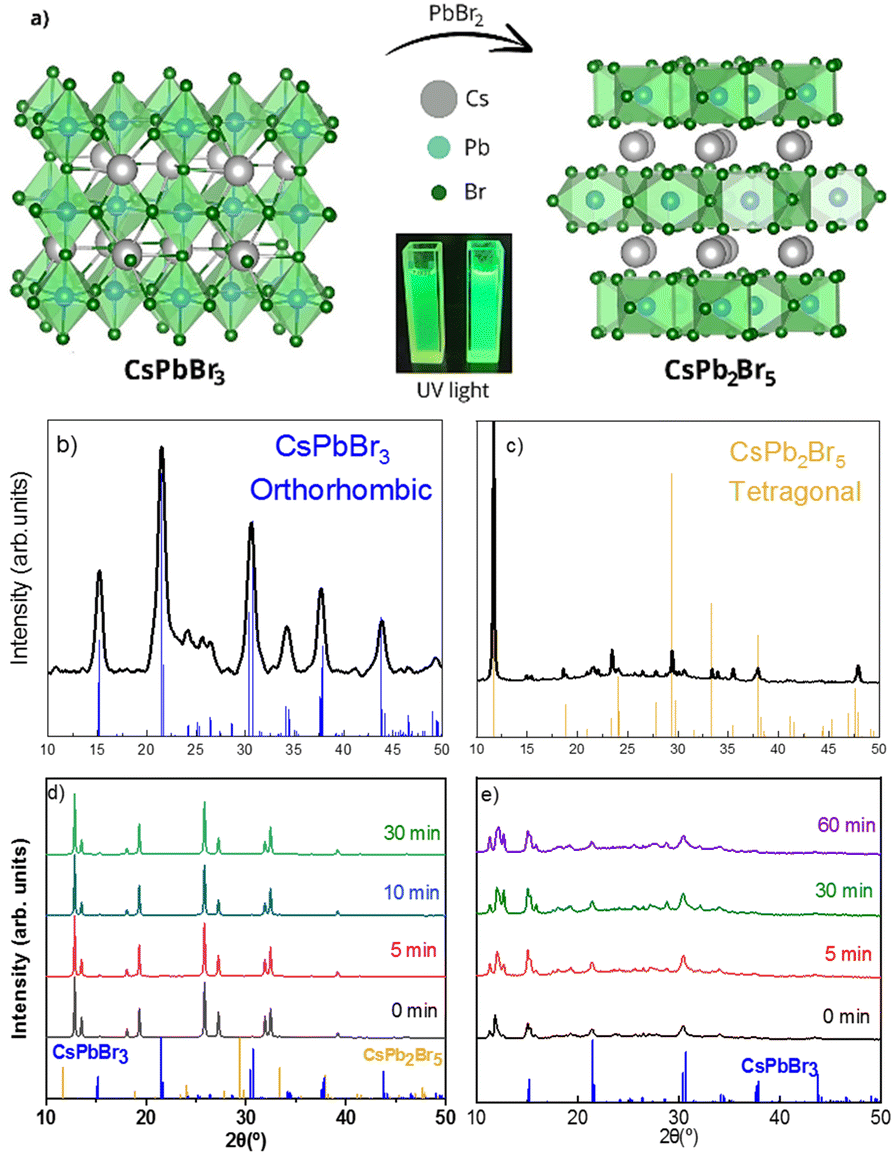 | ||
| Fig. 2 (a) Crystal structures of the CsPbBr3 orthorhombic perovskite and non-perovskite CsPb2Br5 tetragonal phase and their solutions under UV light. (b) XRD pattern of the CsPbBr3 orthorhombic phase (ICSD 243735). (c) XRD pattern of the CsPb2Br5 tetragonal phase (ICSD 254290). Note that further details on this pattern are provided in Fig. S1c (ESI†). (d) XRD patterns of CsPbBr3 with precursor dissolved in short chain ligands. (e) XRD pattern of CsPbBr3 with precursor dissolved in long chain ligands. See the main text for more details. | ||
It is interesting to note that others have obtained CsPb2Br5 NCs directly by increasing the concentration or reaction time in a standard hot-injection colloidal CsPbBr3 synthesis approach.10 To test this in our case, we modified the synthesis by doubling the volume (at the same nominal concentration of 0.5 M) of the PbBr2 precursor dissolved either in a mixture of shorter chain ligands – propionic acid (PrAc) and butylamine (BuAm) (Fig. 2d) – or longer ligands – octanoic acid (OcAc) and octylamine (OcAm) (Fig. 2e). Fig. 2d exhibits a poor correlation with the diffraction patterns of either orthorhombic CsPbBr3 or tetragonal CsPb2Br5. In contrast, the samples synthesized using longer ligands (Fig. 2e) demonstrate strong correspondence with the orthorhombic CsPbBr3 phase, albeit accompanied by unidentified diffraction peaks in low-angle regions, indicating the presence of an additional, undetermined phase. These low-angle diffraction peaks in both cases are most likely ascribed to quasi-2D Ruddlesden–Popper (RP) phases with chemical formulas BuAm2Csn−1PbnBr3n+1 and OcAm2Csn−1PbnBr3n+1.15,16 Precise determination of the “n” value proves challenging due to the potential for nanostructure self-assembly. This phenomenon is consistent with previous reports demonstrating that ligand substitution induces spontaneous self-assembly into larger, cuboidal CsPbBr3 structures composed of multiple-stacked nanoplatelets unconnected, as directly confirmed by small-angle X-ray diffraction.17 These quasi-2D crystals do not show significant changes after 30 minutes. It must be noted that, compared to the aforementioned report on direct CsPb2Br5 NC synthesis, here we use considerably shorter alkyl ligands instead of oleylamine and oleic acid, which may explain the preferential formation of the corresponding Ruddlesden–Popper phases.
Optical characterization (Fig. 3) confirms the XRD observations. The optical bandgap energy of CsPbBr3 nanoink solution was determined by the Tauc plot (see Fig. S1d, ESI†) extrapolating the straight-line portion with a bandgap energy of 2.35 eV, as expected for pure CsPbBr3 nanocrystals (NCs) reported in previous works18–21 and confirmed by the photoluminescence (PL) peak at 520 nm (Fig. 3a). CsPb2Br5 nanoinks show very similar optical properties (Fig. 3b), as has already been observed by others.1,22–25 While XRD shows a dominant CsPb2Br5 phase (Fig. 2b), we already discussed above that also CsPbBr3 impurities exist in the CsPb2Br5 solution, which, despite being small, may have an important effect particularly on the PL properties. Interestingly, the PLQY of this mixed-phase solution was higher than that of the original 3D solution (25.6% vs. 7.6%). We attribute this mainly to the surface passivating effect of adding excess PbBr2 as reported by others.26Fig. 3c and d shows the UV-vis and PL spectra of NCs synthesized with an excess of PbBr2 precursor in BuAm or OcAm. First of all, it is important to note that the synthesis time, ranging between 0 minutes and 30 minutes, does not affect the optical properties, which is in line with the very similar XRD signals observed previously (Fig. 2d and e). Again, these blue-shifted absorption and PL spectra are consistent with RP quasi-2D perovskites.27 In the case of BuAm (Fig. 3c), two absorption peaks are clearly present, pointing to the coexistence of different n-values for the RP phases. In the case of OcAm (Fig. 3d), we observe a significant shift between the main absorption and PL peaks. While the observed spectral shift could be attributed to an intrinsic Stokes shift within the RP phases, a more plausible explanation involves the presence of CsPbBr3 nanocrystals (NCs) in the solution. In fact, we observe a similar PL signal also in the BuAm-based solution when it is irradiated for longer times (see Fig. S2, ESI†), pointing towards a possible laser-induced transformation of the RP to 3D CsPbBr3.
 | ||
| Fig. 3 UV-vis absorption and PL emission spectra of (a) CsPbBr3 nanoink solution, (b) CsPb2Br5 nanoink solution, (c) CsPbBr3 with short chain ligands and (d) CsPbBr3 with long chain ligands. | ||
In summary, the as-obtained hybrid organic–inorganic quasi-2D RP phases do not seem highly stable. Therefore, for the following (thin film spray-coating and optoelectronic devices), we focus solely on the inorganic CsPbBr3 and CsPb2Br5 NC inks.
Spray-coated thin films
Thin films from the CsPbBr3 and CsPb2Br5 nanoink solutions were deposited on glass substrates by spray-coating using a simple commercial airbrush as shown in Fig. 4. Briefly, the nanoinks are placed in the airbrush cup and a nitrogen gas flow with a pressure of 0.4 bar is manually controlled to blow the inks through a 0.2 mm nozzle opening onto the substrate (around 10 cm away from the nozzle), which may be heated on a hot plate to allow instant solvent evaporation. The technique is essentially additive and arbitrary volumes may be used to increase the film thickness. Here we typically used 100 μL for one layer, with the possibility of depositing multiple layers as will be discussed hereafter. | ||
| Fig. 4 Schematic illustration of the spray-coating process and layers under UV light and in daylight. | ||
The XRD, UV-vis absorption and photoluminescence spectra of thin films obtained with CsPbBr3 and CsPb2Br5 nanoink solutions at different temperatures and with increasing number of layers are presented in Fig. 5 and 6.
 | ||
| Fig. 5 X-ray diffractograms of CsPbBr3 and CsPb2Br5 deposited at room temperature, 80 °C and 150 °C: (a) CsPbBr3 nanoink and (b) CsPb2Br5 nanoink. Reference patterns for CsPbBr3 (ICSD 243735), CsPb2Br5 (ICSD 254290) and PbBr2 (ICSD 239760) are shown in blue, orange, and green, respectively. | ||
 | ||
| Fig. 6 UV-vis absorption and normalized PL emission spectra of CsPbBr3 and CsPb2Br5 nanoinks deposited at (a) and (b) room temperature, (c) and (d) 80 °C, and (e) and (f) 150 °C; (g) PLQY correlated with temperature deposition for CsPbBr3 and CsPb2Br5. | ||
Fig. 5a shows that the films deposited from the CsPbBr3 nanoink solution present a good match with the orthorhombic crystal lattice of CsPbBr3 for the samples deposited at room temperature and 80 °C. The original nanocrystalline phase is thus maintained in the thin films. When the perovskite is deposited on a substrate at 150 °C, a signal for the tetragonal crystal lattice of the CsPb2Br5 perovskite appears along with the CsPbBr3 orthorhombic phase, thus yielding a dual-phase CsPb2Br5/CsPbBr3 film. The films prepared with CsPb2Br5 nanoink solution deposited at room temperature show a good match with the tetragonal crystal lattice of CsPb2Br5 along with minor traces of PbBr2. When increasing the deposition temperature to 80 °C and 150 °C, the peaks of PbBr2 and CsPb2Br5 increase in intensity (Fig. 5b), as expected from simple crystal sintering and growth, but no significant phase transformation is observed. Note that traces of nanocrystalline CsPbBr3 may also be present but not detected by XRD.
Fig. 6 shows the UV-vis absorption and normalized PL spectra of CsPbBr3 and CsPb2Br5 films prepared at room temperature (Fig. 6a and b), 80 °C (Fig. 6c and d), and 150 °C (Fig. 6e and f), respectively, with 1, 2, 5, and 10 layers (i.e., 100, 200, 500 and 1000 μL of nanoink solution). In all cases, a bandgap of approximately 525 nm is obtained. In detail, the samples exhibited PL maximum within the range of 515–522 nm, corresponding to energies of 2.40–2.37 eV (Table S1, ESI†). A slight red-shift of approximately 23 meV was observed in some samples with increasing film thickness. This red-shift is consistent with previously published findings, which report red shifts in the range 0–30 meV attributed to enhanced self-absorption.28,29 The increase in absorption with the number of layers translates to an obvious increase in film thickness. In Fig. S3 (ESI†), we plotted the absorbance value at 450 nm for the different compositions, temperatures, and numbers of layers. The roughly linear increase with the number of layers could serve as an indicator of layer thickness. Nonetheless, we note that absorbance values are derived from transmission measurements neglecting scattering (reflectance), which may be significant for some samples. Photoluminescence quantum yield (PLQY) (Fig. 6g) was measured for CsPbBr3 and CsPb2Br5 films prepared with 5 layers (500 μL of nanoink solution) deposited at room temperature, 80 °C and 150 °C. As hypothesized previously, the lower absorption but higher PLQY of the CsPb2Br5 films suggests that these films embed small but brightly emissive CsPbBr3 clusters, passivated by a PbBr2-rich shell.
The thickness of CsPbBr3 and CsPb2Br5 thin films deposited at 80 °C and 150 °C was characterized by atomic force microscopy (see the ESI,† Fig. S4 and S5) (samples prepared at room temperature were excluded as poor homogeneity was found already by eye). While accurate thickness determination may be difficult due to the high roughness of the films, an obvious increase from approximately 10 nm to a few hundred nanometers is observed when increasing the number of layers from 1 to 10 (see Table S2, ESI†). The morphology of CsPbBr3 and CsPb2Br5 layers was further analysed using scanning electron microscopy (SEM; Fig. 7 and Fig. S6, ESI†). Films deposited from CsPbBr3 inks show better homogeneity, with fewer aggregates compared to films deposited from CsPb2Br5 (Fig. 7). For the thicker films (10 layers), it is possible to see some cracks (Fig. S6, ESI†), but, as the films are grown by successive layer deposition, it is not obvious to determine whether the cracks penetrate the whole film thickness.
 | ||
| Fig. 7 Scanning electron microscopy (SEM) surface images of 5 layers of CsPbBr3 and CsPb2Br5 deposited (a) and (b) at 80 °C and (c) and (d) at 150 °C. | ||
The films were also characterized by X-ray photoelectron spectroscopy (XPS) to verify the oxidation states of Cs, Pb and Br (Fig. S7, ESI†) and the stoichiometry. The +1 oxidation state of Cs was verified in all cases by the peaks at 724.0 and 738.0 eV corresponding to the Cs 3d5/2 and Cs 3d3/2 orbitals. Similarly, the Br 3d5/2 and Br 3d3/2 peaks at 68.0 and 69.5 eV correspond to the expected bromide signals for CsPbBr3 and CsPb2Br5. Eventually, the main Pb 4f signals at 138.0 and 143.0 eV are consistent with Pb(II), with a minor contribution at lower binding energies ascribed to Pb(0). This metallic lead has been extensively observed previously in lead halide perovskites and may be induced by ionizing radiation, such as that employed in XPS.30 The stoichiometry derived from XPS for films deposited at 80 °C and 150 °C from both inks is summarized in Table 1.
| Nanoink | Deposition temperature (°C) | Cs at% | Pb at% | Br at% |
|---|---|---|---|---|
| CsPbBr3 | 80 | 18.34 (20) | 22.00 (20) | 59.67 (60) |
| CsPbBr3 | 150 | 17.81 (20) | 22.67 (20) | 59.52 (60) |
| CsPb2Br5 | 80 | 15.96 (12.5) | 24.39 (25) | 59.65 (62.5) |
| CsPb2Br5 | 150 | 15.05 (12.5) | 23.17 (25) | 61.78 (62.5) |
Overall, the obtained stoichiometries are close to the expected values (given in parentheses in Table 1) for CsPbBr3 and CsPb2Br5. However, we observe a slight Pb-rich (Cs-poor) composition for films prepared from CsPbBr3, which may be related to a preferential PbBr2 film termination, considering that XPS is a surface-sensitive technique. The opposite is observed for films deposited from CsPb2Br5, where a Cs-rich composition is observed. Nonetheless, as already noted in Fig. 5, it is known that the films are not phase-pure, so the slight differences between expected and obtained stoichiometries may be simply due to the coexistence of different phases.31,32
Lateral photodetectors
We incorporated the spray-coated thin films into lateral photodetectors. For this purpose, we deposited nanoink solutions onto interdigitated indium tin oxide (ITO) substrates, each having four identical pixels with a 40 μm spacing between the electrodes (see Fig. S8, ESI,† for a schematic representation and device details), and measured current–voltage (I–V) characteristics under different illumination conditions. As a preliminary study, we separately evaluated the effect of layer thickness at a fixed deposition temperature (Fig. S9a, ESI†), and the effect of the deposition temperature at a fixed film thickness (Fig. S9b, ESI†), both in the dark and with white light illumination (1 sun). Based on these results, we chose 5 layers and a deposition temperature of 150 °C as optimal conditions to maximize photocurrent, maintaining a similarly low dark current for all films. Then, I–V curves were measured under 405 nm illumination at different intensities. Fig. 8a and b presents the representative I–V curves (Fig. S10, ESI,† shows good homogeneity among different pixels). Note that the dark I–V characteristics are very similar for the two compounds due to the very high dark resistivity of these types of materials. However, the photocurrent of devices based on CsPbBr3 was found to increase up to almost three orders of magnitude compared to the dark current, when increasing the light intensity up to 200 mW cm−2. On the other hand, the CsPb2Br5 samples showed a much reduced response, with a maximum variation of the photocurrent within one order of magnitude. The lower photoconductivity might originate from the reduced connectivity of the lead halide within the layered CsPb2Br5 crystal structure. It could be expected that the preferential orientation of CsPb2Br5 on the substrate could favor lateral transport, but as the typical crystal size is small relative to the electrode spacing, this is probably not significant (as opposed to having a single nanosheet bridging two electrodes, which is not the case here). Both materials show a linear increase of the photocurrent as a function of the input light power (Fig. 8c). A higher slope of the current–intensity curve (sensitivity) is observed for the CsPbBr3 devices, although some saturation of the photocurrent might be observed at high illumination intensity. Additionally, the photocurrent was measured within the voltage range of −50 V to 50 V with a reverse sweep to assess the hysteresis caused by charge accumulation at the non-ohmic ITO/semiconductor interfaces and by ionic migration (see Fig. S11a and b, ESI†). Under both dark and light conditions, both CsPbBr3 and CsPb2Br5 samples demonstrated consistent I–V curves, with negligible hysteresis (the curves are in the logarithmic scale). This indicates a rather low concentration of ionic species in the material. The dynamic response of both photodetectors was also evaluated as a function of light intensity (see Fig. S11c and d, ESI†). It must be noted that low response times as well as other relatively poor photodetector metrics, such as responsivity and linear dynamic range, which can partly be derived from Fig. 8, may be intrinsic to the lateral photoconductor geometry and therefore not directly comparable to vertical photodiodes. On/off ratios, responsivity and EQE spectra have been evaluated, showing superior performance from the CsPbBr3 devices (Fig. S12, ESI†), also in terms of switching speed (Fig. S13, ESI†). Regarding stability, it is interesting to note that, after 9 months of storage in a nitrogen-filled glovebox, the devices remain essentially unchanged (see Fig. S14, ESI†).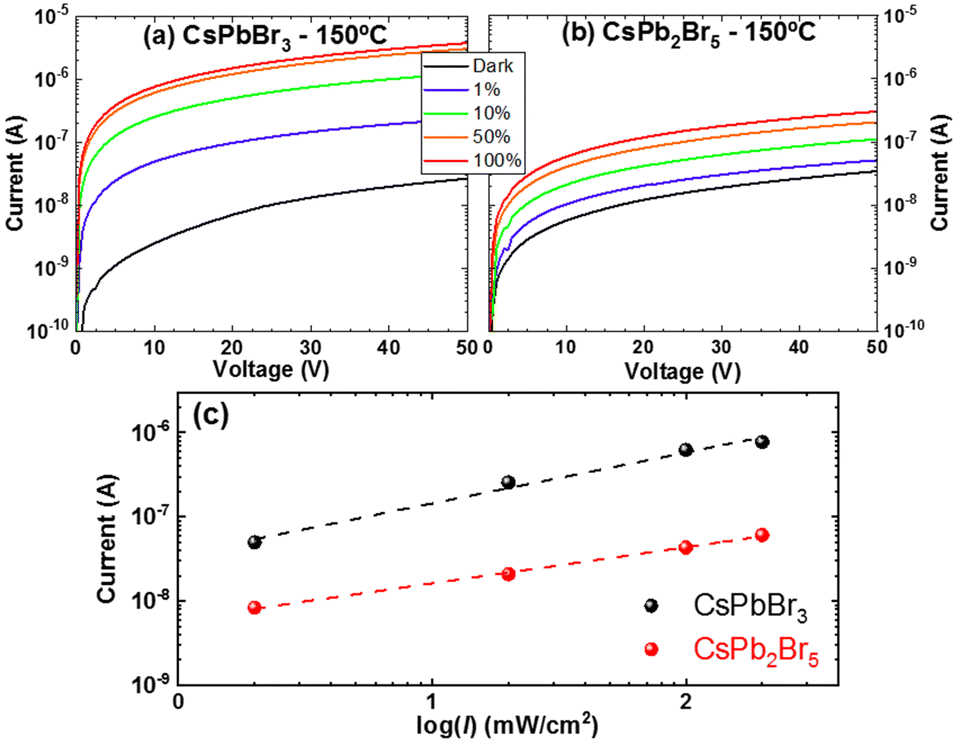 | ||
| Fig. 8 Current–voltage curves of (a) CsPbBr3 and (b) CsPb2Br5 at 150 °C under various illumination powers using a blue light LED as a light source (100% power intensity equals to 200 mW cm−2). (c) Current–intensity dependence of CsPbBr3 and CsPb2Br5 at 150 °C at 10 V plotted based on previous measurements and fitted with a linear function. | ||
Conclusions
In conclusion, we have demonstrated a simple approach for the deposition of inorganic CsPbBr3, CsPb2Br5 and dual-phase CsPbBr3–CsPb2Br5 thin films combining low-temperature colloidal synthesis and post-synthesis modifications together with spray-coating using commercially available airbrush technology. As a result, high-quality perovskite and perovskite-related thin films are obtained with significant light absorption and emission in the visible range. Lateral photodetectors have been fabricated and dual-phase films have shown the best performance, with an increase of up to 3 orders of magnitude in photocurrent with respect to dark current under monochromatic blue light. These findings hold significant promise for the advancement of profitable perovskite optoelectronics, providing a simple and scalable route towards device fabrication. Future studies will focus on controlling the film morphology (possibly by optimizing the viscosity and wetting properties of the solvent and surface) in order to improve charge transport and to apply these materials in more complex functional devices such as solar cells and LEDs.Author contributions
The manuscript was written through contributions of all authors.Data availability
In accordance with the FAIR principles, the data for this article are available at: https://repositorio.upct.es/entities/person/7ba1ef8c-072d-4f1e-9eaf-4ce322a54e4f?tab=isAuthorOfPublication.Conflicts of interest
There are no conflicts to declare.Acknowledgements
The authors acknowledge funding for project TED2021-129609BI00 funded by MCIN/AEI/10.13039/501100011033 and the European Union NextGenerationEU/PRTR; grant CNS2023-144331 funded by MCIU/AEI/10.13039/501100011033 and the European Union Next Generation EU/PRTR; and grant PID2022-139191OB-C32 funded by MCIN/AEI. F. P. acknowledges funding for grant RYC2020-028803-I funded by MCIN/AEI/10.13039/501100011033 and “ESF Investing in your future”. The authors also acknowledge funding from the Generalitat Valenciana, project CISEJI/2022/43 and CIPROM/2022/57. K. J. acknowledges funding from Fundación Séneca fellowship 22747/FPI/24, Fundación Séneca, Región de Murcia (Spain).Notes and references
- X. Zhang, B. Xu, J. Zhang, Y. Gao, Y. Zheng, K. Wang and X. W. Sun, Adv. Funct. Mater., 2016, 26, 4595–4600 CrossRef CAS.
- B.-S. Zhu, H.-Z. Li, J. Ge, H.-D. Li, Y.-C. Yin, K.-H. Wang, C. Chen, J.-S. Yao, Q. Zhang and H.-B. Yao, Nanoscale, 2018, 10, 19262–19271 RSC.
- C. Zhang, Z. Wang, M. Wang, J. Shi, J. Wang, Z. Da, Y. Zhou, Y. Xu, N. V. Gaponenko and A. S. Bhatti, ACS Appl. Mater. Interfaces, 2023, 15, 35216–35226 CrossRef CAS PubMed.
- Z. Sun, Y. Wang, Y. Liu, R. Liu, T. Chen, S. Ye, N. Lai, H. Cui, F. Lin, R. Wang, J. Yang, S. Ke and C. Wang, ACS Appl. Nano Mater., 2024, 7, 11785–11793 CrossRef CAS.
- R. Wang, Z. Li, S. Li, P. Wang, J. Xiu, G. Wei, H. Liu, N. Jiang, Y. Liu and M. Zhong, ACS Appl. Mater. Interfaces, 2020, 12, 41919–41931 CrossRef CAS PubMed.
- X. Zhang, Z. Jin, J. Zhang, D. Bai, H. Bian, K. Wang, J. Sun, Q. Wang and S. F. Liu, ACS Appl. Mater. Interfaces, 2018, 10, 7145–7154 CrossRef CAS PubMed.
- G. Tong, H. Li, D. Li, Z. Zhu, E. Xu, G. Li, L. Yu, J. Xu and Y. Jiang, Small, 2018, 14, 1702523 CrossRef PubMed.
- M. Yang, J. Yu, S. Jiang, C. Zhang, Q. Sun, M. Wang, H. Zhou, C. Li, B. Man and F. Lei, Opt. Exp., 2018, 26, 20649–20660 CrossRef CAS PubMed.
- Q. A. Akkerman, M. Gandini, F. Di Stasio, P. Rastogi, F. Palazon, G. Bertoni, J. M. Ball, M. Prato, A. Petrozza and L. Manna, Nat. Energy, 2016, 2, 1–7 Search PubMed.
- P. Acharyya, P. Pal, P. K. Samanta, A. Sarkar, S. K. Pati and K. Biswas, Nanoscale, 2019, 11, 4001–4007 RSC.
- J. Deng, J. Xun, W. Shen, M. Li and R. He, ACS Appl. Nano Mater., 2021, 4, 9213–9222 CrossRef CAS.
- Z. Zhang, Y. Zhu, W. Wang, W. Zheng, R. Lin and F. Huang, J. Mater. Chem. C, 2018, 6, 446–451 RSC.
- Z.-P. Huang, B. Ma, H. Wang, N. Li, R.-T. Liu, Z.-Q. Zhang, X.-D. Zhang, J.-H. Zhao, P.-Z. Zheng, Q. Wang and H.-L. Zhang, J. Phys. Chem. Lett., 2020, 11, 6007–6015 CrossRef CAS PubMed.
- One-Pot Synthesis of Stable CsPbBr3@CsPb2Br5 Core–Shell Heteronanocrystals with Controlled Permeability to Halide Ions | Chem. Mater., https://pubs.acs.org/doi/10.1021/acs.chemmater.3c01280, (accessed March 13, 2025) Search PubMed.
- M. Rahil, R. M. Ansari, C. Prakash, S. S. Islam, A. Dixit and S. Ahmad, Sci. Rep., 2022, 12, 2176 CrossRef CAS PubMed.
- G. Liu, C. Qiu, B. Tian, X. Pan, D. Ding, Y. Chen, C. Ren, T. He, Y. Shi, C. Su, Y. Li, Y. Gao and D. Fan, ACS Appl. Electron. Mater., 2019, 1, 2253–2259 CrossRef CAS.
- Spontaneous Self-Assembly of Cesium Lead Halide Perovskite Nanoplatelets into Cuboid Crystals with High Intensity Blue Emission, https://advanced.onlinelibrary.wiley.com/doi/epdf/10.1002/advs.201900462, (accessed March 13, 2025).
- D. A. Idosa, M. Abebe, D. Mani, A. Thankappan, S. Thomas, F. G. Aga and J. Y. Kim, Photonics, 2023, 10, 802 CrossRef CAS.
- W. Yan, L. Mao, P. Zhao, A. Mertens, S. Dottermusch, H. Hu, Z. Jin and B. S. Richards, Opt. Express, 2020, 28, 15706–15717 CrossRef CAS PubMed.
- K. Sung Hun, K.-D. Park and H. S. Lee, Energies, 2021, 14, 275 CrossRef.
- L. Protesescu, S. Yakunin, M. I. Bodnarchuk, F. Krieg, R. Caputo, C. H. Hendon, R. X. Yang, A. Walsh and M. V. Kovalenko, Nano Lett., 2015, 15, 3692–3696 CrossRef CAS PubMed.
- Q. Han, S. Gong, H. Yu and W. Wu, Opt. Mater., 2023, 137, 113477 CrossRef CAS.
- K. Du, L. He, S. Song, J. Feng, Y. Li, M. Zhang, H. Li, C. Li and H. Zhang, Adv. Funct. Mater., 2021, 31, 2103275 CrossRef CAS.
- J. Lv, L. Fang and J. Shen, Mater. Lett., 2018, 211, 199–202 CrossRef CAS.
- P. Li, C. Hu, L. Zhou, J. Jiang, Y. Cheng, M. He, X. Liang and W. Xiang, Mater. Lett., 2017, 209, 483–485 CrossRef CAS.
- M. I. Bodnarchuk, S. C. Boehme, S. ten Brinck, C. Bernasconi, Y. Shynkarenko, F. Krieg, R. Widmer, B. Aeschlimann, D. Günther, M. V. Kovalenko and I. Infante, ACS Energy Lett., 2019, 4, 63–74 CrossRef CAS PubMed.
- S. Bhaumik, S. A. Veldhuis, Y. F. Ng, M. Li, S. K. Muduli, T. C. Sum, B. Damodaran, S. Mhaisalkar and N. Mathews, Chem. Commun., 2016, 52, 7118–7121 RSC.
- D. Baranov, S. Toso, M. Imran and L. Manna, J. Phys. Chem. Lett., 2019, 10, 655–660 CrossRef CAS PubMed.
- J. S. van der Burgt, J. J. Geuchies, B. van der Meer, H. Vanrompay, D. Zanaga, Y. Zhang, W. Albrecht, A. V. Petukhov, L. Filion, S. Bals, I. Swart and D. Vanmaekelbergh, J. Phys. Chem. C, 2018, 122, 15706–15712 CrossRef CAS PubMed.
- Z. Dang, J. Shamsi, F. Palazon, M. Imran, Q. A. Akkerman, S. Park, G. Bertoni, M. Prato, R. Brescia and L. Manna, ACS Nano, 2017, 11, 2124–2132 CrossRef CAS PubMed.
- Deconvoluting the energy transport mechanisms in all-inorganic CsPb2Br5/CsPbBr3 perovskite composite systems | APL Materials | AIP Publishing, https://pubs.aip.org/aip/apm/article/10/3/031101/2834855, (accessed March 28, 2025).
- R. Zhi, J. Hu, S. Yang, C. Perumal Veeramalai, Z. Zhang, M. I. Saleem, M. Sulaman, Y. Tang and B. Zou, J. Alloys Compd., 2020, 824, 153970 CrossRef CAS.
Footnote |
| † Electronic supplementary information (ESI) available. See DOI: https://doi.org/10.1039/d5tc00346f |
| This journal is © The Royal Society of Chemistry 2025 |