DOI:
10.1039/D5TC00211G
(Paper)
J. Mater. Chem. C, 2025,
13, 8198-8204
Fabrication of large-area nanostructures of pine needles with a dewdrop array for surface-enhanced Raman spectroscopy†
Received
17th January 2025
, Accepted 5th March 2025
First published on 6th March 2025
Abstract
Surface-enhanced Raman spectroscopy (SERS) depends on the development of a nanostructured substrate on which the excitation of a localized surface plasmon enhances the Raman scattering signals. Herein, we proposed a large-area three-dimensional (3D) pine needle with a dewdrop array (PNDA) nanostructure that can be easily fabricated via a film deposition technique with the help of a self-assembled polystyrene microsphere template and ultra-thin anodized aluminum oxide mask. Electromagnetic hotspots generated at the cracks or gaps between adjacent island structures of the PNDA are responsible for the SERS enhancement factor of 6.7 × 10⁶ when the structural parameters of the PNDA substrate are optimized. Experiments demonstrated that the rhodamine 6G (R6G) molecule can be probed with the PNDA substrate at the lowest concentration of 10−9 M using SERS. The homogeneity of the substrate was confirmed by verifying the relative standard deviation (RSD) of Raman spectra at different sites (6.5% at 611 cm−1 and 8.3% at 1652 cm−1). Moreover, crystal violet (CV) molecules were probed using our SERS experiment at the lowest detection concentration of 10−8 M. The results confirm that the PNDA structure is a reliable and sensitive SERS substrate to detect trace amounts of pollutants in an aquatic environment.
1. Introduction
Surface-enhanced Raman spectroscopy (SERS) is a sensitive vibrational spectroscopy technique that can detect a molecular fingerprint at extremely low concentration. SERS technology has been broadly applied in various fields of biomedicine,1–4 environment monitoring,5,6 food safety7–10 and photocatalysis.11–13 The high sensitivity of SERS detection is attributed to the electromagnetic “hotspots” at the sharp tip14,15 or confined gap16–18 of the metallic nanostructures because of their local surface plasmon resonance. For the development of a sensitive SERS technique, the fabrication of metallic nanostructures that allow dense and uniform “hotspots” is particularly important.
Classical top-down techniques of electron beam lithography (EBL),19,20 nanoimprint lithography (NIL)21,22 and focused ion beam (FIB) lithography23,24 have been utilized to fabricate ordered nanostructures as SERS substrates owing to their accurate controllability and remarkable uniformity. However, these techniques suffer from the limitations of being expensive, having a low throughput and being time-consuming. To circumvent the above limitations, certain low-cost fabrication methods, including displacement Talbot lithography (DTL),25 electrodeposition,26,27 microsphere lithography28–30 and anodized aluminum oxide (AAO),31–33 were developed to fabricate large-area ordered SERS substrates. Among these low-cost methods, fabrication with a monolayer of polystyrene (PS) microsphere template34,35 or ultra-thin AAO (UTAAO) mask36,37 is more attractive owing to its high throughput and low cost. Many two-dimensional (2D)18,34,36 and three-dimensional (3D)11,13,38,39 ordered arrays of nanostructures have been fabricated using the self-assembled PS microsphere template or UTAAO mask. Compared with 2D nanostructures, 3D plasmonic nanostructures can yield additional electromagnetic “hotspots,” which are helpful for enhancing SERS sensitivity.13,29,40 Therefore, the development of large-area 3D-ordered SERS substrates using cheap and facile approaches are worth exploring.
Herein, we proposed a large-area 3D pine needle with a dewdrop array (PNDA) substrate fabricated via the simple deposition of silica and silver film with a self-assembled PS microsphere template and UTAAO mask. Because of the prominent enhancement of the electric field at the cracks and gaps between adjacent island structures, SERS with a PNDA substrate was used to probe rhodamine 6G (R6G) molecules with high sensitivity and good uniformity at different measurement sites. Using the PNDA substrate, crystal violet (CV) molecules, known as a hazardous pollutant in water, were sensitively detected using SERS with a linear correlation between the Raman signal and concentration. Results indicate that the PNDA structure is a reliable and sensitive SERS substrate to probe the trace amount of pollutants in an aquatic environment.
2. Experimental
2.1. Materials
Rhodamine 6G (R6G), crystal violet (CV), silver wire (99.9%), acetone (AR, GC ≥ 99.5%), ethanol (AR, GC ≥ 99.7%), sulfuric acid (H2SO4, AR, GC ≥ 95%) and hydrogen peroxide (H2O2, AR, GC ≥ 30%) were purchased from Sinopharm Chemical Reagent Co., Ltd. PS microspheres (diameters of 500, 1000 and 2000 nm) were obtained from Huge Biotechnology (Shanghai). The UTAAO mask (125 nm period, 100 nm pore diameter, 400 nm thickness) was obtained from TopMembranes Technology (Shenzhen). The 18.0 MΩ deionized water utilized for the experiments was supplied by our laboratory.
2.2. Fabrication of PNDA
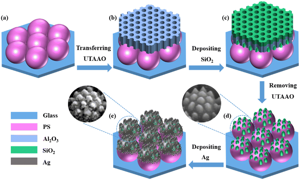
Glass slides were sequentially subjected to ultrasonic cleaning in acetone, ethanol, piranha solution (98% H2SO4![[thin space (1/6-em)]](https://www.rsc.org/images/entities/char_2009.gif) :30% H2O2 = 3:1) and deionized water. As can be seen in Fig. 1, the PNDA substrate was fabricated by depositing silica and silver through the UTAAO mask and self-assembled PS microsphere template. First, a centimeter-sized monolayer of PS microsphere array was self-assembled at the gas–liquid interface34,35 and then transferred to a cleaned glass slide (Fig. 1(a)). After drying naturally, the PS microsphere array on the glass slide was placed on a hot plate and baked at 108 °C for 10 min. Second, a UTAAO mask was transferred to the surface of the PS microspheres array (Fig. 1(b)). The commercially bought UTAAO was prudently shifted onto the hydrophilic and smooth Si substrate, and then, the UTAAO held by a Si substrate was gently inserted in the deionized water. The UTAAO mask floated on the water surface because of surface tension, and then, the UTAAO was laid on the PS microsphere array by inserting the substrate prepared in the first step. Third, silicon oxide (SiO2) was deposited on the surface of PS microspheres through the holes of the UTAAO mask (Fig. 1(c)) using electron beam (E-beam) evaporation at the rate of 1 Å s−1. SiO2 nanopillars were maintained on the surface of PS microspheres after blowing off the UTAAO mask with nitrogen gas (Fig. 1(d)). Finally, Ag was deposited through high-vacuum thermal evaporation at a rate of 1 Å s−1 (Fig. 1(e)), and then, a centimeter-sized PNDA substrate was obtained.
:30% H2O2 = 3:1) and deionized water. As can be seen in Fig. 1, the PNDA substrate was fabricated by depositing silica and silver through the UTAAO mask and self-assembled PS microsphere template. First, a centimeter-sized monolayer of PS microsphere array was self-assembled at the gas–liquid interface34,35 and then transferred to a cleaned glass slide (Fig. 1(a)). After drying naturally, the PS microsphere array on the glass slide was placed on a hot plate and baked at 108 °C for 10 min. Second, a UTAAO mask was transferred to the surface of the PS microspheres array (Fig. 1(b)). The commercially bought UTAAO was prudently shifted onto the hydrophilic and smooth Si substrate, and then, the UTAAO held by a Si substrate was gently inserted in the deionized water. The UTAAO mask floated on the water surface because of surface tension, and then, the UTAAO was laid on the PS microsphere array by inserting the substrate prepared in the first step. Third, silicon oxide (SiO2) was deposited on the surface of PS microspheres through the holes of the UTAAO mask (Fig. 1(c)) using electron beam (E-beam) evaporation at the rate of 1 Å s−1. SiO2 nanopillars were maintained on the surface of PS microspheres after blowing off the UTAAO mask with nitrogen gas (Fig. 1(d)). Finally, Ag was deposited through high-vacuum thermal evaporation at a rate of 1 Å s−1 (Fig. 1(e)), and then, a centimeter-sized PNDA substrate was obtained.
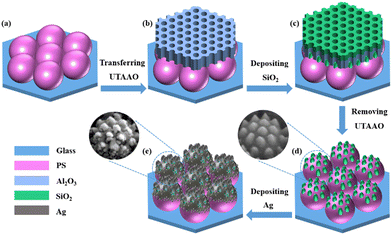 |
| | Fig. 1 Schematic of the fabrication procedure. (a) PS microsphere array on a cleaned glass slide. (b) UTAAO mask on the surface of PS microspheres array of (a). (c) SiO2 deposition on the surface of (b). (d) SiO2 nanopillars on the surface of PS microspheres array of (a). (e) Ag deposition on the surface of (d). | |
Surface morphology of all samples was characterized using scanning electron microscopy (SEM) (Hitachi, SU8220) at 3 kV. Moreover, the typical SEM images of the samples in different fabrication stage are shown in Fig. S1 (ESI†), and the low-magnification SEM images of the large area of SiO2 nanopillars on the PS array and the PNDA structure are shown in Fig. S2 (ESI†).
2.3. Raman spectrum measurement
R6G molecules were used as probing analytes to estimate the Raman performance of the PNDA substrate. The sample was excited using a 532 nm laser with an objective lens (40×, NA = 0.6), the Raman scattering light was collected after a long pass filter and the Raman spectrum was recorded using the HORIBA iHR550 spectrometer. The excitation laser power of 0.05 mW was used for the R6G probe and 0.1 mW for the CV molecules. The accumulation time was set as 1 s to obtain the Raman spectra of R6G and 5 s to obtain the Raman spectra of CV. After eliminating the baseline and fluorescence background using Origin, clean Raman spectra were obtained.
2.4. Electromagnetic field simulation
Distribution of the electromagnetic field in the nanostructure was numerically simulated using the 3D finite-difference time-domain (FDTD) method. The morphology and geometric parameters of nanostructures was obtained from the corresponding SEM images in the simulation. During the FDTD simulation, periodic boundary conditions are imposed along the x- and y-axes, while a perfectly matched layer (PML) is employed at the boundary of the z-axis. A 532 nm plane wave, linearly polarized along the x-direction, is incident on the sample along the z-axis. The y-normal monitor was used to retrieve the near-field electric field distribution within the x–z plane for the nanostructure. A grid size of 1 nm was set to ensure simulation accuracy.
3. Results and discussion
3.1. Parameter optimization for PNDA
As shown in Fig. 1, the PNDA substrate was fabricated when proper fabrication parameters were chosen. To promote the SERS performance, many fabrication parameters, including the deposition thickness of Ag and SiO2 and the size of PS microspheres, were optimized. We fabricated substrates with different parameters and then characterized the surface morphology through SEM and the SERS of R6G probes on substrates. The detailed influences of every parameter are presented in the following sections.
3.1.1. Influence of Ag deposition thickness.
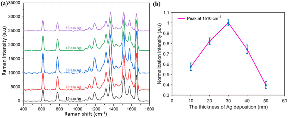
The deposition thickness of Ag is the most important parameter that determines the surface morphology of the substrate. To obtain the optimal Ag thickness, we fabricated the substrate according to the fabrication procedure shown in Fig. 1. Moreover, PS microspheres with a diameter of 500 nm were used, and the deposition thickness of SiO2 was 200 nm. Five different substrates were fabricated with different Ag thicknesses of 10, 20, 30, 40 and 50 nm. Here, the deposition thickness indicates the duration of deposition at the specified rate, rather than the actual material thickness, due to the rough and discontinuous nature of the film. The SEM images presented in Fig. S3 (ESI†) show the evolution of the surface morphology as the deposition thickness of Ag (ranging from 10 to 50 nm) increases. The seed particles are randomly created initially, and these particles then grow and finally connect to each other to form a continuous Ag film. Five different substrates were soaked in 10−5 M R6G solution for 2 h and then dried using nitrogen gas. Raman spectra of R6G probes on the different substrates are shown in Fig. 2(a). The relative intensity of the characteristic Raman peak at 1510 cm−1 can be seen in Fig. 2(b). The strongest Raman enhancement is achieved for the Ag deposition thickness of 30 nm. According to this experiment result, all PNDA substrates were fabricated with the Ag deposition thickness of 30 nm for subsequent analyses.
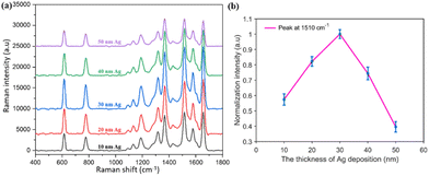 |
| | Fig. 2 (a) Raman spectra corresponding to 10−5 M R6G absorbed onto five different substrates with various thicknesses of Ag deposition. (b) Normalized Raman intensities corresponding to the typical peak at 1510 cm−1 for 10−5 M R6G under a variety of Ag deposition thicknesses. | |
3.1.2. Influence of SiO2 deposition thickness.
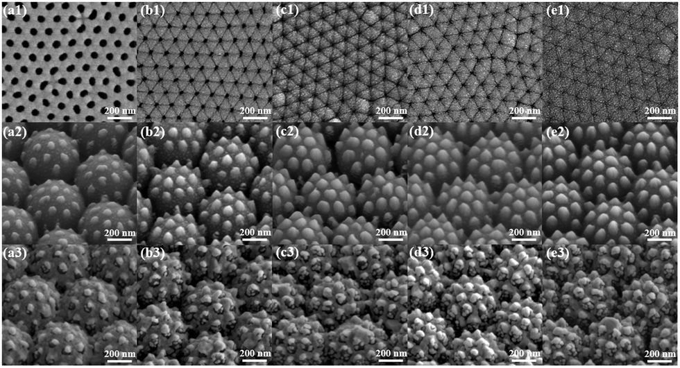
SiO2 nanopillars are fabricated on the surface of the PS microsphere by the deposition of SiO2 through the nanometric pores of AAO using E-beam evaporation. The size of the SiO₂ nanopillar can be readily controlled by adjusting the final evaporation thickness. We fabricated five substrates with different SiO2 evaporation thicknesses of 50, 100, 150, 200 and 250 nm. The diameter of 500 nm was chosen for PS microspheres, and the Ag deposition thickness was 30 nm for all five samples. The surface morphologies of AAO, PS microsphere array with SiO2 nanopillars and the final PNDA substrate were inspected using SEM for all samples.
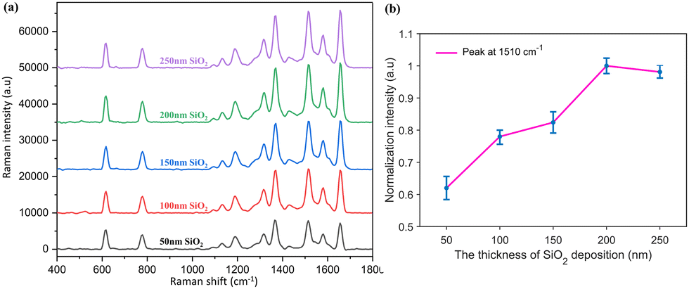
As shown in Fig. 3(a1–e1), the nanopores of AAO gradually shrink because of the deposition of SiO2 and are almost blocked at the SiO2 deposition thickness of 250 nm. The size of the SiO2 nanopillars (Fig. 3(a2–e2)) also increases as the SiO2 deposition thickness increases before the nanopores of AAO are blocked. The SEM images of the different PNDA substrates after Ag deposition are displayed in Fig. 3(a3–e3). The Ag film breaks into additional nanograins as the size of SiO2 nanopillars grows, and therefore, many gaps and cracks are introduced in the Ag film. PNDA substrates with different sizes of SiO2 nanopillars were soaked in 10−5 M R6G for 2 h and then dried using nitrogen gas. Raman spectra of R6G probes for the different substrates were obtained (Fig. 4(a)), and the relative intensities for the typical Raman peak at 1510 cm−1 of R6G molecules are illustrated in Fig. 4(b). As revealed by the Raman spectra, a more pronounced enhancement of the Raman signal is observed for substrates fabricated with larger SiO₂ nanopillars. Note that Raman intensity is slightly weakened for the 250-nm-sized SiO2 deposition thickness possibly because the SiO2 nanopillar size fluctuates when the nanopores of AAO are almost blocked. Therefore, we adopted the SiO2 deposition thickness of 200 nm as the optimal choice for subsequent analyses.
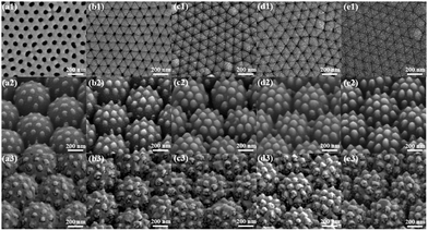 |
| | Fig. 3 SEM images of the surface morphologies of various PNDA structures with SiO2 deposition thickness of (a1)–(a3) 50, (b1)–(b3) 100, (c1)–(c3) 150, (d1)–(d3) 200, and (e1)–(e3) 250 nm. (a1)–(e1) Surface morphologies of the pore diameter of different samples. (a2)–(e2) Surface morphologies of SiO2 nanopillars growing on surface of the PS microsphere. (a3)–(e3) Surface morphologies of different PNDA structures. The white line represents 200 nm. | |
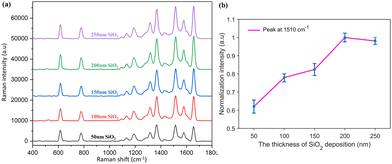 |
| | Fig. 4 (a) Raman spectra corresponding to 10−5 M R6G absorbed on a variety of PNDA structures featuring differing SiO2 deposition thicknesses. (b) Normalization of Raman intensities for a typical peak at 1510 cm−1 for 10−5 M R6G solution under the diverse SiO2 deposition thicknesses. | |
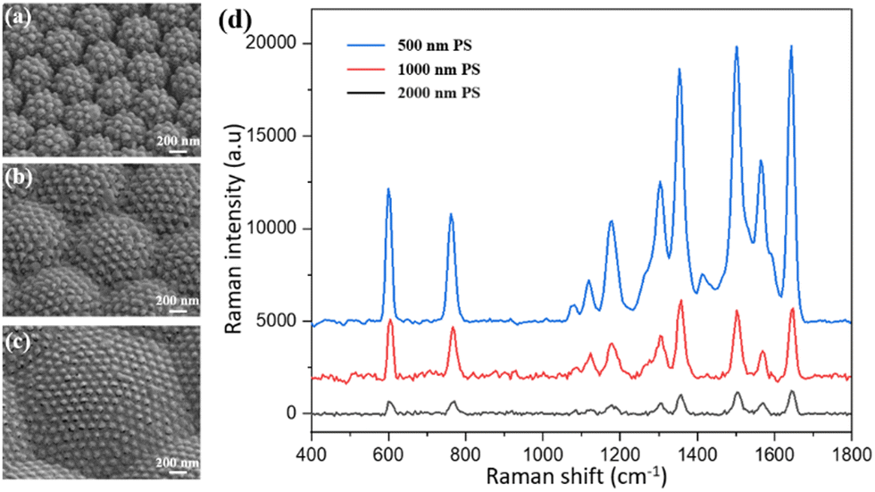
3.1.3. Influence of the size of PS microspheres.
The size of PS microspheres has considerable influence on the surface morphology of the PNDA substrate. To determine the optimal size of PS microspheres, we fabricated different PNDA substrates on PS microspheres with different diameters of 500, 1000 and 2000 nm. The optimal deposition thickness of 30 nm for Ag and 200 nm for SiO2 were used for fabrication. SEM images of various PNDA substrates fabricated on different PS microspheres are displayed in Fig. 5(a–c). The number of independent metal particles on the surface of the PS microspheres reduces with increase in the diameter of PS microspheres, and the PS microspheres stick together when the diameter is 1000 and 2000 nm. However, the microspheres are independent of each other at a diameter of 500 nm, as seen in Fig. 5(a–c). Different PNDA substrates with different diameters of PS microspheres were soaked in 10−5 M R6G for 2 h and dried using nitrogen gas, and then, the Raman spectra of R6G molecules on different samples were obtained and are presented in Fig. 5(d). As can be seen in Fig. 5(d), the Raman intensities of characteristic peaks at different positions gradually decreases with the increase in the diameter of PS microspheres. The best Raman intensity was observed for PS microspheres at a diameter of 500 nm. Therefore, the PNDA structure fabricated using 500-nm-diameter PS microspheres was selected for further study.
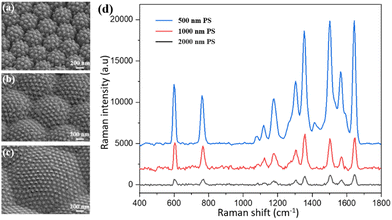 |
| | Fig. 5 SEM images showcasing different PNDA substrates with different sizes of PS microspheres: (a) with a diameter of 500, (b) 1000, and (c) 2000 nm, where the white line represents 200 nm. (d) Raman spectra of 10−5 M R6G absorbed on different PNDA substrates featuring different sizes of PS microspheres. | |
3.2. SERS performance of the PNDA substrate
The PNDA substrate was fabricated with the following optimal parameters: an Ag deposition thickness of 30 nm, SiO2 deposition thickness of 200 nm and PS microsphere diameter of 500 nm. The enhancement of Raman scattering in the optimized PNDA substrate was clarified by comparing the Raman spectra of R6G molecules on the PNDA substrate and the substrates that comprise PS microspheres covered in Ag or SiO2 nanopillars covered in Ag. Moreover, the SERS performance of the PNDA substrate, including sensitivity, uniformity and versatility, was investigated.
3.2.1. Comparative investigation of SERS substrates.
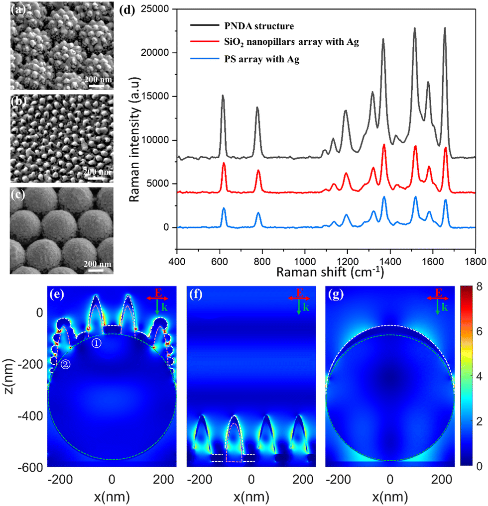
The advantages of the PNDA substrate was demonstrated through comparative measurements of the Raman spectra of R6G molecules on various substrates. For comparison, we fabricated three different substrates: the optimized PNDA substrate, the SiO2 nanopillars array covered with 30 nm Ag, and 500-nm-sized PS microsphere array covered with 30 nm Ag. The surface morphologies of all three samples were characterized using SEM images (Fig. 6(a–c)). The combination of PS microspheres and SiO2 nanopillars leads to a sharp slope, especially for the SiO2 nanopillar located at the edge of the PS microsphere (the schematic in Fig. S4, ESI†). Under these conditions, the growth of Ag on the steep slopes can be considered as oblique angle vapor deposition,41 which leads to the formation of island-like metal particles. This is in contrast to the vertical deposition42 that occurs on the tops of the SiO₂ nanopillars. Consequently, a silver block forms on top of each SiO₂ nanopillar, accompanied by some smaller particles around the nanopillars. We refer to this structure graphically as PNDA.
 |
| | Fig. 6 SEM images of three SERS substrates: (a) the optimized PNDA, (b) the SiO2 nanopillars array covered with 30 nm Ag, and (c) the 500 nm PS microsphere array covered with 30 nm Ag. (d) Raman spectra of 10−5 M R6G absorbed onto three different substrates: the optimized PNDA (black line), the SiO2 nanopillars array covered with 30 nm Ag (red line), and the 500 nm PS microsphere array covered with 30 nm Ag (blue line). The simulated electric field distributions across a perpendicular cross-section: (e) the optimized PNDA, (f) the SiO2 nanopillars array covered with 30 nm Ag, and (g) the 500 nm PS microsphere array covered with 30 nm Ag. | |
All the samples were soaked in 10−5 M R6G solutions for 2 h, and then, the Raman spectrum was obtained. As can be seen in Fig. 6(d), the Raman spectrum is distinctly enhanced more by the PNDA substrate than by the other two substrates. Quantitatively, the SERS of the PNDA substrate at 1510 cm−1 is approximately threefold stronger than that of the SiO2 nanopillars array substrate covered with 30 nm Ag and fourfold stronger than that of 500 nm PS microsphere array substrate covered with 30 nm Ag. The different Raman intensities can be attributed to the different electromagnetic enhancement of substrates, which can be clarified using FDTD simulations. The simulated electromagnetic field distributions in the cross-section of the three substrates are shown in Fig. 6(e–g). The boundaries of the different materials are indicated by dashed lines: the white dashed line indicates the boundary of silver, the green dashed line indicates the boundary of the PS microsphere, and the pink dashed line indicates the boundary between silica and silver. As can be seen in Fig. 6(e), the electromagnetic field is enhanced by not only the propagating surface plasmon along the surface of nanopillars but also the localized surface plasmon caused by the gaps, cracks and silver protrusions.
Moreover, enhanced electromagnetic field from the localized surface plasmon can be seen as a bright “hotspot” in simulations. As can be seen in Fig. 6(f), cracks such as that on the left bottom of the no. 1 SiO2 nanopillar is wider than those in Fig. 6(e), and localized surface plasmon cannot be excited in such wide cracks with only surface plasmons propagating along the surface nanopillars. For the PS microsphere covered with a silver film, the simulation indicates that only the propagating surface plasmon is excited (Fig. 6(g)). Simulations demonstrate that the local electromagnetic field of the PNDA substrate is enhanced more than the other two substrates, which explains why the SERS signal is highest for the PNDA substrate and weakest for the substrate of the PS array with a Ag film (Fig. 6(d)).
3.2.2. Sensitivity of the PNDA substrate.
We prepared the R6G probe solution with different concentrations ranging from 10−5 to 10−9 M to estimate the SERS sensitivity of the PNDA substrate. The substrates were soaked in the solution with different concentrations for 2 h and then dried using nitrogen gas. Fig. 7(a) shows the Raman spectra of the R6G probe for the solution with different concentrations. Raman intensity diminishes as the R6G concentration progressively decreases, and the typical Raman peaks corresponding to R6G are still identifiable when the R6G concentration reduces to 10−9 M, indicating the excellent sensitivity of the PNDA substrate. Fig. 7(b) illustrates the Raman intensities of R6G solutions with concentrations ranging from 10−5 to 10−9 M at a wavenumber of 1364 cm−1. The data exhibit an outstanding linear relationship, with a correlation coefficient of 0.977 in logarithmic coordinates. This strong linear correlation highlights the potential for quantitative SERS measurements using this substrate.
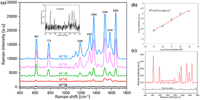 |
| | Fig. 7 Sensitivity of the PNDA substrate. (a) Raman spectra corresponding to the Raman intensities of R6G solutions at varying concentrations from 10−5 to 10−9 M are presented, with the inset displaying the Raman spectrum for the 10−9 M R6G solution. (b) Raman intensities with various concentrations of R6G solutions ranging from 10−5 to 10−9 M at 1364 cm−1 in a logarithmic coordinate. R2 is the correlation coefficient. (c) Raman spectra obtained from 10−7 M R6G absorbed on PNDA (red line) and 10−2 M R6G absorbed on glass (black line); the data of black lines has been amplified by a factor of 5 for clarity. | |
With the aim of estimating the SERS activity, we determined the enhancement factor (EF) of the PNDA substrate according to the following equation:37
where
IS and
IR are the Raman intensities corresponding to the R6G analytes at 1364 cm
−1 acquired from the PNDA substrate and the glass slide, respectively, and
CS and
CR are the molar concentration of R6G analytes absorbed on the above two substrates. From the Raman spectra shown in
Fig. 7(c), we determined that the EF is about 6.7 × 10
6, suggesting a remarkable SERS activity of the PNDA substrate.
3.2.3. Uniformity of the PNDA substrate.
Uniformity of the SERS substrate plays an important role in the practical applications. To estimate the uniformity of the PNDA substrate, Raman spectra of 10−5 M R6G were obtained at fifteen different sites randomly selected on the PNDA substrate. As can be seen in Fig. 8(a), the fifteen Raman spectra obtained at different sites are almost identical, demonstrating splendid uniformity of the PNDA substrate. Furthermore, we selected two characteristic Raman peaks of 10−5 M R6G at 611 cm−1 and 1652 cm−1. We then extracted the corresponding Raman intensities from fifteen different positions as shown in Fig. 8(a) and plotted histograms, which are presented in Fig. 8(b) and (c). We determined that the RSD of the two typical Raman peaks are approximately 6.5% at 611 cm−1 and 8.3% at 1652 cm−1, facilitating the possibility of practical applications of the PNDA structure. This excellent uniformity primarily originates from the ordered PS microsphere array template and UTAAO mask.
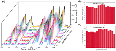 |
| | Fig. 8 (a) Raman spectra of fifteen random positions corresponding to 10−5 M R6G absorbed on the PNDA substrate. Histograms of typical peak intensities at (b) 611 cm−1 and (c) 1652 cm−1 related to 10−5 M R6G absorbed on the PNDA substrate. The data are obtained from the spectra in (a). | |
3.3. Versatility of the PNDA substrate
We demonstrated that PNDA can work not only as a SERS substrate for R6G molecules but also for versatile probe molecules. CV is used in fish farming because it is bactericidal and antiparasitic as well as toxic and teratogenetic43 and thus harmful to human health; therefore, it is meaningful to detect the presence of CV. Fig. 9(a) shows the Raman spectra corresponding to Raman intensities with a variety of CV solution concentrations (from 10−5 to 10−8 M) tested using PNDA substrates, which were soaked in these CV solutions for 2 h and dried using nitrogen gas. When CV concentrations slowly decrease, the Raman intensities gradually decrease as well. The inset of Fig. 9(a) is the Raman spectrum with 10−8 M CV, which indicates that the spectrum remains distinguishable. Furthermore, Fig. 9(b) demonstrates the Raman intensities spectra with diverse concentrations of CV solutions, which ranges from 10−5 to 10−8 M at 1174 cm−1, and shows splendid linear correlation, and the correlation coefficient is 0.952 in the logarithmic coordinate. The results demonstrate that the PNDA structure can be used for the quantitative detection of contaminants in water.
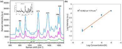 |
| | Fig. 9 (a) Raman spectra corresponding to Raman intensities with various concentrations of CV solutions, ranging from 10−5 to 10−8 M, tested by PNDA substrates, with the inset featuring the Raman spectrum for 10−8 M CV. (b) Raman intensity spectra observed at 1174 cm−1 for varying concentrations of CV solutions, spanning from 10−5 to 10−8 M, displayed on a logarithmic coordinate. R2 is the correlation coefficient. | |
4. Conclusions
We demonstrated a facile construction procedure based on the self-assembled PS microsphere template and UTAAO mask with a thin film deposition technique to fabricate a large-area PNDA structure. Owing to the prominent enhancement of electric field at the cracks and gaps between adjacent island structures, the optimized PNDA substrate exhibited prominent SERS property with high sensitivity (EF = 6.7 × 10⁶) and uniformity (RSD = 6.5% and 8.3%) for measuring R6G analytes. Moreover, the PNDA substrate was demonstrated to effectively detect crystal violet (CV) molecules, known as a hazardous pollutant in water, exhibiting robust SERS sensitivity and a strong linear correlation between the Raman signal and concentration levels. Results indicate that the PNDA substrate can be potentially applied for the development of high-property SERS technique aimed at accurately identifying trace pollutants in an aquatic environment.
Data availability
All data supporting the findings of this study are presented in the article and ESI.† Additional data are available from the corresponding author upon reasonable request.
Conflicts of interest
The authors declare no competing financial interest.
Acknowledgements
This work is supported by the National Key Research and Development Program of China (2023YFF0715501; 2023YFF0715502), National Natural Science Foundation of China (U20A20216), and Anhui Provincial Key Research and Development Project (202304a05020009). Nanofabrication and SEM characterizations were carried out at the USTC Center for Micro and Nanoscale Research and Fabrication.
References
- F. Lu, L. M. Li, K. Shen, Y. Y. Qian, P. F. Zhang, Y. Yang, Q. S. Zhu, Y. Huang, C. X. Yan and W. Wei, Microchim. Acta, 2024, 191, 653 CrossRef CAS PubMed.
- C. Y. Song, Y. Liu, X. Y. Jiang, J. J. Zhang, C. Dong, J. X. Li and L. H. Wang, Talanta, 2019, 205, 120137 CAS.
- M. Zhu, J. Y. Gao, Z. Y. Chen, X. Sun, Y. Duan, X. C. Tian, J. Gu, Q. Q. Shi and M. Sun, Microchim. Acta, 2024, 191, 40 CrossRef CAS PubMed.
- Y. B. Wang, H. J. Ni, H. Li, J. Chen, D. Q. Zhang and L. L. Fu, Chem. Eng. J., 2022, 442, 136140 CrossRef CAS.
- Z. H. Li, K. H. Han, A. X. Zhang, T. Wang, Z. L. Yan, Z. Ding, Y. H. Shen, M. F. Zhang and W. Zhang, Talanta, 2024, 266, 125070 CrossRef CAS PubMed.
- T. T. Zhang, L. Zhang, S. Y. Wu, G. Y. Wang, X. H. Huang, W. H. Li, C. Liu, Z. Kong, J. S. Li and R. Lu, J. Agric. Food Chem., 2024, 72, 865–873 CrossRef CAS PubMed.
- J. Meng, S. H. Qin, L. Zhang and L. B. Yang, Appl. Surf. Sci., 2016, 366, 181–186 CrossRef CAS.
- X. J. Li, L. J. Li, Y. Z. Wang, X. H. Hao, C. Z. Wang, Z. S. Yang and H. F. Li, Spectrochim. Acta, Part A, 2023, 299, 122877 CrossRef CAS PubMed.
- X. Y. Shao, Q. Zhao, J. Y. Xia, M. X. Xie, Q. Z. Li, Y. Q. Tang, X. F. Gu, X. F. Ning, S. S. Geng, J. Fu and S. Tian, Talanta, 2024, 274, 125989 CrossRef CAS PubMed.
- Q. Z. Wang, Y. J. Zhao, T. Bu, X. Wang, Z. H. Xu, H. Zhangsun and L. Wang, Sens. Actuators, B, 2022, 352, 131025 CrossRef CAS.
- Q. Chu, W. Wang, S. Guo, E. Park, S. Jin, Y. Park, L. Chen, Y. C. Liu and Y. M. Jung, ACS Appl. Mater. Interfaces, 2023, 15, 11304–11313 CrossRef CAS PubMed.
- J. Guo, M. Zhang, Z. Z. Yin, C. S. Ding, P. Chen, W. Gan, H. Yu and Z. Q. Sun, Appl. Surf. Sci., 2022, 592, 153265 CrossRef CAS.
- Y. Jiao, Y. Y. Pan, M. R. Yang, Z. Li, J. Yu, R. Fu, B. Y. Man, C. Zhang and X. F. Zhao, Nanophotonics, 2024, 13(3), 307–318 CrossRef CAS PubMed.
- M. J. Mulvihill, X. Y. Ling, J. Henzie and P. D. Yang, J. Am. Chem. Soc., 2010, 132, 268–274 CrossRef CAS PubMed.
- X. X. Li, X. Lin, X. L. Zhao, H. Y. Wang, Y. Y. Liu, S. Lin, L. Wang and S. L. Cong, Appl. Surf. Sci., 2020, 518, 146217 CrossRef CAS.
- Z. D. Yan, W. Du, L. L. Tu, P. Gu, Z. Huang, P. Zhan, F. X. Liu and Z. L. Wang, J. Raman Spectrosc., 2015, 46, 795–801 CrossRef CAS.
- Y. Q. Liu, L. S. Zhang, X. Liu, Y. Z. Zhang, Y. Z. Yan and Y. Zhao, Spectrochim. Acta, Part A, 2022, 270, 120803 CrossRef CAS PubMed.
- S. S. Yang, G. Q. Liu, L. P. Meng, X. Wang, Y. Xiong, Q. P. Luo and S. J. Feng, Opt. Mater., 2021, 112, 110788 CrossRef CAS.
- W. S. Yue, Z. H. Wang, Y. Yang, L. Q. Chen, A. Syed, K. Wong and X. B. Wang, J. Micromech. Microeng., 2012, 22, 125007 CrossRef.
- N. Chamuah, G. P. Vaidya, A. M. Joseph and P. Nath, Plasmonics, 2017, 12, 1353–1358 CrossRef CAS.
- Y. L. Wang, Z. S. Wang, C. N. Chen, J. Q. Liu, J. X. Lu and N. Lu, Anal. Chem., 2023, 95, 14184–14191 CrossRef CAS PubMed.
- V. Suresh, L. Ding, A. B. Chew and F. L. Yap, ACS Appl. Nano Mater., 2018, 1, 886–893 CrossRef CAS.
- Y. Y. Lin, J. D. Liao, Y. H. Ju, C. W. Chang and A. L. Shiau, Nanotechnology, 2011, 22, 185308 CrossRef PubMed.
- X. Q. Zhang, W. J. Salcedo, M. M. Rahman and A. G. Brolo, Surf. Sci., 2018, 676, 39–45 CrossRef CAS.
-
Y. Wang, L. T. Dong, M. N. Liu, M. Z. Ouyang, J. Yang and Z. B. Zhang, IEEE International Conference on Manipulation, Manufacturing and Measurement on the Nanoscale, Chengdu, China, 2023, pp. 290–294.
- C. Liu, J. Wu, S. Wang and J. H. Fang, J. Electroanal. Chem., 2022, 909, 116120 CrossRef CAS.
- T. T. Fan, Y. Ke, L. J. Zhang, L. Cai and Z. B. Li, CrystEngComm, 2022, 24, 4764–4771 RSC.
- J. R. Liang, L. Z. Yu, Y. X. Wang, T. Xue, D. Y. Lei, Z. Y. Wang and X. Z. Li, Adv. Opt. Mater., 2022, 10, 2102615 CrossRef CAS.
- S. H. Luo, A. Mancini, E. K. Lian, W. Q. Xu, R. Berte and Y. Li, Nanomaterials, 2022, 12, 3842 CrossRef CAS PubMed.
- Y. J. Xia, M. N. Sun, R. J. Huang, S. Y. Qi, L. Zhang, Y. R. Jia, Z. H. Li, H. L. Xu, M. K. Wang, W. Huang, J. T. Zhang, A. G. Wu and B. Chen, New J. Chem., 2024, 48, 10104 RSC.
- S. S. Yan, C. H. Zhu, A. Y. Wang, J. C. Sun, Y. J. Hang, B. Chen, X. J. Wang, N. Q. Wu, H. B. Tang, L. Y. Wen and G. W. Meng, Adv. Opt. Mater., 2023, 11, 2300508 CrossRef CAS.
- Y. Q. Liu, M. H. Li, L. L. Liang, C. Feng, Y. Z. Zhang, X. Liu and Y. Zhao, Opt. Mater., 2022, 128, 112381 CrossRef CAS.
- J. Ma, W. Liu, Z. Ma, P. S. Song, Y. Q. Zhao, F. H. Yang and X. D. Wang, Nanoscale, 2019, 11, 20194–20198 RSC.
- S. S. Yan, H. B. Tang, J. C. Sun, C. H. Zhu, Q. J. Pan, B. Chen and G. W. Meng, Adv. Opt. Mater., 2024, 12, 2302010 CrossRef CAS.
- M. Kong, Y. Y. Wu, D. D. Men, Q. Q. Ding and H. H. Zhang, RSC Adv., 2023, 13, 36181–36187 RSC.
- K. G. Li, X. Y. Tang, H. Y. Wang, M. H. Huang, G. J. Liu, Y. Zhou, W. X. Huang, Z. W. Zuo and Y. H. Lu, Appl. Surf. Sci., 2023, 613, 156117 CrossRef CAS.
- K. G. Li, X. Y. Tang, H. Y. Wang, M. H. Huang, G. J. Liu, Y. Zhou, W. X. Huang and Z. W. Zuo, Appl. Surf. Sci., 2024, 669, 160544 CrossRef CAS.
- D. Wang, G. C. Xu, X. S. Zhang, H. Y. Gong, L. Jiang, G. L. Sun, Y. Li, G. R. Liu, Y. Li, S. K. Yang and X. Liang, Sens. Actuators, B, 2022, 359, 131512 CrossRef CAS.
- Y. Wang, B. Ai, Z. Y. Wang, Y. D. Guan, G. Xiao and G. Zhang, Appl. Surf. Sci., 2023, 615, 156271 CrossRef CAS.
- K. G. Li, X. Y. Tang, G. J. Liu, J. J. Mi, J. Du, W. X. Huang, Z. W. Zuo and Y. H. Lu, Appl. Surf. Sci., 2021, 570, 151069 CrossRef CAS.
- L. W. Ma, Y. Huang, M. J. Hou, Z. Xie and Z. J. Zhang, Sci. Rep., 2015, 5, 15442 CrossRef CAS PubMed.
- H. Y. Wei and H. Eilers, J. Phys. Chem. Solids, 2009, 70, 459–465 CrossRef CAS.
- X. J. Chen, Q. L. Wang, L. X. Qin, X. X. Liu, S. Z. Kang, T. Y. Zhang and X. Q. Li, Mater. Adv., 2022, 3, 2583 RSC.
|
| This journal is © The Royal Society of Chemistry 2025 |
Click here to see how this site uses Cookies. View our privacy policy here. 
 Open Access Article
 This Open Access Article is licensed under a Creative Commons Attribution-Non Commercial 3.0 Unported Licence
 *b,
Yonghua
Lu
*b,
Yonghua
Lu