
Annealing-free Ohmic contact of β-Ga2O3via nitrogen plasma treatment†
Junghun
Kim
 a,
Hyoung Woo
Kim
a,
Woong
Choi
b,
Jihyun
Kim
b and
Dongryul
Lee
*b
a,
Hyoung Woo
Kim
a,
Woong
Choi
b,
Jihyun
Kim
b and
Dongryul
Lee
*b
aKorea Electrotechnology Research Institute (KERI), Seongsan-gu, Changwon-si, Gyeongsangnam-do 51543, Republic of Korea
bDepartment of Chemical and Biological Engineering, Seoul National University, Seoul 08826, Republic of Korea. E-mail: daecon.lee@snu.ac.kr
First published on 3rd May 2025
Abstract
With the advent of the artificial intelligence era, semiconductor materials with exceptional performance are increasingly in demand. Beta-gallium oxide (β-Ga2O3) is a promising candidate for advanced semiconductor applications; however, its limited contact performance between metal electrodes remains a critical restriction that impedes its full utilization. In this study, high-quality Ohmic contacts were established through a direct nitrogen plasma treatment, effectively preserving the crystallinity of β-Ga2O3 while enhancing its electrical performance. The carrier mobility of β-Ga2O3 reached levels up to 76 cm2 V−1 s−1, approximately four times greater than the previously reported ranges (15–20 cm2 V−1 s−1). The significantly improved on/off ratio (1.7 × 10¹⁰) can suppress the device malfunction due to leakage current and resolve existing structural limitations. The results of our investigation provide insights for the advancement of β-Ga2O3 as a cutting-edge semiconductor material for ultra-low-scale and multi-output integrated circuits.
Introduction
With the emergence of the artificial intelligence (AI) era and the imminent rise of high power processors that include circuits and amplifiers, the extreme miniaturization of circuit patterns, driven by high-density and down-scale demands in modern semiconductors, requires efficient current flowing with circuits in even smaller contact areas.1–3 The foundation for on-device AI networking and high-bandwidth operations lies in achieving high-performance electronic devices, which starts with highly efficient metal via – semiconductor channel contacts.4–6 Despite the potential of a material, if effective signal transmission between the material and the input line is not achieved, latency occurs, thus undermining the fundamental functionality of the circuit.7,8 In this regard, beta-gallium oxide (β-Ga2O3), which is considered as a promising channel material for high-power semiconductors and diverse communication applications, can facilitate a high-performance multi-input/output channel with excellent electron mobility, subthreshold swing (SS), and ideality factor, meeting the need for high-capacity data transfer (in larger GB/s).9–11 However, despite the significant advancements in the study of the electrical properties of β-Ga2O3, research on its contact with metals (via or electrode) remains limited. Without rapid thermal annealing (RTA), the formation of contacts between β-Ga2O3 and metals has rarely been successful.12 Even with the RTA process, the Schottky barrier between the metal and β-Ga2O3 contact is typically high, and the contact resistance remains elevated, often requiring additional thermal treatment or high-concentration doping in the contact area.13,14 The RTA process can lead to challenges such as metal vaporization of the electrode and degradation from the dopant or oxygen penetration at the interface. These issues impose significant constraints, limiting the contact formation with β-Ga2O3 in the front-end process, as such contact formation is not feasible during the middle- and back-end process.15 Therefore, research on low-temperature, high-efficiency contact improvements is essential to unlock the full potential of on-device applications with β-Ga2O3. For the extensive application of β-Ga2O3 in devices, the conventional thermal treatment approach to enhance contact characteristics has limitations for both front-end and back-end process integration. Annealing-related issues such as metal vaporization (e.g., Ti) are significant, and achieving a process integration margin is possible when contact processes perform well in integrated circuits. To establish stable performance in small areas without thermal treatment, further research is necessary.16β-Ga2O3, with its ultra-wide bandgap of 4.8 eV and a high breakdown electric field of 8 MV cm−1, is an excellent material applied in various electronic devices like high-performance Schottky barrier diodes (SBDs) and metal-oxide semiconductor field-effect transistors (MOSFETs).17–19 Recently, epitaxy and chemical vapor deposition (CVD) methods, which support commercialization, have enabled high-quality large-area growth of β-Ga2O3.20–22 Its high power allowance and current capacity make it suitable for a wide range of applications, i.e., from high to low power.23 β-Ga2O3 possesses fine radiation hardness, eliminating the need for extra radiation passivation and optimization, which are essential for semiconductor applications in the aerospace industry.24,25 β-Ga2O3 is highly suitable as an on-chip channel material capable of handling vast amounts of data transfer, signal processing, and computation required by AI semiconductor devices. From the perspective of device reliability, which is essential for repetitive calculations and data operations, β-Ga2O3 demonstrates excellent bias temperature instability (BTI) reliability and high breakdown voltage, thus providing stable operational tolerance even under extreme external conditions compared to traditional silicon. Although a simple deposition process can enable contact formation with metals without mismatch issues, additional contact formation processes are necessary to enhance performance.
This study proposes high-quality contact formation in β-Ga2O3via straightforward nitrogen (N2) plasma treatment at room temperature, without the need for thermal annealing. The nitrogen substitution mechanism effectively mitigates challenges associated with thermal treatment, while enabling the formation of complete contact. The nitrogen plasma-treated β-Ga2O3 nanoFETs with a small contact area exhibit high on/off ratios, high field-effect mobility, and low contact resistance. Through enhanced, high-quality contacts in small areas, β-Ga2O3 can emerge as an ideal on-device semiconductor material for next-generation multi-output/high-density data circuits.
Experimental details
A schematic of the β-Ga2O3 TLM device is shown in Fig. 1a. The β-Ga2O3 Sn-doped (001) surface orientation β-Ga2O3 substrates (Novel Crystal Technology, Japan) with an electron concentration of approximately 3 × 1018 cm−3 were cleaned with a sequential solvent cleaning process prior to device fabrication. The TLM device patterns were defined by standard photolithography, and N2 plasma treatment was performed at room temperature at a flow rate of 10 sccm and an applied radio frequency power of 100 W for 30 s, using a plasma cleaner (Tergeo, Pie Scientific). The TLM electrodes were deposited on top of the N2 plasma-treated β-Ga2O3 with e-beam evaporated Ti/Au (50/100 nm). To examine the feasibility of N2 plasma treatment on a small contact area, a β-Ga2O3 nanoFET was fabricated using a mechanically exfoliated β-Ga2O3 flake. The β-Ga2O3 flake was dry-transferred onto SiO2/p+-Si (300 nm/500 μm) with a back gate using transparent gel films (Gelpak) at 40 °C. The contact areas were defined by e-beam lithography followed by e-beam evaporation of a Ti/Au (50/100 nm) Ohmic electrode after N2 plasma treatment. | ||
| Fig. 1 (a) Schematic of the transfer-length method (TLM) pattern fabricated on the β-Ga2O3 substrate with N2 plasma treatment. (b) and (c) the I–V characteristics of the β-Ga2O3 TLM devices without and with N2 plasma treatment, respectively. | ||
Micro-Raman spectroscopy was employed to investigate the changes in the crystalline properties after the plasma treatment with a 532 nm diode-pumped solid-state laser (Omicron) under backscattering geometry. The differences in the thickness and surface roughness after the plasma treatment were measured using an AFM (NX10, Park System). XPS (Nexsa, ThermoFisher Scientific), with an Al Kα monochromator as the X-ray source, was performed to examine the changes of the chemical surface bonding states after the plasma treatment. The XPS data were calibrated using the reference C 1s peak (284.8 eV). Cross-sectional HR-TEM (JEM-ARM200F, JEOL) and EDS profiling were performed to investigate the structure of samples before and after the plasma treatment, and the specimens were prepared using the focused-ion beam technique (Helios 5UX). The electrical properties of the TLM and FET devices were analyzed using a semiconductor parameter analyzer (Agilent 4156B and 4155C, respectively).
Results and discussion
Fig. 1a shows the fabrication process of the designed transfer-length method (TLM) pattern on N2 plasma-treated β-Ga2O3 substrates. The TLM pattern was designed with lengths of 5, 10, 15, 20, 25, and 30 μm between the electrodes. The pristine sample, used as a control, was fabricated by depositing only Ti/Au (50/100 nm) metal for contact without any additional processes. In contrast, the modified sample underwent N2 plasma treatment at 100 W and a flow rate of 10 sccm for 30 s after photolithography for metal patterning, followed by simultaneous metal deposition as with the pristine sample. RF power conditions of 50–80 W resulted in inconsistent or incomplete Ohmic contact formation, and power levels of 120–150 W did not yield further improvement in electrical performance compared to that under 100 W conditions. Based on a systematic investigation of RF power conditions, 100 W was selected as the optimal plasma treatment condition. Fig. 1b and c show the current–voltage (I–V) characteristics of the TLM pattern without and with N2 plasma treatment, respectively. The pristine sample exhibited Schottky behavior, achieving a current of 0.69 mA mm−1 at 0.1 V with a length of 30 μm, whereas after plasma treatment, an Ohmic contact was formed, with the current level improved by approximately two orders of magnitude. Fig. S1 (ESI†) shows the fitted data for calculating contact resistance, with the plasma-treated sample demonstrating a specific contact resistance of 2.66 × 10⁻⁴ Ω cm2. Ultra-wide bandgap materials such as β-Ga2O3 are prone to Fermi level pinning due to surface states or defects, making Ohmic contact formation challenging. Additionally, β-Ga2O3 contains native oxygen vacancies, which can cause instability in electrical properties.26,27 Given the analogous atomic radius of nitrogen and oxygen, the incorporation or substitution of nitrogen into oxygen vacancies presents a viable and promising approach.28,29 The passivation effect on the surface from N2 plasma treatment possibly contributed to the reduction of oxygen vacancies and the formation of a clear metal/semiconductor interface, achieving an Ohmic contact.30To examine surface changes triggered by the ion bombardment from direct N2 plasma, atomic force microscopy (AFM) measurements were conducted to assess thickness and the root mean square (RMS) roughness. Fig. 2a shows the thickness profile of the β-Ga2O3 flake before and after N2 plasma treatment. The thickness before plasma treatment showed 271 nm, and even after plasma treatment, the identical thickness was maintained, confirming that no etching occurred due to ion bombardment. The RMS surface roughness of the β-Ga2O3 flake decreased from 1 nm to 0.7 nm, suggesting that smoothing was achieved through vacancy passivation rather than surface etching. Previous studies have reported reductions in contact resistance by forming oxygen vacancies through Ar-based reactive ion etching (RIE). The main difference lies in the mechanism of defect passivation through N2 plasma treatment, where RMS roughness decreases, as opposed to defect generation in Ar-based RIE, which results in a sharp increase in RMS roughness.31 Defect generation through etching is challenging to control and can cause undesired damage to the device, whereas defect passivation can create a suitable surface state for Ohmic formation without causing damage. Fig. 2b shows the changes in the Raman shift before and after N2 plasma treatment. The Raman peaks of pristine β-Ga2O3 (black line) show 10 vibrational modes located at 111.6, 169.8, 200, 320.5, 347, 417.3, 477.6, 630, 652, and 766 cm−1, which are typical Raman vibrational modes of β-Ga2O3 and in good agreement with the existing literature.32 The Raman-active vibrational modes of β-Ga2O3 can be classified into high-frequency modes (700–500 cm−1) associated with the stretching and bending of GaO4 tetrahedra, mid-frequency modes (480–310 cm−1) related to the deformation of GaO6 octahedra, and low-frequency modes (below 200 cm−1) corresponding to the vibrations and translations of GaO4 tetrahedra and GaO6 octahedra chains. After N2 plasma treatment, the same 10 vibrational modes were observed, and no intensity changes or new peaks appeared, thus confirming that N2 plasma treatment did not affect the crystallinity of β-Ga2O3. However, the 320 and 347 cm−1 peaks in the mid-frequency range, corresponding to A(4)g and A(5)g, were blue-shifted to 321.7 and 348.7 cm−1. The A(4)g and A(5)g phonon modes are associated with the bending vibration mode, and the observed blue-shift is attributed to changes in the bond angles within β-Ga2O30.33 Considering the reference, this blue-shift is likely due to the reduction of point defects like oxygen vacancies and the substitution of larger N atoms with O atoms, which increases bond strength and shifts the Raman peaks.34
 | ||
| Fig. 2 (a) Atomic force microscope (AFM) height profile and (b) Raman spectra of the β-Ga2O3 obtained before and after N2 plasma treatment. (c) Comparison of the Raman spectra of the mid-frequency modes, shown before (black line) and after (red line) N2 plasma treatment. | ||
X-ray photoelectron spectroscopy (XPS) analysis was conducted to examine the surface chemical bonding states of β-Ga2O3 after N2 plasma treatment. Fig. 3 shows the XPS data for the changes in the O 1s spectra of β-Ga2O3 samples treated with plasma at bias powers of pristine, 50, 100, and 150 W. The O 1s spectrum peak of the β-Ga2O3 film can be divided into three peaks: peak O(I) (530.7 eV) originates from Ga–O bonding, peak O(II) (531.3 eV) is attributed to O2− ions in oxygen-deficient regions, and peak O(III) (532.4 eV) is related to chemisorbed hydroxyl and carbonate species.35,36 The Gaussian peak O(II), related to oxygen deficiency, tends to decrease as plasma treatment power increases. This result indicates that N2 plasma treatment is sufficient to achieve effective surface passivation of the β-Ga2O3 surface. Meanwhile, the Raman spectra shown in Fig. 2 confirm the absence of detectable lattice damage after plasma treatment. These findings suggest that the plasma-induced passivation occurs without introducing structural defects into the β-Ga2O3 lattice. Additionally, by calculating the area ratio of O(II)/(O(I) + O(II)), the trend in oxygen-related defects according to N2 plasma bias power was confirmed. For plasma bias powers of pristine, 50, 100, and 150 W, and the area ratios of O(II)/(O(I) + O(II)) decreased progressively to 42.39%, 25.08%, 24.26%, and 22.58%, respectively. This indicates that oxygen vacancies are passivated by N2 plasma, resulting in a reduction of these defects. Furthermore, in the XPS spectrum of Ga 2p, the Ga 2p3/2 and Ga 2p1/2 peaks tend to shift to lower binding energies as plasma power increases, indicating the formation of Ga–N bonds (Fig. S2, ESI†).37,38
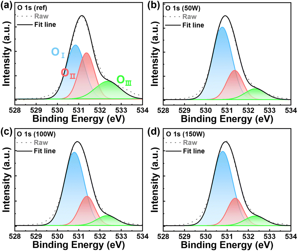 | ||
| Fig. 3 X-ray photoelectron spectroscopy (XPS) spectra of the O 1s peak of plasma treated β-Ga2O3 substrates with bias powers of (a) pristine, (b) 50 W, (c) 100 W, and (d) 150 W. | ||
To investigate the effects of N2 plasma treatment on the β-Ga2O3 lattice and the interface with metal (Ti), high-resolution transmission electron microscope (HR-TEM) and energy dispersive spectroscopy (EDS) analyses were conducted. Fig. 4a shows a TEM image of the overall area at low magnification. The blue-dashed square marks the N2 plasma-treated area, while the green dashed square indicates the untreated pristine area. In the plasma-treated region, a thin amorphous oxide layer (marked in white) is visible, whereas this layer is not observed in the pristine area. Fig. S3 (ESI†) shows a TEM image of a β-Ga2O3 sample with only metal deposition, without plasma treatment. An amorphous oxide layer was also formed in the pristine sample, which was noticeably thinner compared to the plasma-treated sample. Fig. 4b and c show high-magnification TEM images of the plasma-treated and untreated areas, respectively. Fig. 4b presents the interface between Ti and N2 plasma-treated β-Ga2O3, in which the 3–4 layers of β-Ga2O3 located beneath the amorphous Ti maintain the original lattice structure. This structure is consistent with that of the untreated channel shown in Fig. 4c. However, one layer at the interface between Ti and β-Ga2O3 appears partially blurred, which is attributed to the formation of TiOX resulting from the interaction between Ti and the O atoms in the passivated Ga2O3 layer during the Ti metal deposition process. To investigate the composition of the slightly blurred interfacial layer and the overlying Ti area, an EDS line profile was conducted (Fig. 4d). In Fig. 4d, the amorphous layer formed at the β-Ga2O3 interface appears in black and consists of Ti and O atoms, forming TiOX. The formed TiOX layer (approximately 3.6–3.9 eV for Ti2O3) has a relatively lower bandgap than β-Ga2O3 (approximately 4.8 eV), facilitating electron transport and aiding in Ohmic contact formation.39 Additionally, a reduction in oxygen at the metal/semiconductor interface was observed, without diffusion of Ti atoms. This is likely because N2 plasma treatment causes O and N substitution on the β-Ga2O3 surface, forming an oxygen layer that easily reacts with Ti. Fig. 4e–h shows EDS mapping images of N2 plasma treated β-Ga2O3 regarding base, Ga, O, and Ti atoms, respectively. In the EDS mapping image of O atoms shown in Fig. 4g, oxygen has evidently disappeared from the β-Ga2O3 interface, and, consistent with the EDS line profile results, out-diffused into the Ti region. Fig. S4 (ESI†) shows the EDS mapping of pristine (untreated) β-Ga2O3. In Fig. S4 (ESI†), oxygen does not out-diffuse even after metal deposition, verifying that the formation of TiOX is due to N2 plasma treatment.
 | ||
| Fig. 4 Cross-sectional transmission electron microscopy (TEM) images of the (a) β-Ga2O3 structure showing both plasma-treated and untreated area, (b) interface of Ti/plasma-treated β-Ga2O3 (blue dash square), and (c) carbon-coated β-Ga2O3 (green dash square). (d) Energy dispersive spectroscopy (EDS) line profile across the interface between Ti and plasma-treated β-Ga2O3, along with the corresponding count per second. (e) High magnification TEM image of the interfacial region, where a TiOX layer is formed. (f)–(h) EDS mapping of gallium, oxygen, and titanium corresponding to the region shown in (e). | ||
Fig. 5 shows the electrical characteristics of a β-Ga2O3 MOSFET fabricated using the N2 plasma treatment method. The β-Ga2O3 device was fabricated using a flake obtained by mechanical exfoliation. As shown in Fig. 5a, N2 plasma treatment was applied only to the contact area of the exfoliated flake without annealing, creating a small contact area. The transfer and output characteristics of N2 plasma-treated β-Ga2O3 MOSFET are shown in Fig. 5b and 5c, respectively. An extremely high on/off ratio of 1.7 × 10¹⁰ and a high field-effect mobility of 76 cm2 V−1 s−1 were achieved, along with a low contact resistance of 13.1 kΩ μm calculated using the Y-function method. In modern semiconductor scaling down processes, the gate-induced drain leakage current (GIDL) poses a significant risk to the stable operation of transistors. This device maintains a leakage current level at the 100 fA level while achieving an extremely high on/off ratio of 1.7 × 10¹⁰ at VDS = +20 V, and 8.8 × 10⁹ at VDS = +5 V. Considering that the recommended and conventional value for existing silicon devices is 106, and for β-Ga2O3 it does not exceed 108, this demonstrates exceptionally high device stability.40,41 In conventional semiconductor physics, the limited on/off ratio margin compels structures such as gate-all-around and buried channel array transistors with constructing heterojunction gates (like TiN and poly-Si) or creating deep shallow trenches. However, the record-high on/off ratio in our device eliminates the need for such impractical measures. Even in ultra-low-scale integration arrays, the high on-current can effectively prevent deterioration caused by GIDL characteristics caused by adjacent rows.
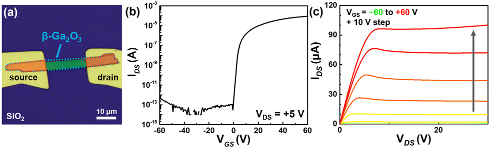 | ||
| Fig. 5 Optical and electrical properties of the N2 plasma-treated β-Ga2O3 field-effect transistor (FET). (a) Optical microscopy images of the fabricated β-Ga2O3 device, (b) VGS–IDS transfer curve, and (c) VDS–IDS output characteristics. | ||
As shown in Fig. S5 and Table S1 (ESI†), the effect of N2 plasma treatment on contact behavior was further evaluated under elevated temperature conditions. Consistent with typical temperature-dependent FET characteristics, the threshold voltage decreased, subthreshold swing increased, and both on-current and off-current increased with rising temperature. The improved contact behavior achieved through nitrogen plasma treatment appears to be largely independent of the thermal degradation of the channel itself, maintaining stable contact properties and sustaining increased on-current levels even under high-temperature operation. In addition, to evaluate the effect of additional annealing on the plasma-induced contact, transfer characteristics measured before and after rapid thermal annealing at 500 °C exhibited no significant changes (Fig. S6, ESI†). This indicates that the TiOX layer formed on the nitrogen plasma-treated surface was already sufficient to achieve an Ohmic contact, and that additional TiOX generated during annealing did not further enhance contact behavior.
Unlike conventional nitrogen ion implantation, which involves high-energy ion beams and thermal annealing, the nitrogen plasma treatment used in this study was performed at room temperature with low RF power (100 W), minimizing the possibility of lattice damage. Given the shallow penetration depth, the effect is limited to surface-level modifications such as trap passivation and oxygen vacancy compensation. The observed improvement in contact behavior is therefore attributed to surface state engineering rather than bulk doping or defect-induced charge trapping. This mechanism is further supported by AFM analysis and annealing results indicating stable and low-resistance contact formation.
Furthermore, the field-effect mobility, which is more than four times higher compared to that in conventional β-Ga2O3 devices, appears to result from the high carrier concentration in the contact area and low trap-induced scattering from passivated contact surface by N2 plasma treatment.42,43 This suggests that the previously achieved low mobility in β-Ga2O3 is attributed to poor contact quality rather than the intrinsic potential of β-Ga2O3. High mobility directly correlates with lower latency and faster operating speed, allowing the transmission of various signals with lower power, thereby expanding the range of electronic applications for β-Ga2O3. Despite the small contact area, the excellent performance of the device offers significant advantages in achieving larger margins in processes beyond contact formation in advanced low-scale applications. Additionally, the annealing-free process is highly compatible with various manufacturing processes, greatly enhancing process flexibility. The findings of our study can contribute to industrializing high-performance β-Ga2O3-based devices.
Conclusions
In summary, we proposed a novel annealing-free N2 plasma treatment for achieving Ohmic contacts in β-Ga2O3 devices. This straightforward approach effectively reduced the contact resistance to 13.1 kΩ μm through a defect passivation mechanism. XPS analysis confirmed the modification of Ga–O and oxygen-related bonds induced by the N2 plasma treatment, Raman spectroscopy demonstrated that the crystalline quality of the treated region was well preserved without any significant degradation. β-Ga2O3 nanosheet FETs incorporating the N2 plasma-treated contacts exhibited an on/off ratio of 1.7 × 10¹⁰ and a field-effect mobility of 76 cm2 V−1 s−1. The proposed highly effective and scalable approach to reducing contact resistance enables the full exploitation of the inherent potential of β-Ga2O3-based devices, optimizing their performance and enhancing their operational reliability.Author contributions
Junghun Kim – investigation, visualization, formal analysis, writing – original draft. Hyoungwoo Kim – project administration, methodology. Woong Choi – formal analysis, methodology. Jihyun Kim – validation, resources. Dongryul Lee – conceptualization, supervision, data curation, writing – review & editing, and project administration.Data availability
The data supporting the primary research of this article have been included within the main manuscript and as part of the ESI.† All referenced data are publicly available in the cited literature.Conflicts of interest
There are no conflicts to declare.Acknowledgements
This research was supported by the Korea Research Institute for Defense Technology Planning and Advancement (KRIT) grant funded by the Defense Acquisition Program Administration (DAPA) (KRIT-CT-22-046) and the K-Sensor Development Program (No. RS-2022-00154729), funded by the Ministry of Trade, Industry and Energy (MOTIE, Korea)Notes and references
- C. X. Xue, Y. C. Chiu, T. W. Liu, T. Y. Huang, J. S. Liu, T. W. Chang, H. Y. Kao, J. H. Wang, S. Y. Wei, C. Y. Lee, S. P. Huang, J. M. Hung, S. H. Teng, W. C. Wei, Y. R. Chen, T. H. Hsu, Y. K. Chen, Y. C. Lo, T. H. Wen, C. C. Lo, R. S. Liu, C. C. Hsieh, K. T. Tang, M. S. Ho, C. Y. Su, C. C. Chou, Y. D. Chih and M. F. Chang, Nat. Electron., 2020, 4, 81–90 CrossRef
.
- J. Lee, P. Asenov, R. Rhyner, E. Kao, S. M. Amoroso, A. R. Brown, X. W. Lin and V. Moroz, IEEE Trans. Electron Devices, 2024, 71, 1893–1899 Search PubMed
- L. Ye, Z. Wang, T. Jia, Y. Ma, L. Shen, Y. Zhang, H. Li, P. Chen, M. Wu, Y. Liu, Y. Jing, H. Zhang and R. Huang, Sci. China Inf. Sci., 2023, 66, 200407 CrossRef
- D. D. Sharma, R. Blankenship and D. Berger, ACM Comput. Surv., 2024, 56, 1–37 CrossRef
- A. Liu, X. Zhang, Z. Liu, Y. Li, X. Peng, X. Li, Y. Qin, C. Hu, Y. Qiu, H. Jiang, Y. Wang, Y. Li, J. Tang, J. Liu, H. Guo, T. Deng, S. Peng, H. Tian and T. L. Ren, Nano-Micro Lett., 2024, 16, 119 CrossRef
- S. Batool, M. Idrees, S. T. Han, V. A. L. Roy and Y. Zhou, Small, 2023, 19, 2206550 CrossRef CAS PubMed
- Z. Zhou, J. Wei, Y. Luo, K. A. Clark, E. Sillekens, C. Deakin, R. Sohanpal, R. Slavík and Z. Liu, Nat. Electron., 2023, 6, 694–702 CrossRef
- S. Sadulla, Prog. Electron. Commun. Eng., 2024, 1, 13–18 Search PubMed
- Y. Zhang, R. Zhu, W. Huo, H. Liang and Z. Mei, Nano Lett., 2024, 24, 14398–14404 CrossRef CAS
- J. H. Kim, H. J. Lee, H. J. Kim, J. Choi, J. H. Oh, D. C. Choi, J. Byun, S. E. Ahn and S. N. Lee, Adv. Electron. Mater., 2024, 10, 2300863 CrossRef CAS
- S. Sun, C. Wang, S. Alghamdi, H. Zhou, Y. Hao and J. Zhang, Adv. Electron. Mater., 2024, 2300844 Search PubMed
- S. Wu, Z. Liu, H. Yang and Y. Wang, Crystals, 2023, 13, 1045 CrossRef CAS
- K. Tetzner, A. Thies, P. Seyidov, T. S. Chou, J. Rehm, I. Ostermay, Z. Galazka, A. Fiedler, A. Popp, J. Würfl and O. Hilt, J. Vac. Sci. Technol., A, 2023, 41, 043102 CrossRef CAS
- L. Q. Zhang, W. Q. Miao, X. L. Wu, J. Y. Ding, S. Y. Qin, J. J. Liu, Y. T. Tian, Z. Y. Wu, Y. Zhang, Q. Xing and P. F. Wang, Inorganics, 2023, 11, 397 CrossRef CAS
- Z. Yu, X. Yang, X. Zhao, Y. Li, S. He and Y. Wang, J. Vac. Sci. Technol., B, 2024, 42, 062202 CrossRef CAS
- S. G. Jung, J. K. Kim and H. Y. Yu, IEEE Trans. Electron Devices, 2022, 69, 930–935 CAS
- W. Li, D. Saraswat, Y. Long, K. Nomoto, D. Jena and H. G. Xing, Appl. Phys. Lett., 2020, 116, 192101 CrossRef CAS
- K. Zeng, A. Vaidya and U. Singisetti, Appl. Phys. Express, 2019, 12, 081003 CrossRef CAS
- S. J. Pearton, F. Ren, M. Tadjer and J. Kim, J. Appl. Phys., 2018, 124, 220901 CrossRef
- S. B. Anooz, R. Grüneberg, C. Wouters, R. Schewski, M. Albrecht, A. Fiedler, K. Irmscher, Z. Galazka, W. Miller, G. Wagner, J. Schwarzkopf and A. Popp, Appl. Phys. Lett., 2020, 116, 182106 CrossRef
- M. J. Tadjer, F. Alema, A. Osinsky, M. A. Mastro, N. Nepal, J. M. Woodward, R. L. Myers-Ward, E. R. Glaser, J. A. Freitas, A. G. Jacobs, J. C. Gallagher, A. L. Mock, D. J. Pennachio, J. Hajzus, M. Ebrish, T. J. Anderson, K. D. Hobart, J. K. Hite and C. R. Eddy, J. Phys. D, 2021, 54, 034005 CrossRef CAS
- G. Seryogin, F. Alema, N. Valente, H. Fu, E. Steinbrunner, A. T. Neal, S. Mou, A. Fine and A. Osinsky, Appl. Phys. Lett., 2020, 117, 262101 CrossRef CAS
- M. A. Mastro, A. Kuramata, J. Calkins, J. Kim, F. Ren and S. J. Pearton, ECS J. Solid State Sci. Technol., 2017, 6, 356–359 CrossRef
- A. Azarov, J. G. Fernández, J. Zhao, F. Djurabekova, H. He, R. He, Ø. Prytz, L. Vines, U. Bektas, P. Chekhonin, N. Klingner, G. Hlawacek and A. Kuznetsov, Nat. Commun., 2023, 14, 4855 CrossRef CAS PubMed
- J. Kim, S. J. Pearton, C. Fares, J. Yang, F. Ren, S. Kim and A. Y. Polyakov, J. Mater. Chem. C, 2019, 7, 10–24 RSC
- J. B. Varley, J. R. Weber, A. Janotti and C. G. Van de Walle, Appl. Phys. Lett., 2010, 97, 142106 CrossRef
- M. D. McCluskey, J. Appl. Phys., 2020, 127, 101101 CrossRef CAS
- G. Li, A. Abliz, L. Xu, N. André, X. Liu, Y. Zeng, D. Flandre and L. Liao, Appl. Phys. Lett., 2018, 112, 253504 CrossRef
- H. Wang, H. Zhan, Y. Zhou, Y. Wu, X. Chen, H. Wang and J. Kang, Nanoscale, 2016, 8, 4381–4386 RSC
- K. M. Niang, B. C. Bayer, J. C. Meyer and A. J. Flewitt, Appl. Phys. Lett., 2017, 111, 122109 CrossRef
- P. Kachhawa, A. K. Jain and N. Chaturvedi, Phys. Status Solidi A, 2023, 220, 2200722 CrossRef CAS
- C. Kranert, C. Sturm, R. Schmidt-Grund and M. Grundmann, Sci. Rep., 2016, 6, 35964 CrossRef CAS
- K. Zhang, Z. Xu, S. Zhang, H. Wang, H. Cheng, J. Hao, J. Wu and F. Fang, Phys. B, 2021, 600, 412624 CrossRef CAS
- R. Rao, A. M. Rao, B. Xu, J. Dong, S. Sharma and M. K. Sunkara, J. Appl. Phys., 2005, 98, 094312 CrossRef
- X. Hou, X. Zhao, Y. Zhang, Z. Zhang, Y. Liu, Y. Qin, P. Tan, C. Chen, S. Yu, M. Ding, G. Xu, Q. Hu and S. Long, Adv. Mater., 2022, 34, 2106923 Search PubMed
- L. X. Qian, Z. H. Wu, Y. Y. Zhang, P. T. Lai, X. Z. Liu and Y. R. Li, ACS Photonics, 2017, 4, 2203–2211 CrossRef CAS
- J. Wang, X. Ji, S. Qi, Z. Li, Z. Yan, M. Li, X. Yan, A. Zhong, C. Lu, X. Qi and P. Li, J. Mater. Chem. C, 2023, 11, 6202–6211 RSC
- Y. Zhang, X. Chen, Y. Xu, H. Gong, Y. Yang, F. F. Ren, B. Liu, S. Gu, R. Zhang and J. Ye, ACS Appl. Electron. Mater., 2020, 2, 808–816 CrossRef CAS
- J. Bae, H. Y. Kim and J. Kim, ECS J. Solid State Sci. Technol., 2017, 6, 3045–3048 CrossRef
- N. Moser, J. McCandless, A. Crespo, K. Leedy, A. Green, A. Neal, S. Mou, E. Ahmadi, J. Speck, K. Chabak, N. Peixoto and G. Jessen, IEEE Electron Dev. Lett., 2017, 38, 775–778 CAS
- J. Kim, M. A. Mastro, M. J. Tadjer and J. Kim, ACS Appl. Mater. Interfaces, 2018, 10, 29724–29729 Search PubMed
- J. Kim, H. Kim, I. Kang, J. Kim, S. Ko, J. Bae and J. Kim, J. Mater. Chem. C, 2024, 12, 6193–6200 RSC
- H. Zhou, M. Si, S. Alghamdi, G. Qiu, L. Yang and P. D. Ye, IEEE Electron. Dev. Lett., 2017, 38, 103–106 Search PubMed
Footnote |
| † Electronic supplementary information (ESI) available: Calculating contact resistance, XPS spectra of Ga 2p peaks, and TEM and EDS mapping of β-Ga2O3 without plasma treatment (Fig. S1–S4). See DOI: https://doi.org/10.1039/d5tc00129c |
| This journal is © The Royal Society of Chemistry 2025 |