
 Open Access Article
 This Open Access Article is licensed under a Creative Commons Attribution-Non Commercial 3.0 Unported Licence
Flexible transparent layered metal oxides for organic devices†
Tao
Zhang
a,
Peicheng
Li
b,
Nan
Chen
c,
Jiale
Su
 a,
Zhenxin
Yang
d,
Dengke
Wang
a,
Nan
Jiang
a,
Changsheng
Shi
a,
Qiang
Zhu
a,
Hongyu
Yu
c and
Zheng-Hong
Lu
*ab
a,
Zhenxin
Yang
d,
Dengke
Wang
a,
Nan
Jiang
a,
Changsheng
Shi
a,
Qiang
Zhu
a,
Hongyu
Yu
c and
Zheng-Hong
Lu
*ab
aKey Laboratory of Yunnan Provincial Higher Education Institutions for Optoelectronics Device Engineering, School of Physics and Astronomy, Yunnan University, Kunming, 650504, China. E-mail: zhenghong.lu@utoronto.ca
bDepartment of Materials Science and Engineering, University of Toronto, Toronto, Ontario, M5S 3E4, Canada
cSchool of Microelectronics, Southern University of Science and Technology, Shenzhen, 518055, China
dInstitute for Engineering Medicine, Kunming Medical University, Kunming, China
First published on 8th April 2025
Abstract
In this manuscript we report that an ultra-thin (∼10 nm thick) molybdenum oxide/aluminum oxide layered-metal-oxide (LMO) exhibits sufficient electrical conductance as a contacting electrode for organic light-emitting diodes (OLEDs). Owing to its high optical transparency, the LMO device performance is found to be superior to that of devices made with today's industrial staple material, indium tin oxide (ITO). The transmittances of the ITO and LMO electrodes at 520 nm wavelength are 81.8% and 86.7%, respectively. Its excellent optical characteristics and facile fabrication make LMO attractive for future flexible OLEDs and other optoelectronic devices. Analysis using photoemission measurements revealed defect states near the Fermi level in the LMO films. Variable temperature current–voltage measurements show that the electron conduction process follows well the Mott variable-range hopping theory. These findings demonstrate that the gap states in the LMO are Anderson–Mott localized quantum states, which establish an efficient conduction pathway for electron conduction in the LMO electrodes. It is noted that the simplicity of fabricating the LMO electrodes makes this material system extremely attractive for other optoelectronic applications such as in solar cells.
1. Introduction
Flexible organic-light emitting devices (OLEDs) are considered a major technology for creating a variety of future disruptive products such as foldable displays and illuminating wall papers. Thus, the development of new and better materials that will enable flexible OLED panels has been an extremely active research subject.1–4 OLEDs have several unique features such as their broad emission color band with tunable color temperatures. These luminance features together with OLED's unique flexible form factor generate excellent lighting environments.5–14 One critical technology in OLED fabrication is the transparent-conducting electrode (TCE). Transparent conducting oxide (TCO) films have been widely used as window electrodes in optoelectronic applications due to their unique combination of high electrical conductivity and optical transparency across visible wavelengths.15,16 The processing of TCOs at room temperature is required for reducing energy consumption and enabling compatibility with temperature-sensitive flexible substrates.2,17 As reported by Lyubchyk,18 ZnO-based TCOs grown at room temperature using magnetron sputtering exhibit excellent electrical and optical properties, which can be further enhanced through controlled postdeposition annealing. Room-temperature deposition techniques, including sputtering and atomic layer deposition, have been widely explored to achieve high-performance TCOs with low defect densities and tunable properties.19,20 Indium-tin-oxide (ITO) has been the industrial staple TCE for organic optoelectronic devices due to its relatively low sheet resistance and high optical transmission across the visible light spectrum.9–14,21 However, ITO has a few drawbacks limiting its broad application for flexible OLEDs. For example, ITO films require high-temperature deposition and are brittle. Relatively thick ITO films on flexible substrates have poor mechanical integrity and are susceptible to forming cracks upon bending.22,23 Another drawback is related to indium, which has been overly used for fabricating solar and display panels and therefore its supplies are getting exhausted and expensive.24 Hence, there have been tremendous efforts to develop new alternative TCEs that are flexible and can be easily made from chemically-stable and earth-abundant materials. Numerous materials such as carbon nanotubes (CNTs),25–30 graphene31–34 and conducting polymers35–37 have been reported. However, the fabrication processes of these carbon-based TCEs are quite complex and are very sensitive to process conditions. Another class of flexible TCEs is made from metallic nanowires.38–44 However, uniform nanowire networks are difficult to make.In this paper, we report an ultra-thin transparent layered-metal-oxide (LMO) electrode with exceptional optical characteristics that is simple to fabricate. OLEDs made with LMO electrodes have device characteristics comparable to those of OLEDs made with ITO electrodes. Moreover, the LMO electrodes can be made by simple physical-vapor deposition (PVD) of nanometer-thick oxides at room temperature onto any type of substrate and thus the LMO electrodes can be industrialized readily at low cost. To reveal the working mechanism of the LMO electrodes, we studied the interface energy structures using ultraviolet photoemission spectroscopy (UPS) and X-ray photoemission spectroscopy (XPS). The existence of gap states occupied near the Fermi level was detected directly in the LMO electrodes. The mechanism of charge transport in the LMO electrodes was investigated via variable temperature current–voltage (I–V) measurement. As will be discussed, these gap states behave like Anderson–Mott localized states, which are found to form a conducting path in LMO electrodes. This electric conduction pathway explains LMO's capability of functioning as a metallic-like electrode for driving OLEDs.
2. Methods
2.1. Device fabrication and testing
All devices were fabricated in a tri-chamber high-vacuum thermal evaporation system with a base pressure of ∼10−7 Torr. Fig. 1(a) shows the detailed device structure of the LMO OLEDs fabricated on glass and polyethylene terephthalate (PET) plastic substrates for this study. A commercial ITO electrode with a sheet resistance of 15 Ω □−1, was also fabricated as a reference device and its performance compared with that of the LMO OLEDs. The substrates were ultrasonically cleaned with a standard regiment of Alconox®, acetone, and methanol for 5 min in each step, followed by ultraviolet (UV) ozone treatment for 15 min. To increase the power distribution, 100 nm-thick Al grid lines (0.1 mm wide and spaced 0.9 mm apart) are deposited on the LMO. We used 4,4′-bis(carbazol-9-yl)biphenyl (CBP) as an efficient hole transport layer, bis(2-phenylpyridine) (acetylacetonate) iridium(III) (Ir(ppy)2(acac)) doped with CBP as an emitting-layer and an electron transport layer of 1,3,5-tris(N-phenylbenzimiazole-2-yl)benzene (TPBi). Bi-layer LiF/Al was chosen as the cathode. The organic materials were purchased from Luminescence Technology Corporation and used in as-received form for device fabrication. The deposition rate was 1.0 Å s−1 for the organics and Al layer in the LMO, 0.1 Å s−1 for LiF and 0.5 Å s−1 for MoO3. Finally, the Al grid, Al bar and Al cathode were evaporated at a rate of 2 Å s−1. All the organic layers were deposited in an organic chamber. The Al layer was deposited in a separate metal chamber. The thickness of each layer was measured by a quartz crystal microbalance which had been calibrated using a spectroscopic ellipsometer. The I–V characteristics were measured using a HP4140B picoammeter. The luminance–voltage (L–V) measurements were performed using a Minolta LS–110 Luminance meter. The electroluminescence spectra were obtained using an Ocean Optics USB4000 spectrometer. The electrical measurements were performed in an ambient atmosphere at room temperature.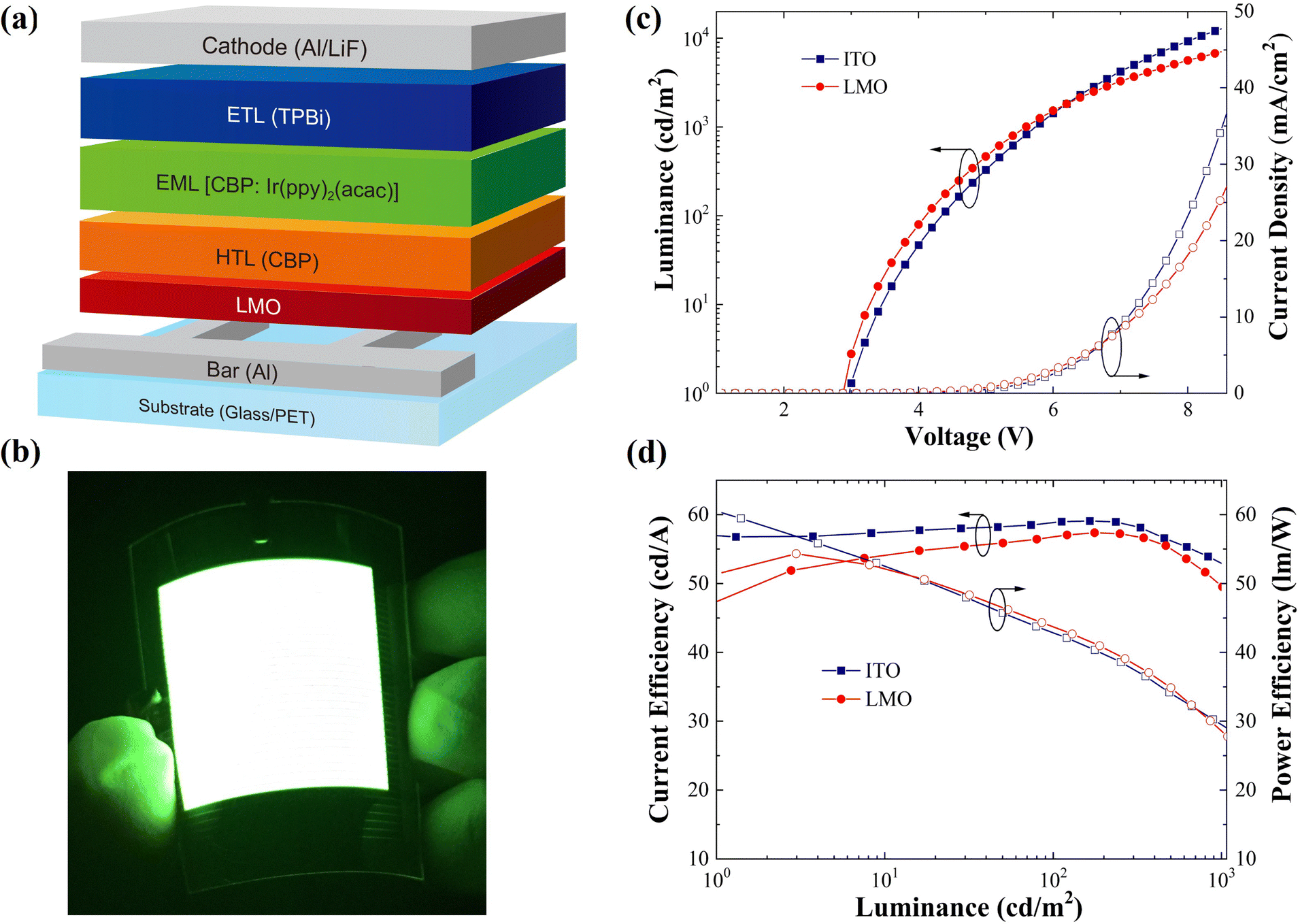 | ||
| Fig. 1 (a) Schematic OLED device structure. (b) A photographic picture of a flexible OLED (30 × 35 mm2) made with the LMO electrode on a plastic substrate. (c) Luminance–current density–voltage characteristics of OLEDs made with ITO and LMO electrodes. (d) Current efficiency vs. luminance and power efficiency vs. luminance characteristics of 2 × 12 mm2 active area OLEDs made with LMO and ITO electrodes. | ||
2.2. Physical properties
The optical transmittance and reflectance measurements were made using a Hitachi U-4100 UV-vis-NIR Spectrophotometer. The Fourier transform infrared (FTIR) spectra were obtained on a Thermo Scientific Nicolet iS10 infrared spectrometer with an attenuated total reflectance technique. The acquisition of all spectra was carried out by 16 scans per spectrum and in the range of 4000–600 cm−1 with a resolution of 4 cm−1. A background spectrum was recorded before collection of the spectrum of the new sample. The optical constants of the LMOs in the optical model were measured at the incident angles of 70° and 75° by an ELLIP-SR-I spectroscopic ellipsometer and Woollam RC2 ellipsometer. The 2 nm MoO3, 2 nm Al and MoO3 (2 nm)/Al (2 nm)/MoO3 (5 nm) (LMO) composite layer were thermally evaporated onto formvar stabilized with carbon support films, which were carried out by transmission electron microscopy (TEM). Transmission electron microscopy experiments were conducted using a Tecnai G2 TF30 S-Twin microscope operated at 300 kV, using monochromated Al Kα radiation (hν = 1486.7 eV) for XPS spectra and non-monochromated He Iα radiation (hν = 21.22 eV) for UPS spectra. XPS spectra were collected using a take-off angle of 75°. UPS spectra measurements were made at a take-off angle of 88°. During UPS measurement, the sample was held at a negative bias of −15 V relative to the spectrometer. The instrument is a PHI 5500 system.2.3. Charge transport
Variable temperature I–V measurements were performed by using a high and low temperature vacuum probe station (Cindbest CGO-4). The LMO was made with embedded finger electrodes to measure the lateral conductance.3. Results and discussion
Fig. 1(a) shows a schematic of the OLED device structure using the LMO electrode. The device structure consists of various functional layers stacked sequentially as: substrate/Al contact bar/LMO/CBP (20 nm)/CBP:Ir(ppy)2(acac) (8 wt%, 30 nm)/TPBi (65 nm)/LiF (1 nm)/Al (100 nm). The LMO is made by sequential deposition of 2 nm MoO3, 2 nm Al, and 5 nm MoO3. As will be discussed in the following text, spontaneous interfacial chemical reduction reactions lead to the formation of the Mo4+/Al3+/Mo4+/Mo6+ structure in the LMO. Details on optimizing the various MoO3/Al/MoO3 layer thicknesses are provided in Fig. S1 (ESI).† The thickness of TCO was critical in achieving the desired balance between optical transparency and electrical conductivity.Thinner films risk compromising conductivity, while thicker films reduce transparency.2 The LMO structure with a thickness of ∼10 nm optimizes the trade-off between optical transparency and electrical conductivity, achieving a performance superior to today's industrial staple material ITO. The LMO electrode's simple fabrication process, cost-effectiveness, superior optical and electrical properties, unique conduction mechanism and compatibility with flexible substrates position it as a promising solution for optoelectronic devices. To make electrical contact with the LMO, 100 nm-thick Al grid lines (0.1 mm wide and spaced 0.9 mm apart) are deposited, as schematically shown in Fig. 1(a). To illustrate the LMO's facile scale up potential, Fig. 1(b) shows a large area 30 × 35 mm2 flexible OLED made on a LMO-coated PET plastic substrate. For quantitative study of the LMO electrodes, we made relatively small area (2 × 12 mm2 active area) OLEDs. As shown in Fig. 1(c) and (d), the LMO-based OLEDs show excellent electrical characteristics, similar to those of regular ITO-based OLEDs.
Shown in Fig. 2(a) are LMO and ITO OLED emission spectra taken at various viewing angles. More detailed spectra at various viewing angles are provided in Fig. S2 (ESI†). Amazingly, the LMO-based OLED has emission spectra invariant of viewing angles. This is in stark contrast to typical OLEDs which show a relatively strong angular variation of the emission spectra. Theoretical optical calculations for various types of OLEDs at various viewing angles are provided in Fig. S2 (ESI†). The theoretical optical modeling analysis indicates that this unique optical output characteristic is related to LMO's excellent optical constants that match well with those of the OLED organic materials. The LMO's optical constants were measured using a spectroscopic ellipsometer and are provided in Fig. S3 (ESI†). As the optical characteristics of an OLED stack depend on the refraction index of the anode,45 the strong viewing angle dependence of the ITO device spectrum is related to an optical microcavity effect due to ITO's relatively high reflectance, as shown in Fig. 2(b). Fig. 2(b) shows the measured optical transmittance and reflectance spectra of the ITO-coated glass and the LMO (with Al grids)-coated glass. The LMO electrode structure exhibits excellent optical properties, the transmittance is higher and the reflectance is lower than that of the ITO film across the visible spectra. The transmittances of the ITO glass and the LMO electrode at 520 nm wavelength are 81.8% and 86.7%, respectively. It is noted that the opaque Al grids account for 9.2% of the total LMO electrode area.
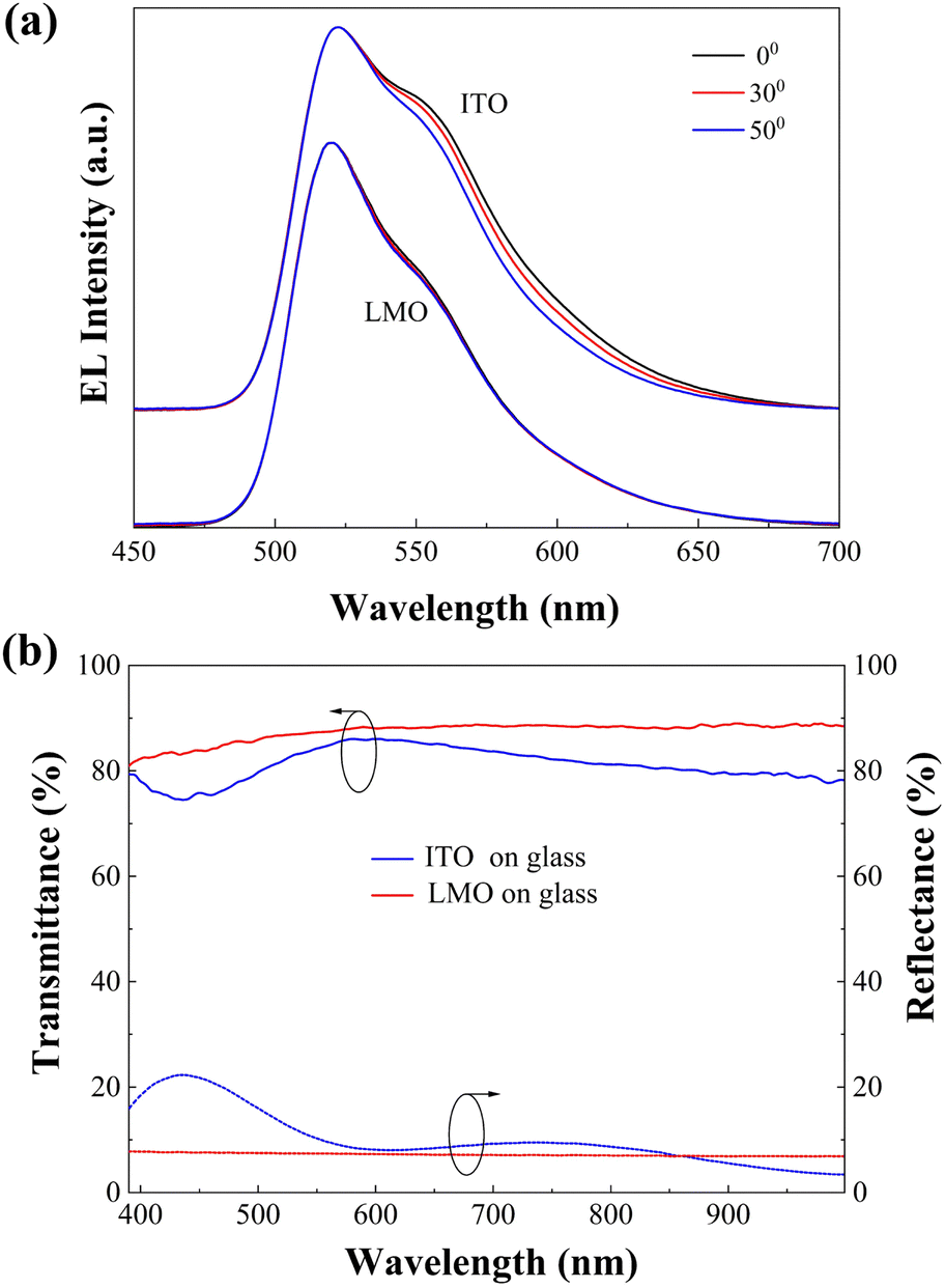 | ||
| Fig. 2 (a) Normalized emission spectra of LMO and ITO OLEDs at various viewing angles. (b) Optical transmittance and reflectance spectra of ITO-coated glass and LMO (with Al grid)-coated glass. | ||
To investigate the chemical structure of the LMOs, photoelectron spectroscopy (XPS/UPS) and FTIR spectra measurements have been conducted. Fig. 3(a) shows the Mo 3d and Al 2p core level spectra recorded from samples at various stages of deposition. Here heavily p-doped silicon substrate is used to prevent charging during XPS measurement. For Mo 3d, the d-shell spin–orbit splitting doublet peak, d5/2,3/2, is clearly resolved. For Al 2p, the p-shell spin–orbit split, p3/2,1/2, is not resolved due partially to the XPS's energy resolution. Fig. 3(a) shows that the first 2 nm MoO3 remains in 6+ oxidation states, as expected. Upon deposition of the 2 nm Al, this 2 nm Mo 6+ film converts to 4+. This spontaneous reduction reaction is somewhat expected, as the Gibbs free energy change for this reaction is −281.39 kcal mol−1 (for details see the ESI†). Fig. 3(a) also shows that this reduction reaction has converted metallic Al into alumina 3+. More detailed XPS tracking on the reaction is provided in the ESI† (Fig. S4 and S5). Molybdenum cation reduction at the interfaces also causes changes to the MoO3 valence band structure, as shown in the UPS spectra with various MoO3 thicknesses on Al substrate. Fig. S6 (ESI†) shows the valence regions near the Fermi levels for MoO3 films of various thicknesses on Al substrates. The above observations indicate that the interface reaction has converted the nominal Mo6+/Al0/Mo6+ into the Mo4+/Al3+/Mo4+/Mo6+ LMO structure.
 | ||
| Fig. 3 (a) Mo 3d and Al 2p core level XPS spectra recorded from samples at various stages of deposition. (b) Fourier transformed infrared spectra of LMO and MoO3 films. | ||
Fig. 3(b) shows the FTIR spectra of the LMO and 9 nm MoO3 thin films formed on glass substrates. The samples show absorption peaks in the wave number range of 4000–600 cm−1 corresponding to stretching and bending vibrations of metal–oxygen characteristic bonds. It is noteworthy that there are three absorption peaks in the FTIR spectra of LMO with the characteristic vibration bands at about 803 cm−1, 1030 cm−1 and 1182 cm−1. The peak of 1030 cm−1 corresponds to aluminum oxide films and the two other peaks belong to molybdenum oxide films. The small shoulder-shaped peak observed at 1182 cm−1 is assigned to the ending vibration of O atoms in Mo–O–Mo units and indicates the existence of Mo6+ in both LMO and MoO3 films.46–48 The medium intense peak of 803 cm−1 corresponds to the asymmetric stretching vibration of O–Mo–O short-length bonds in MoO2.49,50 The new most intense peak of 1030.81 cm−1 is associated to the Al–O bonds in Al2O3.51–53 The presence of these peaks provides clear evidence that the redox reaction does occur in the LMO structure. The FTIR results are in excellent agreement with the findings derived from the analysis of the XPS spectra.
The morphology and microstructure of the LMOs, the 2 nm MoO3 film, 2 nm Al film and the LMO film were studied by TEM. The high-resolution TEM images in Fig. 4 show that the LMO forms a featureless amorphous film.
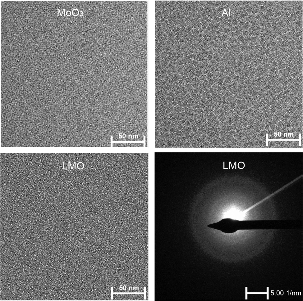 | ||
| Fig. 4 Transmission electron microscopy (TEM) micrographs of 2 nm MoO3, 2 nm Al and the LMO films. TEM diffraction of the LMO is also shown. | ||
Fig. 5 shows UPS spectra of the MoO3 thin films deposited on various substrates. New occupied electronic states are detected between the Fermi level (0 eV binding energy) and the valence band edge (∼2.5 eV). The formation of these gap states is related to the aforementioned interfacial redox-reaction. The expanded views of the gap state features for MoO3 films grown on Si and Al substrates are shown on the right panel of Fig. 5, which reveal two distinct gap-state features (d1 and d2). The lower binding energy feature, d1, occurs when only a small number of defect states exist, while the higher binding energy feature, d2, occurs when a large number of defect states exist in the band gap.54 The left panel displays the secondary electron cutoff used to derive the work function. For the MoO3 film on Si substrate, the d1 state, which is due to the oxygen vacancies, is always detected in MoO3, and has a work function of 6.36 eV. For the MoO3 film deposition on Al substrate, a strong charge transfer generates a significant amount of oxygen defect states at the interface, leading to clear UPS spectra of both d1 and d2. The work function of MoO3 deposition on Al substrate was determined as 6.00 eV. This UPS data corresponds well to the observation of a strong reduced oxide state Mo4+ in the XPS spectrum shown in Fig. 3(a) and the FTIR spectra shown in Fig. 3(b). These data suggest that the presence of gap states around the Fermi level may serve as conduction pathways for electron conduction in the LMO electrodes, as will be shown in the following text.
 | ||
| Fig. 5 The UPS spectra of the 2 nm MoO3 film grown on Si substrate and 3 nm MoO3 film grown on Al substrate. Gap states at various interfaces are labelled d1 and d2. | ||
To study the mechanism of charge transport in the LMO electrode, we have made a test device structure with embedded finger electrodes to measure the conductance with temperature variation. We have measured the I–V characteristics of the Glass/Al finger electrode (100 nm)/MoO3 (2 nm)/Al (2 nm)/MoO3 (5 nm)/protective coating (100 nm NPB) with temperature varied from 180 K to 360 K. To avoid disruptive changes caused by the protective coating layer, it is essential to control the sample's temperature below 375 K, due to the glass transition temperature of NPB being about 375 K.55,56 The measured I–V data show simple linear lines, like a classic Ohmic resistor with high conductivity (shown in Fig. S7, ESI†). The lateral electrical conductivity is calculated using:  . The temperature variable conductivity (black solid squares) is shown in Fig. 6(c), the experimental conductivity is fitted (red solid line) with the Mott variable range hopping conduction formula (Mott-VRH) and (blue solid line) the Efros–Shklovskii variable range hopping conduction formula (ES-VRH), respectively.
 | ||
| Fig. 6 (a) The UPS density of states spectrum relating the shallow valence band edge features. (b) A schematic of the localized gap states in LMO, illustrating their roles in hopping transport, the blue balls represent electrons, the blue dotted circle represents a hole, and the gray lines represent localized gap states around the Fermi level. (c) Electrical conductivity as a function of temperature in the LMO. The red line indicates theoretical data generated using the Mott variable range hopping conduction formula. The blue line was computed using the Efros–Shklovskii variable range hopping conduction formula. | ||
The variable range hopping (VRH) is a basic mechanism of charge transport in Anderson disordered systems with localized electronic states at low temperature. This VRH mechanism was initially proposed by Mott57 who assumed that the electronic states at the Fermi level are constant, and electrons can hop between localized states. Generally, electrons hop from site i to site j by the overlap of their localized wave functions, and the hopping from site i to site j is further assisted by thermal energy.58 Electron conduction will take optimized hopping paths. Thus, the probability P for hopping will be modulated with the phonon energy and is expressed as:
P = vph![[thin space (1/6-em)]](https://www.rsc.org/images/entities/char_2009.gif) exp(−|Ei − Ej|/kBT)exp(−2R/a) exp(−|Ei − Ej|/kBT)exp(−2R/a) | (1) |
 | (2) |
The Mott-VRH model occurs by phonon-assisted tunneling which is based upon the assumption that the density of states near the Fermi level is constant, and does not take into account electron–hole interactions. Considering the electron–hole Coulomb interaction, Efros and Shklovskii pointed out that a depletion of states near the Fermi level appeared.59 The electron hopping conduction has to overcome the Coulomb energy, and the derived conductance follows a T−1/2 law (ES-VRH). The temperature dependence of the electrical conductivity is based on:
 | (3) |
 | (4) |
For the ES-VRH model, the Coulomb energy plays an important role as hopping conduction requiring electrons to overcome Coulomb interaction energy. In principle, both Mott-VRH and ES-VRH laws for the same sample in different ranges of temperature can be observed.60 In some amorphous semiconductors, the transition from Mott's law to the ES-VRH law always occurs at very low temperatures.61,62
As illustrated in Fig. 6(c), we apply the ES-VRH and Mott-VRH charge transport models fitted to the experimental data. It was found that the Mott-VRH provides a slightly better fitting with the pre-factor σ0 = (2.29 ± 0.22) × 104 S m−1 and T0 = (1.23 ± 0.18) × 104 K. Fig. 6(a) shows the UPS density of states spectrum relating the shallow valence band edge features. The energy schematic of the localized gap states is shown in Fig. 6(b). These localized gap states around the Fermi level effectively introduce new conduction pathways for electron conduction in the LMO which shows Mott behavior. This Mott transport mechanism has been experimentally shown in other amorphous systems.63–65
As shown above, the presence of defect states around the Fermi level was detected directly by UPS in the LMO and they act like Anderson–Mott localized states, serving as a hopping conduction channel. This high electric conductivity explains LMO's capability of functioning as a metallic-like electrode for driving OLEDs.
4. Conclusions
Ultra-thin molybdenum oxide/aluminum oxide stacked LMO can be made by simple vapor-phase deposition, and can be used as a transparent conducting electrode in OLEDs. Through the photoelectron spectroscopy (XPS/UPS) and FTIR spectroscopy measurements, the existence of gap states near the Fermi level is detected directly in the LMO film. Variable temperature charge transport measurements of the LMO show that these gap states behave like Anderson–Mott localized states, which are found to form a conducting path in the LMO electrode. The LMO was investigated for use as a transparent anode to replace ITO in OLEDs. The transmittances of the ITO glass and the LMO electrode at the 520 nm wavelength are 81.8% and 86.7%, respectively. OLEDs with LMO electrodes have overall device characteristics better than those of OLEDs with ITO electrodes. Moreover, the LMO can be readily made on any type of substrate by simple physical-vapor deposition and thus this electrode technology has a high potential to be industrialized for fabricating future flexible OLEDs and other flexible optoelectronic devices.Author contributions
Tao Zhang conducted the experiments, analyzed the data, and drafted the manuscript. Peicheng Li, Nan Chen, and Dengke Wang contributed to the fabrication of films, photoemission measurements, and other characterizations. Nan Jiang provided expertise in optical modelling calculations. Jiale Su, Zhenxin Yang, and Changsheng Shi assisted with variable temperature current–voltage measurements. Qiang Zhu and Hongyu Yu participated in discussions of the results and provided feedback on the manuscript. Zheng-Hong Lu directed the research project and the manuscript organization. All authors have approved the final version of the manuscript.Data availability
The data that support the findings of this study are available from the corresponding author upon reasonable request.Conflicts of interest
There are no conflicts to declare.Acknowledgements
This work was supported by the International Joint Research Center for Optoelectronic and Energy Materials, the Key Laboratory of Yunnan Provincial Higher Education Institutions for Optoelectronics Device Engineering, and the National Natural Science Foundation of China (grant No. 62164012).References
- Y. Zhou, C. F. Hernandez, J. Shim, J. Meyer, A. J. Giordano, H. Li, P. Winget, T. Papadopoulos, H. Cheun, J. Kim, M. Fenoll, A. Dindar, W. Haske, E. Najafabadi, T. M. Khan, H. Sojoudi, S. Barlow, S. Graham, J. L. Brédas, S. R. Marder, A. Kahn and B. Kippelen, A Universal Method to Produce Low-Work Function Electrodes for Organic Electronics, Science, 2012, 336, 327 CAS.
- K. Ellmer, Past achievements and future challenges in the development of optically transparent electrodes, Nat. Photonics, 2012, 6, 809 CrossRef CAS.
- A. Sandstrom, H. F. Dam, F. C. Krebs and L. Edman, Ambient fabrication of flexible and large-area organic light-emitting devices using slot-die coating, Nat. Commun., 2012, 3, 1002 Search PubMed.
- D. Li, W. Y. Lai, Y. Z. Zhang and W. Huang, Printable transparent conductive films for flexible electronics, Adv. Mater., 2018, 30, 1704738 Search PubMed.
- S. Reineke, F. Lindner, G. Schwartz, N. Seidler, K. Walzer, B. Lüssem and K. Leo, White organic light-emitting diodes with fluorescent tube efficiency, Nature, 2009, 459, 234 CAS.
- Y. T. Lee, C. Y. Chan, N. Matsuno, S. Uemura, S. Oda, M. Kondo, R. W. Weerasinghe, Y. Hu, G. N. Iswara Lestanto, Y. Tsuchiya, Y. Li, T. Hatakeyama and C. Adachi, Bright, efficient, and stable pure-green hyperfluorescent organic light-emitting diodes by judicious molecular design, Nat. Commun., 2024, 15, 3174 CrossRef CAS PubMed.
- Y. L. Chang, Y. Song, Z. Wang, M. G. Helander, J. Qiu, L. Chai, Z. Liu, G. D. Scholes and Z. H. Lu, Highly Efficient Warm White Organic Light-Emitting Diodes by Triplet Exciton Conversion, Adv. Funct. Mater., 2013, 23, 705 CrossRef CAS.
- T. Huang, Q. Wang, H. Zhang, Y. Xin, Y. Zhang, X. Chen, D. Zhang and L. Duan, Delocalizing electron distribution in thermally activated delayed fluorophors for high-efficiency and long-lifetime blue electroluminescence, Nat. Mater., 2024, 23, 1523 CrossRef CAS PubMed.
- M. Du, Y. Feng, D. Zhu, T. Peng, Y. Liu, Y. Wang and M. R. Bryce, Novel Emitting System Based on a Multifunctional Bipolar Phosphor: An Effective Approach for Highly Efficient Warm-White Light-Emitting Devices with High Color-Rendering Index at High Luminance, Adv. Mater., 2016, 28, 5963 CrossRef CAS PubMed.
- T. Zhang, Y. Xiao, H. Wang, S. Kong, R. Huang, V. K. M. Au, T. Yu and W. Huang, Highly twisted thermally activated delayed fluorescence (TADF) molecules and their applications in organic light-emitting diodes (OLEDs), Angew. Chem., Int. Ed., 2023, 62, e202301896 CrossRef CAS PubMed.
- Y. Sun, N. C. Giebink, H. Kanno, B. Ma, M. E. Thompson and S. R. Forrest, Management of singlet and triplet excitons for efficient white organic light-emitting devices, Nature, 2006, 440, 908 CrossRef CAS PubMed.
- M. A. McCarthy, B. Liu, E. P. Donoghue, I. Kravchenko, D. Y. Kim, F. So and A. G. Rinzler, Low-Voltage, Low-Power, Organic Light-Emitting Transistors for Active Matrix Displays, Science, 2011, 332, 570 Search PubMed.
- K. Yang, D. Kwon, S. Nam, J. Kim, Y. S. Chung, H. Yoo, I. Park, Y. Park, J. W. Kim and J. Lee, Interfacial Exciton-Polaron Quenching in Organic Light-Emitting Diodes, Phys. Rev. X, 2024, 14, 041009 CAS.
- N. Sun, Q. Wang, Y. Zhao, Y. Chen, D. Yang, F. Zhao, J. Chen and D. Ma, High-performance hybrid white organic light-emitting devices without interlayer between fluorescent and phosphorescent emissive regions, Adv. Mater., 2014, 26, 1617 CrossRef CAS PubMed.
- G. Gonçalves, V. Grasso, P. Barquinha, L. Pereira, E. Elamurugu, M. Brignone, R. Martins, V. Lambertini and E. Fortunato, Role of Room Temperature Sputtered High Conductive and High Transparent Indium Zinc Oxide Film Contacts on the Performance of Orange, Green, and Blue Organic Light Emitting Diodes, Plasma Process. Polym., 2011, 8, 340 CrossRef.
- S. Parthiban, E. Elangovan, K. Ramamurthi, R. Martins and E. Fortunato, Investigations on high visible to near-infrared transparent and high mobility Mo doped In2O3 thin films prepared by spray pyrolysis technique, Sol. Energy Mater. Sol. Cells, 2010, 94, 406 CrossRef CAS.
- C. G. Granqvist, Transparent conductors as solar energy materials: A panoramic review, Sol. Energy Mater. Sol. Cells, 2014, 91, 1529 CrossRef.
- A. Lyubchyk, A. Vicente, B. Soule, P. U. Alves, T. Mateus, M. J. Mendes, H. Águas, E. Fortunato and R. Martins, Mapping the Electrical Properties of ZnO-Based Transparent Conductive Oxides Grown at Room Temperature and Improved by Controlled Postdeposition Annealing, Adv. Electron. Mater., 2016, 2, 1500287 CrossRef.
- E. Fortunato, P. Barquinha and R. Martin, Oxide Semiconductor Thin-Film Transistors: A Review of Recent Advances, Adv. Mater., 2012, 24, 2945 CrossRef CAS.
- S. M. George, Atomic Layer Deposition: An Overview, Chem. Rev., 2010, 110, 111 CrossRef CAS.
- M. G. Helander, Z. B. Wang, J. Qiu, M. T. Greiner, D. P. Puzzo, Z. W. Liu and Z. H. Lu, Chlorinated Indium Tin Oxide Electrodes with High Work Function for Organic Device Compatibility, Science, 2011, 332, 944 CrossRef CAS PubMed.
- R. N. Chauhan, N. Tiwari, R. S. Anand and J. Kumar, Development of Al-doped ZnO thin film as a transparent cathode and anode for application in transparent organic light-emitting diodes, RSC Adv., 2016, 6, 86770 RSC.
- R. Paetzold, K. Heuser, D. Henseler, S. Roeger, G. Wittmann and A. Winnacker, Performance of flexible polymeric light-emitting diodes under bending conditions, Appl. Phys. Lett., 2003, 82, 3342 CrossRef CAS.
- H. Wu, L. Hu, M. W. Rowell, D. Kong, J. J. Cha, J. R. McDonough, J. Zhu, Y. Yang, M. D. McGehee and Y. Cui, Electrospun metal nanofiber webs as high-performance transparent electrode, Nano Lett., 2010, 10, 4242 CrossRef CAS.
- L. Hu, J. Li, J. Liu, G. Gruner and T. Marks, Flexible organic light-emitting diodes with transparent carbon nanotube electrodes: problems and solutions, Nanotechnology, 2010, 21, 155202 CrossRef PubMed.
- R. V. Salvatierra, C. E. Cava, L. S. Roman and A. J. G. Zarbin, ITO-Free and Flexible Organic Photovoltaic Device Based on High Transparent and Conductive Polyaniline/Carbon Nanotube Thin Films, Adv. Funct. Mater., 2013, 23, 1490 CrossRef CAS.
- R. Jackson, B. Domercq, R. Jain, B. Kippelen and S. Graham, Stability of Doped Transparent Carbon Nanotube Electrodes, Adv. Funct. Mater., 2008, 18, 2548 CrossRef CAS.
- Y. M. Chien, F. Lefevre, I. Shih and R. Izquierdo, A solution processed top emission OLED with transparent carbon nanotube electrodes, Nanotechnology, 2010, 21, 134020 Search PubMed.
- D. Zhang, K. Ryu, X. Liu, E. Polikarpov, J. Ly, M. E. Tompson and C. Zhou, Transparent, Conductive, and Flexible Carbon Nanotube Films and Their Application in Organic Light-Emitting Diodes, Nano Lett., 2006, 6, 1880 CAS.
- Z. Wu, Z. Chen, X. Du, J. M. Logan, J. Sippel, M. Nikolou, K. Kamaras, J. R. Reynolds, D. B. Tanner, A. F. Hebard and A. G. Rinzl, Transparent, Conductive Carbon Nanotube Films, Science, 2004, 305, 1273 CAS.
- J. Wu, M. Agrawal, H. C. A. Becerril, Z. Bao, Z. Liu, Y. Chen and P. Peumans, Organic Light-Emitting Diodes on Solution-Processed Graphene Transparent Electrodes, ACS Nano, 2010, 4, 43 CrossRef CAS.
- F. Bonaccorso, Z. Sun, T. Hasan and A. C. Ferrari, Graphene photonics and optoelectronics, Nat. Photonics, 2010, 4, 611 CrossRef CAS.
- T. H. Han, Y. Lee, M. R. Choi, S. H. Woo, S. H. Bae, B. H. Hong, J. H. Ahn and T. W. Lee, Extremely efficient flexible organic light-emitting diodes with modified graphene anode, Nat. Photonics, 2012, 6, 105 CrossRef CAS.
- S. Pang, Y. Hernandez, X. Feng and K. Mullen, Graphene as transparent electrode material for organic electronics, Adv. Mater., 2011, 23, 2779 CrossRef CAS PubMed.
- Y. H. Kim, J. Lee, S. Hofmann, M. C. Gather, L. Müller-Meskamp and K. Leo, Achieving High Efficiency and Improved Stability in ITO-Free Transparent Organic Light-Emitting Diodes with Conductive Polymer Electrodes, Adv. Funct. Mater., 2013, 23, 3763 CrossRef CAS.
- Y. Li, X. Hu, S. Zhou, L. Yang, J. Yan, C. Sun and P. Chen, A facile process to produce highly conductive poly(3,4-ethylenedioxythiophene) films for ITO-free flexible OLED devices, J. Mater. Chem. C, 2014, 2, 916 RSC.
- S. De, P. E. Lyons, S. Sorel, E. M. Doherty, P. J. King, W. J. Blau, P. N. Nirmalraj, J. J. Boland, V. Scardaci, J. Joimel and J. N. Coleman, Transparent, flexible, and highly conductive thin films based on polymer-nanotube composites, ACS Nano, 2009, 3, 714 Search PubMed.
- P. C. Hsu, S. Wang, H. Wu, V. K. Narasimhan, D. Kong, H. R. Lee and Y. Cui, Performance enhancement of metal nanowire transparent conducting electrodes by mesoscale metal wires, Nat. Commun., 2013, 4, 2522 Search PubMed.
- B. Deng, P. C. Hsu, G. Chen, B. N. Chandrashekar, L. Liao, Z. Ayitimuda, J. Wu, Y. Guo, L. Lin, Y. Zhou, M. Aisijiang, Q. Xie, Y. Cui, Z. Liu and H. Peng, Roll-to-Roll Encapsulation of Metal Nanowires between Graphene and Plastic Substrate for High-Performance Flexible Transparent Electrodes, Nano Lett., 2015, 15, 4206 Search PubMed.
- J. Y. Lee, S. T. Connor, Y. Cui and P. Peumans, Solution-processed metal nanowire mesh transparent electrodes, Nano Lett., 2008, 8, 689 CrossRef CAS PubMed.
- A. R. Madaria, A. Kumar, F. N. Ishikawa and C. Zhou, Uniform, highly conductive, and patterned transparent films of a percolating silver nanowire network on rigid and flexible substrates using a dry transfer technique, Nano Res., 2010, 3, 564 CrossRef CAS.
- Z. Yu, Q. Zhang, L. Li, Q. Chen, X. Niu, J. Liu and Q. Pei, Highly flexible silver nanowire electrodes for shape-memory polymer light-emitting diodes, Adv. Mater., 2011, 23, 664 CrossRef CAS.
- T. Kim, A. Canlier, G. H. Kim, J. Choi, M. Park and S. M. Han, Electrostatic Spray Deposition of Highly Transparent Silver Nanowire Electrode on Flexible Substrate, ACS Appl. Mater. Interfaces, 2013, 5, 788 CrossRef CAS PubMed.
- L. Zhou, H. Y. Xiang, S. Shen, Y. Q. Li, J. D. Chen, H. J. Xie, I. A. Goldthorpe, L. S. Chen, S. T. Lee and J. X. Tang, High-performance flexible organic light-emitting diodes using embedded silver network transparent electrodes, ACS Nano, 2014, 8, 12796 CrossRef CAS PubMed.
- J. B. Kim, J. H. Lee, C. K. Moon, S. Y. Kim and J. J. Kim, Highly enhanced light extraction from surface plasmonic loss minimized organic light-emitting diodes, Adv. Mater., 2013, 25, 3571 CrossRef CAS PubMed.
- A. Hojabri, F. Hajakbari and A. E. Meibodi, Structural and optical properties of nanocrystalline α-MoO3 thin films prepared at different annealing temperatures, J. Theor. Appl. Phys., 2015, 9, 67 CrossRef.
- S. Uthanna, V. Nirupama and J. F. Pierson, Substrate temperature influenced structural, electrical and optical properties of dc magnetron sputtered MoO3 films, Appl. Surf. Sci., 2010, 256, 3133 CrossRef CAS.
- B. Gowtham, V. Ponnuswamy, G. Pradeesh, J. Chandrasekaran and D. Aradhana, MoO3 overview: hexagonal plate-like MoO3 nanoparticles prepared by precipitation method, J. Mater. Sci.: Mater. Electron., 2018, 29, 6835 CrossRef CAS.
- Q. Zhang, X. Li, Q. Ma, Q. Zhang, H. Bai, W. Yi, J. Liu, J. Han and G. Xi, A metallic molybdenum dioxide with high stability for surface enhanced Raman spectroscopy, Nat. Commun., 2017, 8, 14903 CrossRef PubMed.
- N. Dukstiene, D. Sinkeviciute and A. Guobiene, Morphological, structural and optical properties of MoO2 films electrodeposited on SnO2/glass plate, Cent. Eur. J. Chem., 2012, 10, 1106 CAS.
- M. Goudarzi, D. Ghanbari, M. Salavati-Niasari and A. Ahmadi, Synthesis and Characterization of Al(OH)3, Al2O3 Nanoparticles and Polymeric Nanocomposites, J. Cluster Sci., 2016, 27, 25 CrossRef CAS.
- A. Adamczyk and E. Długoń, The FTIR studies of gels and thin films of Al2O3-TiO2 and Al2O3-TiO2-SiO2 systems, Spectrochim. Acta, Part A, 2012, 89, 11 CrossRef CAS PubMed.
- W. Mozgawa, M. Król and T. Bajda, Application of IR spectra in the studies of heavy metal cations immobilization on natural sorbents, J. Mol. Struct., 2009, 924–926, 427 CrossRef CAS.
- M. T. Greiner, L. Chai, M. G. Helander, W. M. Tang and Z. H. Lu, Metal/Metal-Oxide Interfaces: How Metal Contacts Affect the Work Function and Band Structure of MoO3, Adv. Funct. Mater., 2013, 23, 215 CrossRef CAS.
- H. N. Yang, S. J. He, T. Zhang, J. X. Man, Y. Zhao, N. Jiang, D. K. Wang and Z. H. Lu, Molecular orientation and thermal stability of thin-film organic semiconductors, Org. Electron., 2021, 88, 106014 CrossRef CAS.
- José C. S. Costa, A. Mendes and Luís M. N. B. F. Santos, Thin film deposition of organic hole transporting materials: optical, thermodynamic and morphological properties of naphthyl-substituted benzidines, J. Mater. Sci., 2018, 53, 12974 CrossRef CAS.
- N. Mott, Electrons in glass, Nature, 1975, 257, 15 CrossRef CAS.
- W. F. Pasveer and M. A. J. Michels, Understanding Mott's law from scaling of variable-range-hopping currents and intrinsic current fluctuations, Phys. Rev. B: Condens. Matter Mater. Phys., 2006, 74, 195129 CrossRef.
- A. L. Efros and B. I. Shklovskii, Coulomb gap and low temperature conductivity of disordered systems, J. Phys. C: Solid State Phys., 1975, 8, L49 CrossRef CAS.
- D. Yu, C. Wang, B. L. Wehrenberg and P. Guyot-Sionnest, Variable range hopping conduction in semiconductor nanocrystal solids, Phys. Rev. Lett., 2004, 92, 216802 CrossRef PubMed.
- R. Rosenbaum, N. V. Lien, M. R. Graham and M. Witcomb, A useful Mott-Efros-Shklovskii resistivity crossover formulation for three-dimensional films, J. Phys.: Condens. Matter, 1997, 9, 6247 CrossRef CAS.
- H. Liu, A. Pourret and P. Guyot-Sionnest, Mott and efros-shklovskii variable range hopping in cdse quantum dots films, ACS Nano, 2010, 4, 5211 CrossRef CAS PubMed.
- H. R. Fallah, M. Ghasemi, A. Hassanzadeh and H. Steki, The effect of annealing on structural, electrical and optical properties of nanostructured ITO films prepared by e-beam evaporation, Mater. Res. Bull., 2007, 42, 487 CrossRef CAS.
- E. Prati, M. Hori, F. Guagliardo, G. Ferrari and T. Shinada, Anderson–Mott transition in arrays of a few dopant atoms in a silicon transistor, Nat. Nanotechnol., 2012, 7, 443 CrossRef CAS PubMed.
- N. Chen, J. X. Man, D. M. Zhang, D. K. Wang, J. T. Hu, C. S. Shi and Z. H. Lu, Yb2O3/MoO3 connecting electrodes for tandem organic semiconductor devices, Phys. Rev. Appl., 2024, 22, 054015 CrossRef CAS.
Footnote |
| † Electronic supplementary information (ESI) available: Details of the device performance, theoretical optical modeling calculations and a discussion on Gibbs free energy. See DOI: https://doi.org/10.1039/d4tc05338a |
| This journal is © The Royal Society of Chemistry 2025 |