
Advances in integrated quantum photonics for quantum sensing and communication
Taposhree
Dutta
 a,
Atefe
Safinezhad
b,
Mariia
Zhuldybina
b,
Ignacio Llamas
Garro
c,
Jesús Salvador
Velázquez-González
c,
Anuj K.
Sharma
d,
Bora
Ung
b and
Satyendra K.
Mishra
*e
a,
Atefe
Safinezhad
b,
Mariia
Zhuldybina
b,
Ignacio Llamas
Garro
c,
Jesús Salvador
Velázquez-González
c,
Anuj K.
Sharma
d,
Bora
Ung
b and
Satyendra K.
Mishra
*e
aDepartment of Chemistry, Indian Institute of Engineering Science and Technology, Shibpur, Howrah 711103, West Bengal, India
bDepartment of Electrical Engineering, École de technologie supérieure (ÉTS), 1100 Notre-Dame St W, Montreal, Quebec H3C 1K3, Canada
cNavigation and Positioning (N&P), Centre Tecnològic de Telecomunicacions de Catalunya (CTTC), Avinguda Carl Friedrich Gauss, 11 – PMT Building B6, 08860, Castelldefels, Barcelona, Spain
dDepartment of Applied Sciences National Institute of Technology, Delhi, India
eSpace and Resilient Communications and Systems (SRCOM), Centre Tecnològic de Telecomunicacions de Catalunya (CTTC), Avinguda Carl Friedrich Gauss, 7 – PMT Building B4, 08860 Castelldefels, Barcelona, Spain. E-mail: smishra@cttc.es
First published on 7th May 2025
Abstract
Integrated photonics has significantly transformed the field of quantum technologies throughout the past few years. A timely evaluation of the state-of-the-art and investigation of the different approaches pursued for integrated quantum photonics is highly appropriate in the context of the current second quantum revolution. With this perspective, we discuss the present issues and future developments related to various technological systems, relying on recent developments. Recent advances from a variety of subfields will be discussed, with emphasis on applications in quantum sensing and quantum communication. Significant advances in quantum communication and the quantum internet have been made in recent years in part due to the emergence of quantum photonic chips, whose low-cost, robustness scalability, and stability allow for new device possibilities with smaller footprints. Also discussed here are the achievements in quantum photonic chips with the most widely used photonic integrated fabrication platforms and the essential parts of integrated quantum communication systems. It highlights innovative concepts, advancements in the field, and cutting-edge developments, while addressing possible drawbacks and unresolved challenges.
Introduction
The Internet of Things (IoT) and communication technologies involve a wide range of sensors and microelectronics, currently being developed and incorporated incessantly into platforms that interact with the real world.1,2 In particular, optoelectronic devices and photonic systems have been extensively studied in a variety of constantly evolving human–machine interactive applications, including smart image sensors,3,4 displays,5 neuromorphic devices,6,7 biomedical healthcare systems,8,9etc. Previously, high-density and scalable optoelectronic integrated circuits and systems could be created with miniaturized, quick, and affordable photonics by using silicon-based complementary metal-oxide–semiconductor (CMOS) technology.10,11 Unfortunately, due to their restricted sensing and actuator qualities, conventional silicon-based optoelectronics are not able to fully meet the rising demand for more advanced and multifunctional state-of-the-art photonic devices. Furthermore, wearable and flexible applications cannot use silicon devices due to their hard and fragile nature.To overcome the shortcomings of the technologies in use today, a wide range of extremely sensitive and responsive photonic materials are being extensively investigated. Specifically, a number of nanoscale materials have been determined that satisfy the requirements of next-generation photonic technologies by demonstrating outstanding multifunctional and highly-sensitive characteristics (Fig. 1).12,13
 | ||
| Fig. 1 Outlook from 2D materials in quantum nano photonics. | ||
Extending nano photonics from nanometer scale to atomic scale is enabled by two-dimensional (2D) materials (Fig. 1). They are attributed with sustaining special optical excitations such as excitons in transition-metal dichalcogenides (TMDs)14 and plasmons in graphene,15–17 as well as their atomic thinness which naturally implied. Fundamental advancements in computing, security, sensing, and metrology are made possible by quantum mechanical phenomena, which use the laws of quantum physics to transmit information in a non-classical manner. Recently, from cutting-edge research and experimentation to commercial reality, this field has encompassed a wide range of technologies and applications. Quantum key distribution (QKD) is the most well-known example of this.18 The fundamental principle of QKD is to transfer secret keys between two distant entities by using the quantum states of photons. With the help of the quantum no-cloning theorem, the two communicating users can identify any attempt by an eavesdropper to obtain the key.19 Though its practical security has generated discussion in terms of the proof, research in QKD is paving the way towards a quantum internet where information security is ensured by the fundamental laws of physics, instead of complex mathematical problems.20 For instance, QKD studies using fiber-based and satellite-to-ground approaches have been proven at distances of 800 km in ultra-low-loss optical fiber21 and 2000 km in free space,22 respectively. More than 110 Mbit per s is now the maximum secure key rate that can be achieved over a single channel.23 Additionally, a great deal of research has been carried out on the security of everyday life QKD systems in order to overcome the current technological constraints.20,24 To accomplish both long-term key security and short-term authentication security, post-quantum cryptography has been integrated with QKD.25 Quantum teleportation has attracted a lot of attention despite QKD because it leverages quantum entanglement to transmit sensitive quantum information in a way which nearly impossible to reverse.26 Consequently, different quantum devices can be connected via quantum networks, providing previously unreachable capabilities that are demonstrably impossible with only classical information technology.27 Another significant area of quantum communication, known as quantum secure direct communication (QSDC) techniques,28 also made it possible to communicate data securely via a quantum channel. With the rapid evolution of this approach in recent years, individuals can now immediately send confidential information over secure quantum channels without exchanging encryption keys. Current technology can be used to build a QSDC network with end-to-end (E2E) security while paired with post-quantum cryptography.29 In recent years, nitrogen-vacancy (NV) centers in diamond have gained considerable attention as highly promising candidates for various quantum technologies.30 NV centers exhibit exceptional quantum coherence properties, even at room temperature, making them ideal for a range of applications, including communication, sensing, and information processing.31 Discrete optical devices such as single-photon sources and photodetectors, are usually used in the construction of conventional quantum communication systems, which enable fundamental improvement to security, computing, sensing, and metrology. These devices are often built independently using optical crystals (such as calcite – CaCO3, beta barium borate – BaB2O4, and lithium niobate – LiNbO3) and glasses (such as fused quartz and silica – SiO2), and coupled by free space or optical fibers. Though it is not very simple to optimize individual components to meet the exacting specifications needed for quantum information applications, such as ultra-low-loss, high efficiency, fast speed, and high fidelity, packaging and interconnects have always presented significant reliability and cost issues for conventional discrete optical designs, especially while interacting with large-scale networks that connect hundreds of thousands of users. For example, in order to reduce space and phase misalignment over time caused by environmental stressors and temperature fluctuations, strong mechanical and thermal stabilities are required. However, achieving these stabilities through global stabilization is challenging in a complex discrete optical system.
Apart from being smaller in size, quantum integrated devices offer two notable benefits over discrete optical systems: stability and scalability.32 By printing the chips as a single unit through lithography used in well-established batch semiconductor fabrication processes instead of building each component separately, scalability and mass production become feasible.33–35 Due to the circuit capacity to control deviations due to temperature changes or vibrations, stability is accomplished on a strong and lightweight solid-state substrate. For quantum information processing and extremely effective quantum communication, performance and integration levels must be attained, and these two aspects are essential. Integrated photonic chips have the potential to integrate various desirable attributes, including efficiency, affordability, scalability, flexibility, and performance, which are necessary for quantum communication applications. In this review, we discuss recent developments in quantum communication and the implementation of quantum-based sensing devices. We also review the materials used to design photonic devices. Integrated photonic materials, adaptable active and passive components for quantum state manipulation, and integrated single-photon and homodyne sensors are the main components of the chip-based quantum communication systems that we analyze. Then, we explore the development of on-chip devices for useful quantum communication applications like QKD and information-based techniques for example quantum mobility and entanglement distribution throughout. Lastly, we discuss the challenges and future prospects of photonic based quantum sensors.
1. Quantum sensing
Light-based sensors can also be improved through the help of quantum optics.36,37 The precision of sensors that rely on classical light is restricted by the signal-to-noise ratio (SNR) of the measurements. It is commonly referred to as the shot noise limit of photodetection, where the precision is limited at a fixed intensity of light impinging on the sensor due to the “graininess” of photoelectron counts. A two-path interferometer arm for the measurement of the refractive index changes can be linked to phase shifts measured by the classic optical sensor. Variations in temperature, pressure, presence of contaminating molecules, or other noteworthy characteristics are all related to changes in the refractive index. Under such configuration, the precision Δϕ with which an optical phase shift ϕ might be measured with classical light is set by shot noise. The precision scales as N−1/2, where N is the average number of utilized photons. Sensors based on quantum effects outperform the classical ones as they offer high precision and ability to operate at the nanoscale level.38 Coherence and entanglement are examples of quantum phenomena that can be used to increase measurement sensitivity, which in turn can increase parameter estimation precision and the spatial and temporal resolution of imaging systems. They can also be used to compensate classical impairments found in the channel such as chromatic dispersion. The most well-known system involves the arrangement of N photons in a superposition in one path. These states, designated as “N00N” states, offer an improvement in precision to the point where Δϕ scales as N−1, also called the Heisenberg limit.39–42 It has not yet been feasible to demonstrate a true improvement in precision after taking into account all of the photons that are placed into the interferometer but do not pass through or are not detected since such entangled states are extremely sensitive to losses. Thus, recent work has concentrated on how to strengthen the software against noise and flaws that arise in practical scenarios.43–46 Although it is not always easy to generate the necessary states and uncover which types of quantum states are useful—generally those that have some entanglement, but not the maximum achievable for a specific number of photons.47,48 Furthermore, in the presence of flaws, it is impossible to reach the Heisenberg limit; yet, for some types of noise, it is conceivable to advance beyond the conventional quantum limits, and in a broader sense, to obtain an important advancement in precision for a given amount of light.49–51 It has been shown that gravitational wave sensors built on optical interferometers have increased precision. In order to create a “squeezed state” in the optical oscillation, light with extremely low noise in its field amplitude at specific points is injected into the interferometer's “empty” or vacuum input port. One port is used to inject high-power laser light into another. This technique improves the likelihood of detecting gravity waves by replacing the absence of light at the vacuum port with compressed light, which raises the SNR of the measurements by 2.0 dB.52Nowadays sensors that estimate key parameters beyond the classical strategies are being focused on. These can be used, for instance, in situations where the parameter to be evaluated contains random noise.38,53 As an example, random phase changes may result from ambient fluctuations or temporal variations in the sample itself in an interferometer when the phase shift due to a material sample is to be determined. Consequently, the phase shift's variance and mean are unknown values. The boundaries of the precision that quantum physics permits in this instance exhibit certain noteworthy characteristics. Specifically, it is more effective to estimate several parameters jointly rather than individually.54 Furthermore, imaging can be viewed as an estimation problem with multiple parameters.55 The phase shift at each pixel in a picture can be estimated in phase contrast microscopy. The collective estimation of a set of phase shifts is also more efficient than individual estimation of each shift.56 However, achieving the necessary quantum states for enhanced accuracy is not easy. In addition, one of the research studies emphasizes evaluating the closest one may proceed to the quantum improved accuracy with quantum light that can be produced in a controlled environment.57,58 Among the quantum systems under investigation, NV centers in diamond stand out due to their unique sensitivity to strain, magnetic and electric fields.59 NV centers can be utilized in quantum magnetometry with high spatial resolution, enabling the measurement of minute variations in magnetic fields.60 This capability makes them particularly useful in applications such as nanoscale magnetic resonance imaging and biological sensing.61 Their spin properties allow for the detection of extremely subtle changes, enabling precise, real-time analysis at the nanoscale.62 In addition to their remarkable sensitivity, NV centers can operate effectively at room temperature, without requiring the complex, bulky and expensive cooling systems often necessary for other types of quantum sensors. The latter characteristic broadens their applicability across a variety of fields, allowing them to be easily integrated into systems where maintaining low temperatures is not feasible.38 Moreover, their non-invasive nature permits the measurement of key parameters without disrupting the system under observation, a critical feature for sensitive environments such as biological systems or nanomaterials.63
Using these methods with distributed sensors is a key application; it is possible to combine safe monitoring of remote sensors with improved multi-sensor scanning accuracy. These improvements might prove beneficial for various fields including light-based gravimetry, magnetometry, acceleration measurements, duration and frequency requirements, and imaging technologies like microscopy.64
2. Fundamental advances for quantum photonic devices
The road towards more compact quantum communication systems with higher efficiency and complexity has been leveled and smoothed through photonic micro-nano-integration. The three facets of integrated quantum communication are summarized as follows: (i) photonic materials for integration;65–67 (ii) quantum photonic elements like high rate modulators,68,69 quantum optical sources,70 and extremely effective photodetectors71 and (iii) their uses in QKD and quantum teleportation (Fig. 2).72 Essential photonic components in chip-level configurations must be redesigned and optimized for specific quantum information applications because the materials, preparation techniques, and structural designs used in photonic integration differ significantly from those used in discrete systems. An explanation of the pertinent technical research is provided, including quantum radiation sources, integrated photonic system packaging methods, quantum detectors, encoding and decoding modules. Using periodically poled lithium niobate waveguides and silica-on-silicon planar light-wave circuits (PLCs) for interferometers, the integration of photon sources is considered one of the earliest initiatives in this field.73,74 These integrated devices had excellent efficiency and temperature-stabilized performance proving their inherent suitability over their separate and bulky discrete components. Later on, a great deal of additional materials was investigated, and significant advancements were made in the creation, modification, and detection of quantum states of light on-chip for applications including quantum communication and other forms of quantum information. The most widely used materials systems for chip-based quantum communication implementations are silicon-on-insulator (SOI), silicon nitride (Si3N4), lithium niobate (LiNbO3), gallium arsenide (GaAs), indium phosphide (InP), and silicon oxynitride (SiOxNy).32,75 Strong optical nonlinearity for nonclassical state generation, a high refractive-index contrast for high-density integration, and excellent compatibility with advanced complementary metal-oxide–semiconductor (CMOS) processes—which have been widely used in the semiconductor industry is provided by SOI. Nevertheless, it is difficult to completely integrate all of the necessary parts of a quantum communication system due to the lack of lasing capabilities.76,77 Monolithic system integration is possible with III–V semiconductor platforms (GaAs, InP, etc.), but the cost is higher and the integration level is lower. It is evident from the unavoidable flaws in every material and its production method that no other platform can offer every feature needed for quantum communication applications. Hybrid integration, which combines the benefits of several systems, is an achievable solution.75 Initiatives such as integrated superconducting nanowire single-photon detectors (SNSPDs) and integrated lasers for weak coherent pulse production have been undertaken in an endeavor to realize heterogeneous quantum photonic systems.71,78 | ||
| Fig. 2 An overview of quantum communication based on quantum photonic chips. | ||
These days hybrid integration with 2D materials like graphene, black phosphorous (BP), transition metal dichalcogenides (TMDs) among others, is receiving attention due to their unique properties.79–81 In them, atomic planes are stacked one layer on top of the other in a predetermined order, commonly known as “van der Waals (VdWs)” heterostructures.82 The dangling-bond-free surfaces of atomic sheets offer significant flexibility in enabling the construction of arbitrary VdWs heterostructures, in contrast to conventional heteroepitaxy. Though it can also be used to integrate mixed-dimension materials, such as 2D materials with 0-dimensional quantum dots (QDs), 1-dimensional nanowires, or 3-dimensional bulk materials, this property enables the integration of extremely dissimilar 2D materials.83 In addition to these hybrid systems, nitrogen-vacancy (NV) centers in diamond have emerged as promising platforms for advancing quantum photonic systems. NV centers exhibit good coherence times and stable single-photon emissions, which are critical for quantum communication applications, such as quantum key distribution (QKD), secure quantum networks and quantum sensing.84 Their ability to operate in both cryogenic and ambient conditions enhances their reliability in various quantum systems.85 NV centers have been successfully embedded in chip-scale photonic platforms, including waveguides and resonators, which allow for precise manipulation and detection of quantum states, making them ideal for scalable, high-performance quantum communication technologies.86 Several significant technologies have emerged as alternatives for on-chip quantum communication implementation, such as semiconductor quantum dots (QDs) interfaced with photonic nanostructures, coherent pulse generation, and diamond-on-insulator.78,87
3. Techniques for integrated photonics
Today, a number of photonic integration materials like LiNbO3 (often abbreviated “LN”), silica (SiO2), semiconductor and highly advanced 2D materials are used to assemble the essential building blocks that enable the production and manipulation of quantum states of light on a single chip (Fig. 3).88,89 We explain them here following significant requirements for ideal quantum integrated photonic systems.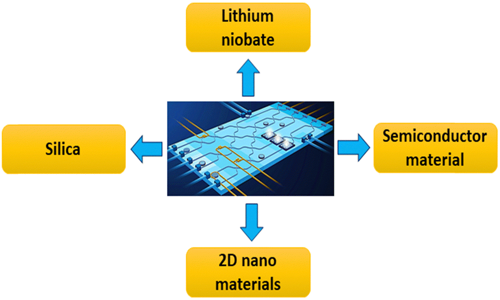 | ||
| Fig. 3 Advanced photonic materials used in the fabrication of quantum states of light on a single chip. | ||
3.1. Emission of quantum light
This property is directly related to photon entanglement and includes the generation of discrete photon-pairs, vacuum-squeezed states of light, and hybrid states that rely on different distinct and continuous quantum components.90,91 It can be based on three-wave, four-wave mixing, or biexciton de-excitation.3.2. Development of a single photon
This feature provides the ability to integrate probabilistic single-photon emitters based on the photon-pair creation, in contrast to consistent genuine single-photon emitters.92–963.3. Nonlinear and linear on-chip components
Filters, beam splitters, and multiplexers are examples of devices which offer the capacity to passively direct and shape light in both the spatial and frequency domains. Electro-optic modulation is another tool which is used for actively modifying the quantum elements of light.97–1003.4. Adaptability
It was associated with the potential of a higher integration capability. It comprises the effective sizes of the different components that allow for the estimation of the integration scaling factor, material propagation losses, and refractive index steps in waveguides.101,1023.5. Quantum light detectors
Quantum states of light require on-chip detectors with high jitter, low noise, and high efficiency for certain applications. These detectors could be high-performance intensity photodiodes for measuring brilliant nonclassical states of light or single-photon detectors.103,104 Photodiodes are made from semiconductor materials that are doped with p-type and n-type elements, which determines the observable optical wavelengths based on the appropriate material's bandgap. A charge carrier depletion area with a corresponding internal field forms at the p–n junction. A mobile electron is excited and creates an electron–hole pair when light with enough photon energy strikes the diode. A detectable photocurrent proportional to the quantity of incident photons is produced by an internal field over the depletion area. Photodiode performance is influenced by its noise behavior, which is determined by the dark current, noise-equivalent power, and responsivity. The ratio of incident photons to detected photons, or generated electron–hole pairs, is known as the quantum efficiency (η). The quantum efficiency varies according to the wavelengths and semiconductor materials employed, but it can achieve extremely high values exceeding 95%. Conventional photodiodes lack single-photon sensitivity, which means they cannot detect single photons or light with low photon numbers due to noise contributions from thermal excitations. These noise contributions can be mostly disregarded in bright light, while for an ideal detector with η = 1 the light statistics and photon current are related as
Here, ne is the number of photoelectrons; e is the elementary charge. An ideal detector preceded by a beam splitter, which represents an effective loss of 1–η, can be used to imitate the real detector. Whereas, single photon detection requires internal amplification of the absorbed photon's signal to generate an electrical output that surpasses the noise level. Avalanche photodiodes (APDs) can achieve this because of their unique architecture, which includes a multiplication zone in addition to an absorption region. In the avalanche process, secondary electrons are produced by high voltage across the multiplication zone if photon absorption produces an electron–hole pair. Therefore, an avalanche process with an exponential development of free carriers that results in macroscopic photocurrents can be initiated by a single electron–hole pair. Lowering the applied voltage is necessary to quench the avalanche, preventing damage and allowing for subsequent detection. The current flow is actively stopped in active quenching circuits to speed up the APD's reset. The quantum efficiency in the context of APDs represents the probability that a single photon will be captured. At wavelengths between 700 and 800 nm, an APD's quantum efficiency typically reaches a maximum value of 60% to 70%; at wavelengths between 1200 and 1700 nm, the most recent generation of APDs achieves efficiencies exceeding 25%. The dark count rate, which indicates the number of detection events that occur in the absence of an optical signal, is a measure of the detector's noise level. For APDs at 800 nm, dark count rates as low as 100 counts per second can be readily attained. The APDs’ dead time indicates the bare minimal amount of time required to record a series of detection events. Active gating requires dead times of more than 1 μs for APDs operating at telecom wavelengths, while dead times as short as 50 ns are typical for 800 nm APDs.105
3.6. Interaction with CMOS
CMOS exhibits the ability to construct electrically driven devices as well as the possibility of integration with electronic component layers.106,107 The standard CMOS manufacturing process is suitable for several kinds of microsystem class development, including temperature, optical, and magnetic sensors, which have been commercially available for some time.108 The combination of CMOS technology with the electrodeposition of metal coils and ferromagnetic cores has resulted in the development of new magnetic sensing devices, including fluxgate sensors and inductive proximity sensors.109,110 Moreover, CMOS technology in conjunction with appropriate micromachining and thin-film deposition techniques has led to the production of an increasing number of microelectromechanical systems (MEMS). The extra fabrication stages might be carried out in between the standard CMOS processes (intermediate-CMOS), before (pre-CMOS), or after (post-CMOS).111–1143.7. Integration with memory
Memories in the context of quantum communication can be built as either emissive systems, which emit a photonic qubit on demand whose state is entangled with an internal degree of freedom of the memory, or as “in–out” systems, which absorb and store an incoming qubit. In the latter case, one “stores” the quantum states by using quantum state teleportation. Every type of memory has its own unique qualities and is used in various protocols.1154. Integrated photonic materials
Here, we discuss the currently developed integrated photonic materials.4.1. Lithium niobate (LN)
In the past, one of the key technologies for quantum integrated photonics has been crystalline lithium niobate (LN).116,117 Large second-order nonlinear coefficients (both opto-optic and electro-optic) and low optical transmission losses are among the well-known optical characteristics of LN waveguides, which make them an ideal choice for the creation of effective integrated photonic devices for both classical and quantum information applications.118 Quantum states can be created in LN with unmatched brightness using spontaneous parametric down-conversion (χ(2) based), which is simpler to pump rejection than spontaneous four-wave mixing in Si (χ(3) based).119 These states can then be further customized and manipulated through domain engineering. Monolithic LN chip development has been slowed down in favor of LN-on-Insulator (LNOI) as it offers a smaller footprint compared to the cm-scale typical footprint of traditional (i.e., proton-exchanged waveguide) LN circuits. With the potential to achieve Si and SiN chip sizes, this technology is currently opening the door to the realization of novel quantum photonic devices with unprecedented heights of performance and scalability.120 For example, the bandwidth of electro-optic modulation has been increased to over 100 GHz, and though the fabrication process is not as advanced, the scaling factor is still equivalent to Si photonics.97,121 The ability to create electro-optically reconfigurable circuits that can function well at cryogenic temperatures is another crucial aspect of LNOI. Niobium titanium nitride stripes patterned on top of the waveguides have been used to demonstrate their integration with superconducting nanowire single-photon detectors (SNSPDs).122,123 Due to the usage of rare earth ion-doped crystal, LN waveguides are eventually, even at this early stage of research, compatible with quantum memory.1244.2. Silicon (Si) and silicon carbide (SiC)
Si photonics is a relatively new platform that has made a big splash in the quantum world. It is fully compatible with CMOS technologies and permits the production and manipulation of near-infrared light quantum states on-chip.125–127 In terms of technical aspects, Si quantum photonics gained attention due to its advanced integration density factor, effective third-order optical nonlinearities, and the precise design and processing workflow. The diameters of the passive and active components are usually about 100 μm in size. Even though it lacks a natural electro-optical coefficient, which causes weak optical modulation through local heating, it can still be used for a number of additional features, including wavelength and photon-routing.128 At the moment, the primary impediment to the platform's scalability is the relatively high propagation losses (≤0.1 dB cm−1) and two-photon absorption in Si waveguides (Fig. 4) | ||
| Fig. 4 (a) Si ring resonator integration on a 45 nm CMOS SOI chip,129 Copyright (2015), Optica publishing group; (b) analysis and development of a two-photon entangled state on-chip. Beyond the SOI chip are detectors and a pump laser,130 Copyright (2015) Springer Nature; (c) with silica waveguides, a fully reconfigurable circuit that can execute each linear optical operation feasible for its size could be created,131 Copyright (2015), Science. | ||
In order to offset a lower third-order nonlinearity, the use of SiN is now addressing this issue by minimizing two photon absorption, extending the transparency range to the visible, and reducing propagation losses down to ≤0.1 dB cm−1. Nitrogen vacancy (N-V) centers in Si and SiC are the most researched solid-state emitters in terms of single-photon emission, mostly due to progressively improved nanofabrication processes.132–134 Due to wavelength incompatibilities with telecom fibers and recent significant advancements in nuclear magnetic resonance (NMR) spectroscopy,135 the platform in the particular case of SiC has been primarily focused on quantum computation, simulation, and quantum rebroadcast techniques.136,137 Furthermore, SiC has been studied as a platform for integrating nanodiamonds to create scalable hybrid photonic devices. However, one aspect that has prevented the SiC material from being used structurally is its low fracture toughness. In order to overcome this problem, nano powders have been found to improve mechanical and sinterability qualities due to their larger surface areas and specific surface activities compared to micron-sized powders.138 Reinforcing phases (such as aluminium, boron, or yttrium-based oxide) are primarily utilized for consolidation in order to achieve fine-grain size and high densification for SiC. The mechanical properties of the composite are frequently improved by the introduction of these reinforcing components.139 However, because the oxide phase at the grain boundary can impair the mechanical behaviour at high temperatures, they pose some difficulties when exposed to radiation (neutron swelling or absorption). Because the resulting composites yield a material with improved mechanical properties, the breakthrough in ceramic matrix composites has attracted a lot of interest in overcoming the difficulties of ceramics. As a result, the final products have been highly valued in airframes, aircraft engines, space structures, and other fields where creep and alternating load are common. A useful method for the upcoming development of high-temperature, aerospace, and other lightweight systems is demonstrated by a variety of functional structures that use ceramic matrix composites and coatings. These could be employed in applications that need to operate over a wide range of temperatures and pressures, which could be a problem for future cutting tools and hypersonic materials.
Nanodiamonds containing NV centers are deposited on SiC micro disks, which support high-quality factor whispering gallery modes (WGMs).140 SiC-based platforms enable light to propagate through both SiC and diamond, increasing light–matter interaction compared to other hybrid platforms.141 Finally, the interaction of light and sound waves at the quantum level, either in opto-mechanics (usually, kHz–MHz range) or through stimulated Brillouin scattering (SBS) (usually, in the 10 GHz range), is a significant area of research for Si-based components.142,143
4.3. III–V and III–N semiconductors
A direct band gap and well-developed growth and processing methods have historically allowed semiconductor materials to demonstrate quantum dot (QD) structures for the deterministic generation of single photons.144–146 Later, deterministic entanglement generation was achieved through the use of the biexciton cascade.147 It is possible to obtain GHz high-purity single photon emission and significantly boost the spontaneous emission rate of QDs by coupling them spectrally and spatially to microcavity modes.148 Novel experiments tie single-photon sources to photonic circuits to execute optical quantum computing tasks, going beyond the usage of a photonic structure to optimize the extraction of single photons to an optical fiber.149 GaP, with its high refractive index and strong second-order nonlinearity, is integrated with NV centers in nanodiamonds, allowing efficient coupling of optical fields to these quantum emitters, improving photon emission efficiency.150,151 Furthermore, GaAs and associated chemicals offer a future pathway. They show enormous integration potential since this platform combines a high second-order optical susceptibility that makes it possible to integrate SNSPDs with entangled photon sources based on nonlinear optical processes (Fig. 5). | ||
| Fig. 5 (a) Integrated GaAs wave guides serve for achieving both passive and active photonic elements,152 Copyright (2014), Elsevier; (b) a ridge waveguide structure with a Nb-NSSPD and a layer of GaAs/InGaAs QDs. The waveguide gathers and detects the fluorescence from a QD on the semiconductor. Insets display the AFM image of a QD, the SEM image of the SNSPD, and the calculated waveguide mode profile,153 Copyright (2015), American Chemical Society. | ||
Moreover, they provide a direct on-chip integration of an active laser domain, opening the door for electrically powered devices.154,155 In a similar vein, GaN is the second most used semiconductor in the world after Si, and it is possible to fully use the knowledge of technology that has been established so far for high-power, high-frequency, and solid-state illumination. There are existing electrical injection and photonic building blocks (air/GaN distributed Bragg reflectors, optical waveguides, in and out couplers, photonic crystals, etc.) for the GaN platform. New material aluminum nitride (AlN) is appropriate for photonic integrated circuits that can be made larger. In addition to showing tremendous promise for the realization of on-chip photon-pair sources based on spontaneous parametric down-conversion (SPDC), its significant intrinsic second-order nonlinearity (χ(2)) also allows for integrated low-loss and high-speed electrooptic phase modulators.156 Dense integration and a tiny device footprint are made possible by the strong refractive index contrast between silica-cladding layers and AlN waveguides.
4.4. Silica
Silica provides a very strong and diverse waveguide technology, but it also lacks an electro-optic coefficient and has a weak third-order nonlinear coefficient. Femtosecond laser direct-writing (FLDW) has garnered attention as a method for creating intricate linear waveguide circuits because it has the lowest intrinsic propagation loss of any material in the infrared (IR) regions. It has intrinsic three-dimensional (3D) routing capabilities and enables high-speed device production without the requirement for lithographic masks. Rapid small-scale circuit prototyping has been used in quantum photonics to enable research on single- and entangled-photon production, boson sampling, and hitherto impractical quantum entanglement.157,158 For instance, silica waveguides and resonators play a crucial role in single-photon generation circuits. When coupled with color centers in nanodiamonds, they enhance light–matter interaction through whispering gallery modes (WGMs), significantly boosting photon emission efficiency.159,160 Quantum integrated photonics has demonstrated significant promise using a more traditional method, which goes beyond a laser-written waveguide. The first quantum gate was shown in 2008 using a planar waveguide made of silica on a Si wafer.161 Since then, advances in reconfigurable circuits combining up to 15 interferometers have been demonstrated.1314.5. 2D materials
Two-dimensional (2D) materials offer a way to push nano photonics into the atomic scale, beyond the nanometer scale. Their atomic thinness is a natural cause of this, but they also support special optical excitations, including graphene plasmons (GP),15 excitons in transition-metal dichalcogenides (TMDs),14 nanoparticle-on-metal (NPoM) systems,162 hexagonal boron nitride (hBN)163etc. Due to their distinct optical sensitivity, 2D materials allowed light–matter interaction to be stretched to the atomic limit. For instance, the realization of perfect absorbers and highly reflective mirrors that are only one monolayer thick was made possible by the quantum response of excitons in monolayer semiconductor TMDs.164,165 Furthermore, these materials’ excitonic properties were relatively easy to control, which made it possible to manipulate their radiative lifetime through optical cavities and achieve quantum nonlinear effects at the single-photon level. These developments could pave the way for the development of new platforms based on strongly correlated photons.164,166,167 Similar to this, single-plasmon response and quantum effects arise from graphene plasmons (GPs) supported by finitized-sized graphene structures.168,169 Whereas, a nanoparticle-on-metal (NPoM) system, which is made up of a metal particle with a nanometric size (often a cube or a sphere) separated from a metallic surface by an extremely thin dielectric spacer is one example of a system for light confinement (Fig. 6(a)).162 The nanoparticle and metal surface can form a gap surface-plasmon mode with a tiny mode volume, large field enhancement (104), and Purcell factor (105–107) due to the presence of NPoM.170 Thus, it has made possible the response of nano antennas, spontaneous emission sources, and strong coupling at room temperature.171–173 Quantum nonlocal effects play a significant role in reducing the potential field enhancement, but the NPoM system extinction also causes greater damage because of its plasmonic nature.174,175 In terms of technology, these enable the construction of NPoM systems with atomic precision layer after layer, reducing the dielectric spacer to a single monolayer (Fig. 6(b)).176,177 | ||
| Fig. 6 Techniques for confining optical modes in nanophotonic cavities. (a) The nano cube-on-metal (NCoM) device interacts with an optical emitter while supporting a gap SPP in the VIS/NIR that is confined between a metal nano cube and a metal surface. (b) A vibrational molecular resonance interacts with the graphene-plasmon-magnetic resonator (GPMR) system, which supports a GPs in the MIR/THz confined between a metal nano cube and a graphene sheet. (c) The GPMR system exhibits values four orders of magnitude less than the other, as seen by the normalized mode volume Vmode/Vfree-space for both systems. (d) A graphene inserting device in which a few hBN layers split off to become electrically linked graphene layers that have the ability to stimulate GPs by the sinking of electrons. (e) An illustration demonstrating the manner in which excitons in a TMD couple with a metal nanoparticles plasmonic field (top), producing double-peaked spectra (bottom). (f) The anti-crossing observed on monolayer WS2 was acquired using dark-field microscopy on several Ag nano prisms. Research on strong-coupling nano photonics with materials is very promising, with many exciting prospects such as few-photon nonlinearities or polaritonic lasers with ramifications in chemical reactions monitoring, polaritonic chemistry, condensation and all-optical switching etc.,178 Copyright (2021), American Chemical Society. | ||
More importantly, by utilizing GPs’ great confinement and minimal loss in the mid-infrared (MIR) region, compared to traditional (metal-based) surface plasmon polaritons (SPPs), electromagnetic fields can be significantly compressed for longer wavelengths.179 The supported GPs (graphene plasmons) interacting with the metallic nano cube can form localized graphene-plasmon magnetic resonators (GPMRs) and achieve a contraction factor ∼5 × 10¹⁰ times smaller than that of the free-space photon volume by substituting a graphene sheet for the metal surface (Fig. 6(c)).180 A significant benefit over the SPP-based system is that graphene may be vertically confined to a single atomic layer spacing, even if it is positioned one atomic monolayer away from a metallic grating, without causing prohibitive losses.177 An additional benefit of graphene photovoltaics (GP) lies in its electrical tunable nature, which may be achieved by varying the density of charge carriers within graphene. This also allows polaritonic phenomena to be electrically controlled, for example GP-based electro-optical detectors and modulators.181,182 An atomic-scale quantum tunnelling device has also been proposed as the next step into the quantum regime, for electrical excitation of GPs. In this kind of device, the tunnelling takes place between two graphene layers and a barrier of hexagonal boron nitride (hBN) that is only a few angstroms thick. Atomic precision can be used to control this barrier (Fig. 6(d)).163,183 An all-optical quantum system in the MIR/terahertz (THz) region may be compact and comprehensive. Exciton polaritons can also be used to study strong light–matter interactions in 2D materials.184,185 These interactions become significant when the coupling rate between the exciton and the optical mode is greater than any system dissipation rate (Fig. 6(e and f)).186
5. 2D materials combined with single quantum emitters
Single emitters are placed in the near-field of a surface, and their emission is controlled by tuning the emitter-surface separation or the 2D material's optical conductivity (for example, through electrostatic gating). This raises basic physics queries regarding dipolar interactions, such as energy transfer and Casimir forces.187–189 According to Fig. 7(a), the radiative decay rate can be viewed as an incredibly short-range probe (interactions scaling as d−4, where d is the separation) to measure quantitatively quantities such as distances, phase transitions of superconductors, formation of excitons and polariton or the basic density of a quantum emitter.190–192 Future quantum technologies, such as high bandwidth quantum sensors and quantum key distribution, could greatly benefit from the ability to dynamically tune a single-photon source's emission rate (using a radio frequency optomechanical device) or adjust its energy directly through vacuum quantum fluctuations or Stark coupling (Fig. 7(b)).193,194 By adjusting the local density of states in the 2D membrane in situ, light–matter interactions between single emitters and graphene might be further controlled. This allows single emitters to couple with graphene plasmons, resulting in exceptionally large Purcell enhancement factors.195 Evidence of modulation occurring more quickly than the emitter decay time is given (Fig. 7(c)), which provides new avenues for investigating interesting phenomena like temporal quantum control of a single emitter, nonlinear light–matter interactions at the quantum level 16, and collective effects.195,196 In addition, as Fig. 7(d) illustrates, the combination of nitrogen-vacancy (NV) center noise magnetometry techniques with 2D electrical transport devices offers a new tool for investigating fundamental physical phenomena both systematically and continuously (current flow imaging, electron–phonon Cherenkov instability).197,198 Single-photon sources can also be directly hosted by two-dimensional materials; these sources are already integrated in many devices such as quantum LEDs, quantum Stark-confined modulators, SiN photonic chips, and more. Photonic crystals (PhCs) have been investigated as a means to control and enhance single-photon emission at the nanoscale. PhCs are designed to create highly localized optical modes that significantly improve light–matter interaction when coupled with quantum emitters like NV centers.199,200 By embedding quantum emitters in photonic crystal cavities, the photon emission rate is enhanced through the Purcell effect, providing greater control and efficiency in quantum photonic applications.201 For colour centers in hBN, their emission typically varies from visible to near-IR at low temperatures, and even at room temperature. Since they are situated at the surface, these emitters are extremely sensitive to their immediate surroundings. They typically have well-defined energies (110 GHz line width), and emit across a wide range, from visible (hBN) to near-infrared (TMDs). Currently, the primary method for deterministically generating single-photon sources is strain engineering of the membrane (Fig. 7(e)) using nano pillars and nano constrictions.202,203 This opens up possibilities for the spatial control of single emitters at subwavelength scales to engineer the collective behavior and strong dipole–dipole interactions; as depicted in Fig. 7(f). The atomic scale mapping of localized excitons revealed by advanced scanning tunnelling microscopy (STM) electroluminescence at low temperatures raised basic concerns related to the type of defect and single-photon source development (Fig. 7(g)).204,205 Using the Moiré super potential to capture interlayer excitons in MoSe2/WSe2 heterostructures is another intriguing approach for producing quantum emitters in 2D materials.206–208 The preliminary findings demonstrate the presence of single-photon creation by revealing very narrow lines (meV), significant magnetic field dependency, and antibunching photon statistics.209–211 Achieving a high degree of control over single-photon sources in 2D materials will lead the path for quantum communications (on demand photon sources and quantum key distribution) as well as quantum sensing. Two-dimensional arrays of single quantum emitters are promising tools for building Hubbard systems or exciton trapping.212 The current use of graphene plasmons to test nonlocal effects is associated with such sensing abilities.213,214 | ||
| Fig. 7 2D materials connected to quantum emitters (a) the rate of decay of a single emitter situated d away from graphene. Non-resonant energy transfer is usually the cause of the decay rate rise at short distances,215 Copyright (2013), American Chemical Society; (b) broadband graphene electrode for stark tuning of an ultranarrow (50 MHz) quantum emitter. Due to 2D vertical geometry an exceptionally high electric field, a record-breaking tuning of 4 orders of magnitude greater than the emitter line width was obtained,193 Copyright (2019), American Chemical Society; (c) in the vicinity of erbium ions, dynamic manipulation within the plasmon regime utilizing a graphene electrode,195 Copyright (2020) Springer Nature; (d) NV-center magnetometry measures the current flow close to a graphene defect,197 Copyright (2017) The American Association for the Advancement of Science; (e) WSe2 strain fields employing nanopillar arrays to provide the antibunching signature of a single-photon source,178 Copyright (2021), American Chemical Society; (f) He ion exposure-induced flaws in MoS2 that emit light in a square pattern,216 Copyright (2021), American Chemical Society; (g) single sulfur vacancy in WSe2 detected by electrically induced photon emission with an STM tip: spatial imaging of photon emission,205 Copyright (2020), The American Association for the Advancement of Science. | ||
6. Nonlocality
The ability to measure both the frequency and momentum-dependence (i.e., nonlocality or spatial dispersion) of graphene's conductivity, σ(q,ω), as well as to probe and tune quantum nonlocal effects, have been made possible by the recent realization of acoustic graphene plasmons (AGPs) in graphene dielectric metal (GDM) heterostructures.177,180,217 These results demonstrated an unparalleled field canalization and nearly linear dispersion. Nonlocal effects generally affect the electromagnetic response of materials when they are probed at wavevectors, q, that are comparable to the underlying electron system's Fermi wavevector, kF. Alternatively, when q → ω/nF (indicating the breakdown of the q ≥ ω/vF condition) and corresponding to AGP velocities, nAGP ∼ ω/q, that is, nAGP → vF.217 Furthermore, because graphene kF can be electrostatically adjusted by varying its carrier density n through , and because AGPs in GDM structures can achieve large wavevectors (even larger than conventional GPs), these features can be combined to create AGPs with wavevectors that relate to an essential portion of kF or with plasmon velocities exceeding nF.
According to Lundeberg, the primary effect of nonlocal response in extended graphene is to cause the plasmon dispersion to move towards smaller q as shown in Fig. 8.217 At modest graphene–metal separations, this change can be significant for AGPs in GDM structures.218 Additionally, when the graphene–metal separation, d, decreases, the nonlocal description forecasts plasmon velocities that asymptotically approach the electronic velocity vF without ever exceeding it.217,219 This is quite different from the local-response prediction, which permits the AGP's dispersion to lie inside the intra-band electron–hole spectrum of restricted graphene. It is surprising that Lundeberg et al. were able to identify interesting many-body effects, such as compressibility correction and Fermi velocity renormalization, in addition to detecting a distinctly nonlocal response.178,217 This intriguing advancement implies that electron–electron interactions in conventional and twisted graphene can be studied using near-field optical spectroscopy using AGPs.220,221 Surprisingly, AGPs are significant beyond the context of graphene, since they can be used as incredibly sensitive probes of the nonlocal and quantum response of metals.186 While the far-infrared classical electromagnetic response of metals mimics that of a perfect conductor, at nanometric graphene–metal separations, t, that approximation becomes less accurate as t approaches intrinsically quantum mechanical length scales related to the gas electron of metals.222 Gold, a common metal employed in GDM structures, exhibits a nonclassical reaction that causes the AGP's dispersion to move even further, towards smaller q (or bigger ω; blueshift), although simple metals, like Al or Na, should have the opposite shift.223 Remarkably, there is no discernible rise in nonlocal dispersion damping from the metal in conjunction with this nonclassical shift. The mesoscopic framework for nanoscale electrodynamics can effectively explain both the nonclassical spectral shifting and the negligible metallic nonlocal broadening. This is because the Feibelman d-parameters, d⊥(ω) and d‖(ω), encode the metal quantum surface response.224 Due to charge neutrality, d‖ = 0 in a basic jellium treatment.224 The d⊥-parameter is particularly significant in this context because it corresponds to the first moment of the induced charge density.224 As a result, Im (d⊥) represents surface-enhanced Landau damping, while Re (d⊥) indicates the metal surface effective position with respect to its jellium edge, which denotes the “classical” surface. The graphene–metal distance thus effectively renormalized by the metallic quantum surface response225 from t to ![[t with combining tilde]](https://www.rsc.org/images/entities/i_char_0074_0303.gif) , where
, where
| = t − Re(d⊥) | (1) |
 | ||
| Fig. 8 Nonlocal and quantum plasmonics in graphene–metal hybrids. AGPs are launched and nanoimaging utilizing a standard experimental setup with an s-SNOM; the sample is made of hBN–graphene–hBN–metal,217 Copyright (2017), The American Association for the Advancement of Science. | ||
Based on the absolute value and sign of Re (d⊥), the size of quantum shift, and direction are determined. Specifically, the AGP spectral region of concern lies in the THz and mid-IR frequency range, which is significantly lower than the metal plasma frequency (ω ≪ ωP).226 It is demonstrated by
| d⊥ ≈ Re(d⊥) = ζ | (2) |
ζ ≡ Re (d⊥) (ω → 0) is constant
Im (d⊥) simultaneously disappears as ω → 0
As a result, the nearly disintegrating Im (d⊥) and limited capacity of Re (d⊥) explain recent experimental observations and shed light on the physical mechanisms underlying the metal's quantum surface response, which cause AGP's dispersion shifts to occur without significantly degrading the corresponding quality factor.177 In coupled systems like the fractional quantum Hall (FQH) system or magic angle graphene, direct compressibility testing using plasmonic excitations is another promising technique.227 The genesis of incompressibility may be clarified via scattering-type scanning near-field optical microscopy (s-SNOM) to figure out the nonlocal conductivity substantially in the FQH domain. When it comes to the intra Landau level dynamics of the system, the nonlocal conductivity really provides invaluable information on the internal geometrical degree of freedom (internal metric) and the local shape of correlations (pair distribution function). Additionally, collective excitations in the FQH domain can be directly probed by S-SNOM.228 It would be ideal to construct metallic tips capable of probing these gravitons with s-SNOM, even though they can be excited and explored by surface acoustic waves (SAWs), whose effects in a crystal match those of gravitational waves.229 From this, it follows that near-field optical spectroscopy (NFS) can be used to investigate nonlocal conductivity, examine electron–electron interactions, and uncover previously undiscovered collective excitations. These investigations can be used to investigate novel electronic phases of matter.
7. Interactive modes within electrodynamic systems
The generally accepted and analytical notion that conduction electrons with excellent conductors can flow like a viscous fluid has recently been confirmed experimentally on graphene, PdCoO2, WP2, and WTe2.230–233 For instance, electrons in high-quality graphene layers can travel great distances without scattering with elements like phonons or impurities, and at “high” electron temperatures (higher than liquid nitrogen temperature), the electron–electron scattering time is sufficiently short.234 This means that the predominant momentum-transfer mechanism in this regime is e–e scattering due to phonon-mediated contact and Coulomb interaction.235,236 Though the effects of this new transport system have been extensively investigated through the use of different scanning techniques and steady-state transport, very little has been learned about the effects of hydrodynamic transport on the optical properties (that is, outside the framework of the hydrodynamic model of the nonlocal optical response of metals).237,238 Fluid-mechanical and electrical phenomena can be elegantly compared with the help of electron hydrodynamics.239 It is noteworthy that previous research works demonstrated that plasmon modes with phase velocities less than the Fermi velocity υF (more than υF/√2) can exist in the hydrodynamic domain of a Fermi liquid.240,241 Fascinatingly, Fig. 9 shows recent research. This makes it possible to increase the nonlocal effects’ impact to a new level. Analyzing non-Fermi liquid systems should reveal an extremely varied landscape.242 | ||
| Fig. 9 A representation of the wavevector-frequency plane exhibiting the acoustic plasmon dispersion (red and orange lines) for two distinct screening levels from an external metallic gate, along with the pertinent frequency and length scales (the orange line indicates moderate screening, the red line indicates very strong screening). The blue dashed line represents the sound dispersion, ω = νFq/π, while the blue solid line represents the electron dispersion. Various linear response regimes are emphasized. The electron liquid can be described by the Navier–Stokes equation in the hydrodynamic domain (blue shaded region). The Navier–Stokes equation still holds true in the overdamped domain (magenta shaded region), but plasmons are significantly damped. The Navier–Stokes equation can still be used in the viscoelastic zone (green shaded region) by taking into account an elastic shear modulus, which is comparable to a frequency-dependent complex viscosity,240 Copyright (2019), American Physical Society. | ||
For instance, quick e–e scattering, very low viscosity, and neutral energy modes have been anticipated for graphene that is close to charge neutrality.240,243 Due to their high confinement, these modes are difficult to investigate experimentally (resolving momentum on the level of ω/υF requires techniques that can accomplish this). It is also important to discuss how the optical properties change with temperature because e–e scattering makes the shift from the collision less to the hydrodynamic regime extremely sensitive to changing electronic temperature. Subsequently, it should be noted that hydrodynamic phenomena are not limit to graphene, and it can be found in a wide range of materials. Additionally, it has been projected that phonons and magnons will fall under this regime.244,245 Subsequent research endeavors may tackle the optical reaction of increasingly sophisticated quasiparticles as they penetrate the hydrodynamic area. Today, research into electron–electron interactions in graphene and the development of novel approaches for quantum sensing of collective excitations in 2D materials are made possible by the combination of excellent sample quality and cutting-edge experimental techniques.
8. Quantum photonic sensors
While the unstable nature of quantum systems is a major source of constraints for practical quantum technologies, their exquisite sensitivity towards their surroundings can be exploited to measure physical parameters that respond to the environment. High-accuracy measurements of physical quantities such as pressure, temperature, position, time, velocity, acceleration, electrical and magnetic fields, and gravity, are achievable by the intriguing prospect of manipulating the quantum properties of photons to develop unique quantum optical sensors.246 A few year ago, large-scale (bulk) optical systems were the primary method used to evaluate the immense potential. The development of more intricate quantum optical systems faces obstacles by this physical method scale and intrinsic instability, which also precludes the realization of completely scalable quantum optical devices at this time.247 Integrated photonic platforms provide a promising solution, enabling real-time and selective analysis for the development of quantum photonic sensors. The generation and control of quantum photonic states on-chip has advanced scientific research and stimulated early applications. In this context, we discuss here recent research developments in integrated photonics towards optical quantum sensor enhancement and explain how they can be used to evaluate the characteristics of biological species and optical materials.8.1. Integrated photonic circuits for quantum sensors
To enable quantum optical coherence tomography (QOCT) and enhanced two-photon absorption (TPA), the main prerequisites for optical quantum sensors based on DV are the development of entangled photon pairs via SPDC over a wide spectrum, specifically a quantum white-light source.90 The spatiotemporal characteristics of entangled photon pairs and the SPDC spectrum can be altered by effectively modifying the quasi-phase-matching in optical waveguides.248,249 To boost the efficiency of producing photon pairs, various quasi-phase-matching conditions have been explored.250,251 It is still difficult to combine both an enhanced photonic flux and a wide emission bandwidth, though. Based on chirped quasi-phase matching type-0 SPDC, recent work has enabled these functionalities utilizing periodically poled stoichiometric lithium tantalate ridge waveguides.252 Scientists demonstrated a MHz photon-pair flow throughout a spectral bandwidth of about 300 nm by installing a chirped structure in a nonlinear waveguide. As required to avoid any stability difficulties, this source of photon pairs could substitute bulk sources favorably in QOCT experiments.253 Notably, by further utilizing two photon NOON states, Lyons et al. were able to attain route length resolutions on the nm scale, with the goal of achieving pm scales.253 Configurable quantum circuits are implemented in integrated photonics, which naturally provide techniques to reduce instability along with precise control over the path length.254 Integrated quantum metrology experiments that develop and alter NOON states on a chip are made possible by reconfigurability (Fig. 12(a)).90,255 Due to the current development of monolithic platforms such as LN, single chips with significant levels of integration have recently become feasible.256 In a heralded single-photon arrangement, proposed methods often depend on the development and deterministic separation of two nondegenerate photon pairs. The use of resistive or electro-optic component reconfiguration demonstrates the transition from a two-photon separable state to a NOON. This achieved two photon interference visibilities, which are usually greater than 90% in the initial data, and exhibit possibilities in the quest to surpass the standard quantum limit with chip devices. Surprisingly, the quantum technique has other benefits besides improved accuracy, including flexibility and a decrease in systematic mistakes. In one instance, Reisner et al. measured the differing core and cladding refractive indices of an optical fiber.257 With low coherence Hong–Ou–Mandel interferometry on the basis of a quantum optical method, they demonstrate an order-of-magnitude improvement in accuracy compared to a classical method. When an interferometer and access to the sample being tested are added, both approaches are very well suited for direct integration on chip. These investigations also demonstrate the effectiveness of quantum photonic metrology as characterization tools for integrated photonic circuits due to its high accuracy and very short length.8.2. Integrated photonic platforms for quantum sensing with NV centers
Quantum sensing with Nitrogen-Vacancy (NV) centers in diamond offers a powerful platform for precision measurements across various fields.258 To fully harness their potential, NV centers must be integrated into scalable, efficient photonic systems. These integrated systems consist of various components, all working together to develop compact, high-performance quantum sensors capable of operating at room temperature and addressing real-world challenges. Integration offers several advantages, including reduced size, lower cost, improved energy efficiency, and enhanced scalability, making NV-based sensors more practical for real-world applications.87 NV centers exist in two charge states, with the negatively charged (NV−) being most relevant for quantum sensing due to its unique spin and optical properties.31 The ground state of NV− features a zero-field splitting (ZFS) of 2.87 GHz, Fig. 10 shows the basis for optically detected magnetic resonance (ODMR)—one of the most widely used techniques for NV-based sensing.259 In this method, a 532 nm green laser excites the NV center, causing electrons to transition to a higher energy state. Upon relaxation, the system emits red fluorescence, with intensity variations dependent on the NV spin state. By applying a microwave field, a dip appears in the ODMR spectrum at 2.87 GHz, corresponding to the resonance condition of NV centers. This dip shifts in response to external magnetic (B) fields , allowing precise detection of the field variations.260,261 As a result, ODMR enables highly sensitive quantum sensing at the nanoscale, making NV centers a versatile tool for applications in physics, biology, and material science. Constructing an integrated ODMR-based quantum sensor utilizing NV centers requires multiple key components, each serving a specific role in excitation, control, detection, and signal processing. Optical excitation which initializes the NV centers for quantum sensing can be implemented through optical fibers or on-chip photonic waveguides for guiding light efficiently with low losses for scalable integration.262 Microwave (MW) control is another crucial element, where MW fields manipulate the NV center's spin states, enabling ODMR-based measurements. This can be done with integrated MW circuits and resonators to enhance MW coupling.263,264 Optimizing the interaction between injected light and NV centers is crucial for enhancing quantum sensing performance. Optical resonators—including microdisks, nanobeam photonic crystal cavities, and ring resonators—can confine light to very small volumes, boosting light-NV center interactions.265–267 This increases photon emission, improves the signal-to-noise ratio (SNR), and enhances spin state readout efficiency.
 | ||
| Fig. 10 Energy level diagram of the NV centre, illustrating the spin states, optical excitation, and fluorescence emission process. | ||
Integrating these resonators into diamond-on-insulator platforms enables precise control of optical modes and Q-factors, improving the sensitivity (three times) of NV-based quantum sensors.268,269
Once fluorescence is emitted from the NV centers, it must be collected efficiently for accurate quantum sensing. This is done using integrated photodetectors or superconducting nanowire single-photon detectors (SNSPDs).270 SNSPDs are highly sensitive and ideal for precise photon counting, though they typically require a cryostat to operate.271 When integrated with diamond waveguides, SNSPDs enable on-chip detection by placing the detector close to the NV centers, reducing photon loss and improving efficiency.272,273 An example of the integration of quantum sensors based on NV centers is the work by Stürner et al., who designed an integrated portable magnetometer (Fig. 11(a)) incorporating optical fiber coupling, a gradient index (GRIN) microlens for optical excitation, a microwave (MW) resonator for spin manipulation, and a dedicated photodetection system. By optimizing MW power and modulation depth, the sensor achieved a remarkable sensitivity of 344 pT per √Hz.274 The integration of NV centers with CMOS technology represents a significant step towards scalable and mass-producible quantum sensors. CMOS-compatible NV sensors offer advantages such as reduced footprint, on-chip signal processing, and enhanced scalability.275 Another step towards integration in chip-scale quantum magnetometry comes from Kim et al., who developed an on-chip ODMR system combining NV centers with CMOS technology (Fig. 11(b)). Their CMOS-integrated NV sensor consolidates all essential components—microwave generation, NV spin manipulation, and fluorescence detection—onto a single chip, reducing the footprint to just 200 × 200 μm2. They successfully demonstrated ODMR spectra under both zero-field and magnetically biased conditions, achieving a magnetic field sensitivity of 32.1 μT per √Hz.276 However, the key challenge for CMOS-based NV censors is maintaining sufficient MW power output. Traditional ODMR setups utilize MW sources with power levels exceeding +30 dBm, which are difficult to achieve in compact CMOS designs.
 | ||
| Fig. 11 (a) Cross-sectional schematic showing an integrated sensor head,274 Copyright (2021), John Wiley and Sons. (b) Integrated CMOS quantum sensing system.276 Copyright (2019), Springer Nature. | ||
Researchers are also exploring pulsed ODMR techniques, which, unlike continuous-wave (CW) ODMR, require less MW power with improved sensor dynamic range and sensitivity.277
8.3. Uses of nonlinear interferometry
In recent years, the field of quantum sensing with nonlinear interferometry has shown an uptick in research activity.278,279 Photon detection at visible wavelengths allows for the primary goal of inferring biological features in the mid-IR range. This unique concept called “induced coherence”, was first presented by Mandel et al., and it has recently attracted attention in the context of real-world uses in spectroscopy, imaging, optical coherence tomography, and polarimetry.280,281 Those recent advances in integrated photonics makes it possible to adapt this particular type of technology to photonic chips. Subsequently taking into consideration the industrial prototype, this miniaturization serves as an important and fundamental phase. Recently, Ono et al. demonstrated high-interference transparency above 96% on Si chips using the first integrated version of a nonlinear interferometer (Fig. 12(b)).282 Interestingly, small-footprint optical quantum sensors for gas traces and biomolecule identification are made possible by the Si platform's 2–4 μm opacity apertures. In addition to demonstrating that nonlinear interferometry can be executed on a chip, this innovative research raises new challenges, such as the necessity of keeping the signal or one of the two entangled photons in the visible range and investigating other spectral ranges for the idler or other of the two entangled photons, at least in the mid-IR, as previously demonstrated in large optics.283 | ||
| Fig. 12 Schematic diagram of different photonic circuits for quantum sensors with light. (a) Two-photon Fock states with configurable heralding on a semiconductor,284 Copyright (2021), Optica publishing group; (b) nonlinear interferometer: on a Si photonic device, the first spiral waveguide source (source 1) generates signal and idler photons, while the second source (source 2) either enhances or suppresses these photons,282 Copyright (2019), Optica publishing group; (c) illustration exhibited the three-photon entangled states in a Sagnac loop generated by an integrable high-efficiency generator,285 Copyright (2022), Optica publishing group; (d) schematic of a chip-based multiphase estimation experiment,286 Copyright (2019), Optica publishing group. | ||
8.4. The mitigation of noise
Although entangled states provide precise measurements that are not possible with traditional light resources, noise can affect them significantly. The durability and robustness of the quantum state are balanced by an increase in sensitivity; the more sensitive the materials are, the less resilient they become.287 The unregulated or false coupling with the environment can readily ruin the promised quantum advantage, as demonstrated in the case of interferometry.288 Ensuring the implementation of on-chip quantum sensors requires maintaining this quantum advantage in a practical setting. Regarding quantum communication, multimode entanglement has been studied to enhance the capabilities of quantum metrology. Shettel et al. demonstrated that certain types of graph states retain their quantum advantage even after erasures or dephasing.289 Ye et al. conducted a numerical investigation to demonstrate an improvement in sensitivity in two-photon absorption using entangled triphoton states, also referred to as photon triplets, in comparison to results obtained using bipartite states.290 The fabrication of three-photon entangled states on a photonic chip, as demonstrated in Fig. 12(c), has validated this numerical work recently.285 Viable solutions provided by quantum integrated photonics, which opens the door for the development of intricate but stable interferometers.291 For the first time, Polino et al. described an experimental proof of concept for identifying two-optical phases simultaneously based on a reconfigurable integrated multimode interferometer printed on silicon (Fig. 12(d)).2868.5. Integrated quantum photonics in single photon detectors
Superconducting nanowires were initially developed for single photon detection.292 Since then, the technology of superconducting nanowire single-photon detectors (SNSPDs) has advanced significantly, primarily through the implementation of standard fiber-coupled devices.293 On-chip integrated SNSPDs operate on the same principle as traditional fiber-coupled detectors.272 Usually, superconducting nanowires are DC-current biassed below their critical current (Ic) and temperature (Tc). When a photon is absorbed, Cooper pairs in the wire are broken, creating quasi-particles. The current is redirected towards the displayed electronics as a result of the wire developing a normal-conducting area. The kinetics of this process rely on the device's kinetic inductance and the readout circuitry. The superconducting nanowires return to their superconducting state after a given recovery time (>1 ns). Large-scale on-chip quantum optics activities with more compact chip-scale design and fabrication would be possible with the integration of numerous SNSPDs on-chip.The integration of multiple single-photon detectors on a chip has been the subject of intense attention in recent years. In contrast to conventional fiber-coupled SNSPDs, SNSPDs are either positioned in planar photonic crystal cavities or integrated into photonic waveguides with travelling wave geometry to achieve high detection efficiency. Typically, SNSPDs positioned on top of optical waveguides, and long enough superconducting nanowires absorb the travelling light field.71,294,295 Compared to fiber-coupled devices, these detectors can show a lower dark count rate and more rapid (sub-nanosecond) recovery time because of the on-chip SNSPDs' tiny footprint and reduced kinetic inductance.
Additionally, a higher yield can be anticipated because the probability of introducing defects decreased due to the integrated nanowires’ substantially shorter total length. It is expected that SNSPDs and even SNSPD cameras will be fabricated onto quantum photonic chips in the future to accomplish increasingly complex tasks.
8.5.1.1. Single-photon avalanche diodes (SPADs). High-sensitivity semiconductor photodiode detectors known as avalanche photodetectors (APDs) exploit the photoelectric effect to transform light into electrical signals. In terms of functionality, they might be seen as the semiconductor equivalents of photomultiplier tubes, which are well-known for their effectiveness and sensitivity in photon detection. Although, previous investigations focused on avalanche breakdown processes, micro-plasma flaws in silicon and germanium, and optical detection utilising p–n junctions.302 APDs have a wide range of applications in numerous industries. They are widely used in quantum sensing applications, where they are essential to control algorithms, long-range fiber-optic telecommunication systems, and laser rangefinders. APDs’ adaptability and importance in furthering scientific research and technological innovation are further demonstrated by their use in positron emission tomography and particle physics studies, as well as other new applications.
However, avalanche breakdown is typically a positive occurrence in which a single photogenerated electron triggers an avalanche of electrons across the pn-junction's depletion zone, raising the electric field across the region to such a high level that a significant current flow emerges.303 Based on this phenomena, a single photon detector, commonly known as a single photon avalanche diode (SPAD), can be developed.
Rochas et al. found a method for producing a SPAD detector using the conventional CMOS process.304 The challenge was to avoid early breakdown at the incorrect place by preventing extremely high electric fields at the active region's boundaries, which resulted from a substantial doping profile differential there. Instead of only occurring at the margins, the avalanche breakup should occur evenly throughout the active area. Previously, this issue was typically resolved by encircling the active area with a protective ring using specialised manufacturing techniques. There were no layers available for directly constructing such a protective ring in the traditional CMOS process. Without requiring any extra expensive CMOS manufacturing procedures, an effective n+ guard-ring that forms between the n-tubs as a result of lateral diffusion between these n-tubs may be produced to encircle the SPAD. Other, simpler, methods for forming the guard ring have since been discovered.305
The technique used by SPADs is similar to PMT, but it has some differences.306 An electron–hole pair is created inside the semiconductor lattice when a photon is absorbed. SPADs function in a continuous charge multiplication mode, in contrast to PMTs, which use discrete dynos in a vacuum for charge multiplication. A bias voltage higher than the breakdown voltage of the diode is applied in the Geiger mode.307,308 When a photon produces a charge in this mode, the avalanche continues until it saturates at a current that is frequently constrained by an external circuit. By maintaining this current, the SPAD is able to react to further incoming laser pulses. To detect another photon, the SPAD first needs to reduce the saturated avalanche current by bringing the bias voltage below the breakdown voltage. Because of the saturation issue, it is crucial to remember that the gain idea does not apply in Geiger mode. Geiger-mode SPADs have detection efficiencies up to 85% for silicon SPADs in the visible spectrum, which is higher than photomultipliers (PMTs). When using a 100 kbit per s signal and a bit error ratio of 10−5, the model described produced a receiver sensitivity of −64 dB m.309 To get close to the quantum limit, SPAD visible light communication receiver architecture still needs to be improved in the future. When compared to the best PMTs, SPADs have the drawback of having a higher timing jitter and dark-count rates. Compared to PMTs, infrared (IR) SPADs have significantly greater dark-count rates and efficiencies that normally fall between 50% and 70%.310 In order to reduce dark-count rates, SPADs are frequently cooled with thermoelectric coolers to temperatures between 210 and 250 K. This improves their performance in low light and makes it possible to use them in a variety of sensitive detection systems.
Because of the diverse range of photon counting detector technologies, it is helpful to specify a few performance characteristics that are essential for photon correlation measurements. The probability of detecting a photon incident on the detector is known as the detection efficiency. One of the most crucial parameters when measuring photon correlations is the nth order correlation signal, which increases with the nth power of the detection efficiency. The random variation in the time lag between the incident photon's arrival at the detector and the production of an output electrical pulse is known as timing jitter, and it is the second parameter. Improved temporal resolution results from less timing jitter, making it possible to examine quicker physical processes. Furthermore, most detectors experience dead time, which is the period of time following photon detection, through which they become inactive. In the event that an incoming photon is not present, detectors also show a finite likelihood of registering a signal. The term “dark count rate” (DCR) refers to the quantity of these incorrect detections per moment.311 Additional settings must be optimised for multipixel detectors.
(i) The ratio of the photosensitive area to the detector's overall area is known as the fill factor.
(ii) The possibility of a false detection in one pixel being detected in another pixel is known as crosstalk. Crosstalk develops spurious zero-delay correlations that can readily overpower photon correlation signals, even though it is normally a very small factor in intensity measurements. Crosstalk must therefore be properly controlled because it significantly impairs correlation function measurements when it occurs.312
(iii) Correlation measurements can be thought of as a sequence of frames, with each pixel representing a binary matrix of detection or no detection. The data acquisition rate in correlation measurements is essentially constrained by the frame rate, or the frequency at which such frames may be obtained.
8.5.1.2. Detectors for single pixels. The most common technology used to quantify temporal photon correlations for a considerable amount of time has been PMTs.313 PMTs, which use vacuum tube technology, have a huge detection area (cm2) with timing fluctuations of about 100 ps. However, due to their superior quantum efficiency for visible light, single photon avalanche diodes (SPADs) have essentially replaced PMTs. The usual operating wavelengths for silicon SPADs are 400–1000 nm. At 600–700 nm, commercial devices based on exclusive SPAD designs frequently attain timing jitters of hundreds of ps and efficiency of >60%. Although efforts are being made to address the latter issue, sub-100 ps jitter has been proven by decreasing the thickness of the photon absorption layer, albeit at the expense of decreased efficiency at longer wavelengths (>600 nm).314 A common complementary metal-oxide semiconductor (CMOS) method can also be used to produce Si SPADs. CMOS-SPADs can be designed for greater timing jitter, with recent examples reaching 20 ps, even though their efficiencies are marginally lower than those of their bespoke equivalents. Si SPADs are now the most popular photon detection technique for visible light correlation research because of their effectiveness and timing performance.315 While Si-based technologies are fundamentally restricted to the detection of visible light, SPADs based on an InGaAs/InP architecture may detect infrared photons. However, their performance is further hindered by the high dark count rate (10−4 s−1 at ambient temperature), and their efficiency is now limited to about 30%. A developing class of detectors with a significantly greater infrared detection efficiency are superconducting nanowire SPDs (SNSPDs). Superconductivity of a portion of an SNSPD is broken when a single photon is absorbed by the thin superconductor strip. These detectors' generation is motivated from the requirement for effective SPDs for quantum key distribution and associated technologies as they can function with high efficiency (≈80%) at telecom wavelengths (≈1550 nm). Each of them have not been shown simultaneously, but most recent instances include near-unity efficiency, very low dark counts and <10 ps jitter.316–319
8.5.1.3. Detectors for multiple pixels. Researchers used single-pixel detectors throughout each of the one-dimensional correlation investigations and a few multidimensional correlation trials. Nevertheless, the scalability of these systems is restricted for measurements that oblige the correlation of numerous SPDs. Multipixel detector technologies would be a huge help for these kinds of tests. From parallel temporal-spectral correlations to photon correlation imaging, the development of high-performance multipixel SPDs has in fact encouraged and supported a large number of research initiatives explored in the second half of this review. Although Si-based CCDs possess integrated physical light amplification, single-photon detection can be achieved through their pixels. Electrons within the Si CCD are multiplied during the readout process in an electron multiplying CCD (EMCCD). A microchannel plate and phosphor screen are used in an intensified CCD (ICCD) camera to enhance light before a Si CCD detects it. Correlations and photon detection resolution are both possible with both.320 Time-gated photon detection is possible in ICCDs; recent experiments have shown gate intervals of less than 20 ps.321,322 EMCCDs can achieve detection efficiency of 90%, which is far greater than ICCDs, although lacking the ability of time-gate.323 In recent correlation-based imaging experiments, both EMCCDs and ICCDs have been used.324,325 However, the frame rate (kHz) and readout noise characteristic of CCDs limit both approaches. The latest TimePix cameras boost the frame rate by combining a data-driven readout system, an image intensifier, and a pixelated camera.326,327 The most recent version, the Tpx3Cam, has been used recently to demonstrate improved background rejection in correlation imaging via spatiotemporal correlation measurements. It can detect photons with an efficiency of about 90% and a timing resolution of about 1.5 ns.328
A number of photon-counting methods have been scaled up to array detectors with pixel-wise timing circuitry in response to the temporal restrictions of EMCCDs. CMOS SPADs, which are based on industry-standard fabrication techniques, are the most easily scalable to arrays of the technologies discussed in the previous section.104 Time-digital converters (TDCs) are used in smaller monolithic CMOS SPAD arrays (tens of pixels) to accomplish time stamping, and they already exhibit performance on par with single-pixel SPADs.312 Although integrating a TDC with every pixel is feasible, doing so drastically lowers the detector's fill factor; this trade-off must be optimised.329 Greater flexibility can be rendered feasible by implementing the complete timing circuit on an FPGA, as is the case with the LinoSPAD detector for spectroscopy, where all of the pixels in a linear array share 64 TDCs.330 Applications like spectroscopy of few-photon emitters, where only a small number of detectors record photons at any given time, are best suited for this kind of architecture.6,66 More advancements in this field are anticipated with the recent introduction of megapixel-scale CMOS SPAD arrays, which have frame rates two orders of magnitude faster than EMCCDs.331 Nevertheless, the huge arrays have mostly been utilised in fluorescent lifetime imaging (FLIM) demonstrations and are usually only capable of time-gating.332 The efficiency of CMOS SPADs decreases significantly for wavelengths longer than 600 nm.104 This has sparked attempts to design specially made Si SPAD arrays.333 Although unique Si SPAD arrays are more difficult to scale to large arrays than CMOS SPADs, they are more efficient at longer wavelengths; recent demonstrations showed that it reached 33% at 800 nm.334 Whereas photon detection in the infrared range has also been investigated using InGaAs/InP SPAD arrays, existing implementations have poor crosstalk of 10%. IR photon counting array detectors are essential for expanding photon-correlation-based and quantum enhanced spectroscopy and imaging into the infrared spectrum; nonetheless, these arrays are still not generally accessible.335
9. Quantum lab-on-chip systems
Additionally, because of its high reconfigurability, this device serves as a flexible platform to evaluate the multiparameter estimation scenario by utilizing additional phase shifters to expand the amount of control parameters. Integrated, fully functionalized biochemical photonic sensors—also termed as “lab-on-chip” systems. On a single chip, these devices combine all necessary classical components, including transducers, detectors, and lasers.336 In the context of other quantum technologies, the development of on-chip quantum sensors—specifically for quantum spectroscopy, quantum imaging, and quantum optical communication—represents a typical challenge in quantum integrated photonics. From a material perspective, silicon-based demonstrations continue to dominate on-chip biosensing. These stem from the compatibility of silicon-based microfluidic chips with flow cells, as well as from the sophisticated fabrication technique in semiconductor microelectronics and photonics.337 Two-photon interferometry provides an example of an average situation. A Mach–Zehnder interferometer built on a silica substrate with a microfluidic channel passing through one arm receives a two-photon NOON state created in a nonlinear bismuth borate BiB3O6 (BiBO) crystal using substantial optics.338 The concentration of the protein in the solution is then ascertained by measuring the refractive index of the solution inside the microfluidic device. It had the most promising proof-of-principle demonstration of an on-chip quantum biosensor due to the strong interference visibility, exceeding the threshold necessary for super sensitivity. Simultaneously, the rate of measured photon pairs is substantially limited by the nondeterministic splitting of photon pairs and the deleterious effect of chip losses, resulting in a measurement precision that is lower than the usual quantum limit. Measurements of this type would not be able to match the absolute precision of standard measurement techniques without significantly higher fluxes, indicating the necessity for fully integrated solutions. Getting over the conventional quantum or interferometric limit in practical, or distorted, sensors is still one of the key obstacles.339 Naturally, the precise value of the consequences in the interferometer determines the optimal quantum states for distorted phase estimation. Generating frequency nondegenerate entangled photon pairs over a variety of detection ranges is a difficulty in quantum imaging, QOCT, and spectroscopy, particularly in mid-IR and visible spectra. As previously mentioned, using χ(2) materials is a reasonable method for achieving this kind of SPDC phase-matching requirement. In addition to the previously stated hybrid solutions, the creation of χ(2) artificially on the χ(3)-based platform seems like a compromise that combines the best aspects of each field. The transition to a quantum regime is still challenging.340 For quantum biosensors, quantum spectroscopy, and quantum imaging, optically adjustable quasi-phase-matching in SiN (transparent from 0.4 to 5 μm) is a promising avenue of research that would open the door for the usage of potential frequency combs over visible and mid-IR spectral areas.341 Mitigating the level of integration, the transitional phase between quantum and classical might aid in substituting single-photon detection by conventional photodiodes.342 Vast libraries of silicon-on-insulator waveguide-based design materials will be helpful for realizing integrated elements of the yet-to-be-explored mid-IR region, such as gratings, directional couplers, and wavelength-division multiplexers. Since they are still in their beginnings these quantum grade components need to be tuned to function at various wavelengths. A different class of photonic chips concerns the stage of quantum state manipulation, specifically related to their interaction with biological tissues or chemical species. The ideal requirement for a sensitive biosensor is a modest refraction index value along with a high degree of flexibility. Low expenditures were demonstrated by laser-written waveguides on silica, which also provide 3D routing.343,344 It should be noted that the SiN platform, which is investigated for the generation of photonic quantum states, is compatible with silica-on-silicon integrated devices, enabling low-loss connections. Furthermore, the silica platform permits surface machining to create microfluidic channels or hollow chambers which are directly attached to the surface. Externally controlled phase elements are usually used in multiport interferometers to enable dynamic operation and reconfiguration.344The ability of NV centers to measure parameters like temperature, pressure, and magnetic fields makes them a powerful tool for enhancing the precision and non-invasive analysis of LOC devices.345 To integrate NV centers into LOC platforms, several methods have been used so far. One approach is embedding NV centers close to the surface of diamond microstructures, allowing them to interact directly with the sample.346,347 However, most state-of-the-art experiments have not fully utilized the NV center's capabilities for nano- and microscale sensing, still requiring milliliter-scale sample volumes.348 Additionally, materials like polydimethylsiloxane (PDMS) and tape-based microfluidic channels have been used in early attempts to combine NV centers with LOC platforms, though some of these materials had limitations in biocompatibility and adaptability.349,350 More advanced methods include using compound parabolic concentrators (CPCs) for enhanced photon collection and integrating microwave antennas for NV spin manipulation, enabling full quantum sensing capabilities within LOC systems.351 The integration of electronic and photonic functions onto monolithic integrated devices is still a challenge. This is because it requires the development of overlaid quantum protocols, such as Bayesian and machine learning (ML) algorithms, as well as realization of physical interfaces and adequate control circuits.352
10. Quantum communication
Transporting quantum states from one location to another provides the premise of quantum communication. The foundational idea is that numerous individuals can share entanglement in quantum states, and these associations might represent shared information between each participant (Fig. 13(a)). These forms of communication include quantum cryptography and the “wiring” of quantum computers, which creates quantum interactions between various components. Quantum key distribution (QKD), which was initially created in the 1980s, is the most sophisticated communication protocol.353 This protocol, which depends on the capacity for these individuals to interact using quantum entities, allows two distant individuals to establish a shared secret key. Thus, optical fiber, free-space communication lines, and light all play important roles (Fig. 13(b and c)). Because it is impossible to determine the unknown state of a single quantum particle or to create a duplicate of the particle, for example, it is impossible to determine the unknown polarization of a single photon through any kind of measurement technique or to create a second photon with an identical polarization state. This provides a certain level of security because it allows both individuals to have exactly the same set of random numbers and to be almost certain that no one else has them. Then, they can use a one-time pad to securely encrypt messages to one another. When QKD is used at its most sophisticated, it operates at high bit rates and offers real-time key distillation, which offers good security despite authentication issues, finite key effects, and system failures.354 QKD systems can also function in difficult environments. For example, secure satellite-based worldwide communications are soon to be possible thanks to the establishment of secret keys between a moving aircraft and a ground station.355 | ||
| Fig. 13 Networks of quantum communications. (a) Representation of a long-distance repeater-based star network for long distance communication. In quantum memory, entanglement stored along sub-links coupled by linear optics and measurement-based entanglement-swapping procedures,356 Copyright (2015), The American Association for the Advancement of Science; (b) La Palma and Tenerife, two Canary Islands in Spain, are connected by an entanglement-based QKD setup. The length of the optical link is 144 km. Where, GPS = global positioning system; PBS = polarizing beamsplitter; BS = beamsplitter; HWP = half-wave plate; OGS = optical ground station; (c) schematic diagram of a BB84 QKD decoy-state experiment between a hot-air balloon and the ground. A first step towards achieving QKD between terrestrial and low-Earth orbit satellites may have been taken with this experiment. Where, 532LD, 532 nm laser; 671LD, 671 nm laser; 532D, 532 nm detector; IF = interference filter; MON = monitor window; ATT = attenuator; CMOS = complementary metal–oxide–semiconductor; FSM = fast steering mirror and DM = dichroic mirror,353 Copyright (2014) Springer Nature. | ||
It is interesting to note that certain variants of QKD techniques do not require cooperation between the photon provider and the sender or recipient via the network. If they employ entangled photons, then a subset of the photons can be used to verify the degree of entanglement, allowing the sender and recipient to determine the reliability of the network. This makes it possible to distribute keys without relying on the internal operations or security of the stations. It allows self-certification of QKD and other protocols that rely on randomness generation, and it is virtually device-independent.357 In the field of telecommunications, which can function with near-terahertz bandwidths using time-frequency encoding, the ability of light to convey information is widely recognized. All these characteristics are inherited by photons, and it is possible to create an ultrahigh bandwidth quantum communications system where a single photon can carry several bits.358 Beyond point-to-point transfers, quantum communication will undoubtedly provide safe connections over multimode networks in the future.359
10.1. Sources of quantum illumination
In a quantum optical system, a photon source that produces certain quantum states of light is an essential component. Quantum communication networks often require single-photon states and entangled photon states, which can be produced probabilistically through parametric nonlinear processes or deterministically by single-photon emitters.57,360 The recurring nature of QDs’ emission behavior provides one of the most attractive options for the instant production of single photons or entangled photon pairs.361They are particularly desirable for on-chip integration due to their compact footprint and compatibility with semiconductor technology.154 A single InAs/GaAs self-assembled QD (Fig. 14(a)) and an InGaAs QD (Fig. 14(b)) have achieved single-photon production, purity, extraction efficiency, and photon indistinguishability of 99.1%, 66.0%, 98.5% and 99.7%, 65.0%, 99.6%, respectively.362,363 The out-of-plane emission property of these micropillar-based QD single-photon sources, however, makes waveguide integration challenging. As an alternative, QDs can be incorporated for very efficient waveguide coupling in heterogeneous waveguide architectures or photonic crystal waveguides (Fig. 12(c)).364 The biexciton-exciton cascaded radiative processes in QDs can also be used to obtain entangled photon pairs.365 An entangled photon pair source was achieved by systematically embedding GaAs QDs in broadband photonic nanostructures, with pair collection probability of 0.650, coupling quality of 0.880, and consistency of 0.901 and 0.903 (Fig. 12(d)).366 Apart from QDs, various other solid-state quantum emitters have also been studied and demonstrated significant potential for producing single or entangled photon pairs on-chip. These include colour centers in diamonds, carbon nanotubes, silicon carbide, and defects in 2D materials.87,367–369
 | ||
| Fig. 14 QD photon emitters integrated into the chip. (a) Illustration of a single InAs/GaAs self-assembled QD implanted in a micropillar cavity with a diameter of 2.5 μm,362 Copyright (2016), American Physical Society; (b) representation of an InGaAs QD attached to a micropillar; four one-dimensional wires connect the micropillar to the surrounding circular frame,363 Copyright (2016), Springer Nature; (c) a QD placed within a photonic crystal waveguide. Near-unity probability causes a significant fraction of single photons to be channeled into the waveguide mode,364 Copyright (2014) American Physical Society; (d) an instance of a highly efficient broadband reflector with a single GaAs QD generating entangled photon pairs, use a circular Bragg resonator,366 Copyright (2019), Springer Nature. | ||
When using optical waveguides or other photonic structures, such as micro-disk and ring resonators and photonic crystals, integrated probabilistic quantum light sources typically use the advantage of both spontaneous four-wave mixing (SFWM) or spontaneous parametric down-conversion (SPDC). Due to the stringent confinement of light, these nonlinear parametric processes are significantly improved on a chip, permitting the efficient creation of high-quality photon states in miniature configurations. To produce a pair of signals and idler photons in SFWM, two pump photons are dispersed. For retained energy, the frequencies of the pump (ωp1, ωp2), idler (ωi), and signal (ωs) must obey
| ωp1 + ωp2 = ωs + ωi |
Based on this four-photon process, single-photon or entangled photon sources have been shown in platforms with third order nonlinearity, including Si, SiO2 (Fig. 15(a)), and Si3N4 (Fig. 15(b)).370,371 SPDC divides a single pump photon into two signal and idler photons, and the frequencies of the pump (ωp), signal (ωs), and idler (ωi) must follow the equation
| ωp = ωs + ωi |
 | ||
| Fig. 15 Modifications in parametric photon sources-based chips. (a) Heralded single-photon sources (HSPSs) signaled by an array of spontaneous four-wave mixing (SFWM). A germanium-doped silica-on-silicon photonic chip is used to build a number of straight waveguides, each of which is an independent HSPS, using UV laser writing,371 Copyright (2017), Optica Publishing group; (b) a nanophotonic visible-telecom SFWM photon-pair source that produces narrow-band photon pairs with previously unheard-of brightness and purity by employing high-quality factor silicon nitride resonators,76 Copyright (2023), Springer Nature; (c) an entangled photon source based on spontaneous parametric down-conversion (SPDC) using a periodically poled part of an LN photonic chip; (d) a whole chip structure; (e) an image of the chip with its fiber bunches attached,372 Copyright (2014), American Physical Society. | ||
Third-order nonlinearity platforms, such as periodically poled LN waveguide circuits (Fig. 15(c–e)) and III–V semiconductor chip, have been used to create photon sources based on this three-photon process.372,373 The main problems with these photon sources are that they do not create photons in a deterministic manner, and the basic trade-off between brightness and multi-photon probability limits the generation rates. A promising approach to solving difficulties through the use of multiplexing techniques.374,375 The single photon generation probability for two sources pumped independently and two sources pumped through a shared input, respectively, was enhanced by 62.4% and 63.1%, respectively, using an integrated spatially multiplexed heralded single-photon source (HSPS).375,376 In order to achieve even greater efficiency gains, it is necessary to use ultra-low-loss delay lines that are smaller in size and have faster electronics in order to synchronize activities.374 The decoy-state system 78–80 states that for the majority of prepare-and-measure QKD applications, weak coherent pulses can be used as a reliable substitute for single-photon states.377,378 As a result, integrated photon sources can be achieved by simply attenuating the coherent pulses generated by on-chip lasers.
10.2. Modified quantum optical components
The processing of quantum information in quantum communication requires the manipulation of quantum states of light, which is easily accomplished with off-the-shelf passive and active integrated photonics components. Photons are frequently processed in the polarization, phase, spatial, spectral, and temporal domains in a typical quantum communication system. As a result, it needs building components such as splitters/switches (Fig. 16(a)), polarization, phase shifters (Fig. 16(b)), intensity modulators (Fig. 16(c)), and directional couplers (Fig. 16(d)) that may affect these photon degrees of freedom; as well as, multi-mode interferometers (MMI) (Fig. 16(e)), ring resonators (Fig. 16(f)), and delay lines (Fig. 16(g)).379–385 Phase shifters can specifically be achieved for low-speed applications and high-speed applications using the Pockels electro-optic effect and thermo-optic effect, respectively.68,386 A range of integrated platforms have been used to demonstrate such devices, including an ultraviolet-written silicon photonic chip for quantum teleportation with thermo-optic phase shifters, a GaAs quantum photonic circuit with an adjustable Mach–Zehnder interferometer (MZI) based on the Pockels effect and an adjustable linear optical circuit consisting of an array of 30 silicon wave guided directional couplers with 30 thermo-optic phase shifters (Fig. 16(h)) and an extensive silicon photonics quantum circuit integrating 16 SFWM photon-pair sources, thermo-optical phase shifters, and 122 MMI beam splitters.152,387,388 On-chip modulators used quantum-confined or free carrier dispersion effects, at frequencies up to GHz. The Stark effect can also be used for qubit encoding and pulse creation.389–391 For the creation of BB84 polarization states, modulators based on polarization rotators and polarization beam splitters have been built and demonstrated for polarization encoding methods.391,392 For optical communication between quantum photonic circuits and optical fibers, more integrated components will be required. When there is only one input or output polarization, one can employ off-plane coupling and one-dimensional grating couplers.393 If there are more polarization channels and a wider spectral range, edge couplers such as inverted tapers for butt coupling can be used instead.394 Furthermore, it has been shown that a two-dimensional grating coupler that supports multi-polarization operation can change path-encoded qubits into polarization-encoded qubits, which are better suited for propagating in optical fibers.395 | ||
| Fig. 16 Typical quantum photonic chip integrated systems. (a) The evolution of the mode profile and schematic diagram of a polarization splitter/rotator,381 Copyright (2015) Optica Publishing group; (b) perspective view and optical micrograph of a silicon thermo-optic phase shifter,379 Copyright (2014) Optica Publishing group; (c) illustration of an electro-optic modulator with high bandwidth, where a Mach–Zehnder interferometer made of silicon is bonded to an unpatroned layer of LN thin film,380 Copyright (2018) Optica Publishing group; (d) illustration exhibiting a directional coupler with a Ge2Sb2Te5 (GST) thin layer,382 Copyright (2019) American Chemical Society; (e) illustration of a 4 × 4 multimode interferometer,383 Copyright (2011), Springer Nature; (f) illustration showing the integration of an on-chip tunable ring resonator filter into a hybrid quantum photonic circuit,384 Copyright (2017) Springer Nature; (g) illustration of a spiral delay line in a silicon photonic waveguide,385 Copyright (2022) Optica Publishing group; (h) a fully reprogrammable silica chip was utilized to realize a six-mode universal linear-optic device,131 Copyright (2015), The American Association for the Advancement of Science. | ||
10.3. System integration and chip packing
Prototyping functional devices requires assembling bare quantum photonic chips into robust modules, even though these chips can be characterized with a probe station.396 For practical uses, a variety of methods have been put forth to package quantum photonic chips into compact devices. To create the optical, electrical, mechanical, and thermal connections between a photonic chip and the off-chip components in a photonic module, photonic packaging frequently involves a variety of techniques and technical expertise.397 Due of the significant difference in their mode-field diameters (MFDs), connecting an optical fiber to a standard waveguide on the chip shows its most significant problem.398 For instance, in telecom single-mode fibers (SMFs), the MFD at 1550 nm is approximately 10 μm, although the silicon waveguide's matching strip is typically just 220 × 450 nm in the cross-section. Combinations that effectively extract the mode from the waveguide, such as inverted-taper edge couplers interfaced with lensed SMF fibers (Fig. 17(a)) or ultrahigh numerical aperture fibers and grating couplers interfaced with SMF fibers (Fig. 17(b)), can help to reduce this discrepancy.393,399,400 Achieving coupling performance up to 81.3% (−0.9 dB) in a 260-nm-thick SOI platform through the use of grating couplers eliminates the requirement for an overlayer or back reflector.401 Furthermore, edge couplers built on 200-mm SOI wafers have been used in experiments to exhibit efficiencies above 90%.402 With a coupling loss of roughly 1 dB at 1550 nm wavelength, the evanescent coupling technique is an alternate method for cheap and panel-level packing.403 Signal routing from electronic drivers, amplifiers, and other control circuitry requires electronic packaging in order to reach the electrical components on quantum photonic chips. Accessing specialized printed circuit boards (PCBs) is a common way to accomplish this (Fig. 17(c)).404 Typically, wire-bonds are used to link PCBs to the bond-pads on the chip. Using modified electronic integrated circuits (EICs), 2.5-dimensional or 3-dimensional integration may be used when a very large number of electrical connections or accurate sub-nanosecond control on many channels is required (Fig. 17(d)).405 Solder-ball-bump or copper-pillar-bump interconnects can be used for this integration, giving the photonic chips a strong mechanical, electrical, and thermal interface.76 For prototypes that need to be highly accurate and repeatable or for field tests where seasonal temperature changes are frequent, global thermal stabilization of quantum photonic devices is crucial. Passive cooling methods or a thermoelectric cooler (TEC) can be used to accomplish this. The local temperature adjustment for various photonic elements (such as micro-ring resonators, thermo-optic phase shifters, etc.) on chip can be made more effective and repeatable by the additional global stability provided by the TEC.406 Liquid cooling is an additional option for boosting the cooling system capability.407 | ||
| Fig. 17 Illustrations of integrated circuit packaging. (a) Schematic diagram of a lensed optical fiber connected to a bilayer LN inverse taper; (b) schematic diagram of a dual-level grating coupler interfaced with a SMF on Si3N4-on-SOI; (c) image of a thermoelectric cooler, fiber arrays, and PCBs bundled with a quantum photonic processor; (d) an image of a multi-chip module developed using a silicon interposer to connect one photonic integrated circuit (IC) to four electronic ICs,76 Copyright (2023), Springer Nature. | ||
11. Systems for secure communication using quantum technology
QKD, the most advanced secure communication technology, is already being tested by governments and banks to ensure high-level data transmission security. It is based on bulk optic or fiber optic components. Expanded applications, however, call for QKD systems that are more flexible, small, and affordable to produce in large quantities. A number of studies aimed at integrated devices for the realization of affordable and compact quantum communication were compiled in the preceding section. Here, we explain recent system-level initiatives towards a fully chip-based QKD platform. Table 1 provides an overview of the common integrated QKD implementations for a degree of integration.| Material | Techniques | QRNG | Encoding | Decoding | Detector | Ref. |
|---|---|---|---|---|---|---|
| InP | BB84; DPS | Yes | Yes | No | No | 408 |
| Si | BB84 | No | Yes | No | No | 409 |
| Si | BB84 | No | Yes | No | No | 410 |
| Si | COW; DPS | No | Yes | Yes | No | 411 |
| Si | HD-QKD | No | Yes | Yes | No | 412 |
| InP | MDI-QKD | No | Yes | No | No | 390 |
| Si | MDI-QKD | No | Yes | Yes | No | 392 |
| Si | CV-QKD | No | Yes | Yes | Yes | 389 |
| Si, NbN | MDI-QKD | No | No | Yes | Yes | 413 |
| InP, SiOxNy | BB84; COW; DPS | No | Yes | Yes | No | 414 |
| InP, Si | Modified BB84 | Yes | Yes | Yes | No | 415 |
11.1. Quantum key distribution (QKD)
The core of quantum key distribution (QKD) is the collaboration of randomness between two distant users—typically mentioned and known in cryptography as Alice and Bob. Numerous strategies have been devised to simplify experimental implementation, enhance performance, and improve resilience against device assaults since Bennett and Brassard's original protocol, BB84, which was based on a prepare-and-measure scenario.416,417 Since QKD addresses the security flaw in traditional asymmetric key protocols like RSA—which bears the names of Ron Rivest, Adi Shamir, and Leonard Adleman—it attracted business attention promptly. The goal was to implement small, reliable, and effective systems quickly with the intention of launching a new market. The advancement of integrated photonics for classical communication has encouraged this trend. An integrated phase modulator, for instance, is used in the plug-and-play system created in 1996 at the University of Geneva to prepare the quantum states.418 Phase and amplitude modulators are being used by QKD systems, which have set records for distance (421 km) and speed (5 GHz).419,420 Moreover, these modulators are being used for recently developed techniques like twin-field (TF) QKD and measurement-device-independent (MDI) QKD.21,421 Furthermore, a multitude of degrees of freedom, such as polarization, time, or frequency, can be addressed using these two strategies.422–424 The development of specialized integrated devices is an additional strategy. To measure the phase difference between two successive pulses in a differential-phase-shift (DPS) QKD experiment, an innovative study used a planar light-wave circuit in which an unbalanced Mach–Zehnder interferometer is integrated on silica.425 In 2004, a planar light-wave circuit unbalanced Mach–Zehnder interferometer integrated on silica was utilized in the first realization of a QKD system to measure the phase difference between two successive pulses in a differential-phase-shift (DPS) QKD experiment.425 By adjusting the temperature within 0.05 °C, they were able to drastically reduce the size of typical interferometers based on fiber components and enhance phase stability. The subsequent phase is to integrate an entire QKD system, indicating that the electronics and optics are integrated together, in order to minimize the footprint in comparison to traditional “small form-factor pluggable” systems used in classical communication. A common implementation was the “QKarD”, which combines a modulator and an interconnected pulse laser within a packaging box like that of electro-optic modulators.426 In order to build a decoy-state BB84 QKD algorithm, the device is capable of creating polarization states at 1550 nm with three degrees of intensity.427,428 The electronic device operated on a 10 MHz frequency. By implementing photonic devices on platforms with a high integration density, the transmitters’ size can be decreased. Table 2 provides an overview of all the QKD transmitter chips.| Materials | Techniques | Measurement | Receiver | Clock rate | Ref. |
|---|---|---|---|---|---|
| FLWG | BB84 | Polarization | Integrated | 100 MHz | 429 |
| Si | BB84 | Polarization | Fibered | 50 MHz | 430 |
| Si | BB84 MDI | Polarization | Integrated | 0.5 MHz | 392 |
| InP | BB84 MDI | Time bin | Fibered | 250 MHz | 390 |
| InP | BB84; DPS | Time bin | Integrated | 1 GHz | 408 |
| Si | CV Gaussian-modulated | quadrature | Integrated | 10 MHz | 389 |
| Si | BB84 | Time bin | On chip | 100 MHz | 431 |
| Si | High-dimension | Path | Integrated | 5 kHz | 412 |
| InP | BB84; DPS; COW | Time bin/polarization | Integrated | 1.76 GHz | 414 |
A QKD transmitter with two ring modulators, four variable optical attenuators, and a polarization modulator was realized in 2016 by utilizing typical Si photonic foundry methods.409 At 10 MHz, a QKD link based on the polarization-encoded BB84 protocol was exhibited. Following this, three transmitters in silicon were created to set up states for the polarization-encoded BB84, time-bin-encoded BB84 QKD, and coherent one-way (COW) protocols (Fig. 18(a)), respectively.432 Similarly, silicon oxynitride (SiOxNy) photonic receiver circuits with off-chip single photon detectors were used to guarantee quantum state analysis. For each of these implementations, the photons carrying the quantum states must be produced by an external laser. With the transmitter and receiver built on InP and SiOxNy, the first completely integrated QKD link was established.76 A variable optical attenuator, an amplitude and phase modulator, and a continuous tunable laser diode are all included in the transmitter chip. The versatility of the technique was confirmed by the realization of all time-coded based QKD protocols, namely COW, BB84, and DPS, at repetition rates of 560 MHz, 860 MHz, and 1.76 GHz, respectively, through the use of this QKD interaction. There have also been improvements in photonic platforms for MDI QKD techniques. The transmitters must be monitored by Hong–Ou–Mandel interference between the states broadcast by two separate transmitters; alternatively, they are identical to those used for BB84 protocols. Achieving two coherent states that are identical across all degrees of freedom—aside from the one used to encode the states—is an essential prerequisite for completing this stage. This strategy has been proven feasible in three experiments: two on Si and one based on InP transmitters (Fig. 18(b)).391,392 An increasing amount of experiments are concentrating on continuous variable (CV) QKD in addition to QKD systems that take advantage of quantum optical states at the single-photon level. In this case, the electromagnetic field's amplitude and phase quadrature—which are continuous spectrum observables, contain quantum information. Gaussian modulation of a coherent state and homodyne detection of its quadrature at the receiver side are the foundations of most protocols.433 In 2019, two Si photonic chips were integrated with components for information encoding and detection, such as the homodyne detection and the modulation and multiplexing stages, respectively. Over 100 km in optical fiber, these components enabled a secret key rate of 0.14 kbit per s.389
 | ||
| Fig. 18 Integration of different devices for techniques involving preparation and measurement. (a) QKD integrated silicon photonic devices: COW, BB84 time bin, and BB84 polarization,434 Copyright (2022), MDPI; (b) superconducting nanowire single-photon detectors integrated into a receiver chip, shown in the SEM picture (red) on top of the waveguide (cyan). A time-bin protocol using a single decoy state is made possible by vertical couplers, Mach–Zehnder, and splitters (S1 and S2),435 Copyright (2021), Springer Nature. | ||
Despite the recent advancements in integrated optics for QKD, the difficulty is likely to be integrating such systems into commercial devices. For instance, modern technologies enable the development of quantum states inside a “small form-factor pluggable” module.436 The integration of single-photon detectors on a single photonic device is now the biggest hurdle. A promising recent demonstration of the detection of single photons (using SNSPD) on a photonic circuit point to more advances in the future.293 In contrast to 2D systems, high-dimensional QKD increases the number of addressable quantum bits by utilizing states in N-dimensional Hilbert spaces. In addition to being a strong contender for information distribution which is completely safe, it also creates new possibilities when taking into account entanglement between various parties. Aside from QKarD, some realizations have begun to take advantage of this strategy.90 Among other things, using an integrated transmitter and receiver on Si chips to implement QKD links which require path indicators.437,438
11.2. Quantum random number generators (QRNGs)
A reliable random number generator is an essential component of several quantum secure communication systems under study, since the security of encryption depends on the quality and unpredictability of exchanged keys.Because of their deterministic nature, pseudo-random numbers cannot be considered truly unexpected, despite their ease of creation. As a result, QRNGs have been created to generate genuinely random numbers that satisfy the basic principle of quantum physics, which states that it must be unpredictable, irreproducible, and neutral.439 The vacuum state and quantum phase fluctuation technique are the two most widely utilized procedures for QRNGs.440 Instead of using single-photon detectors, these systems can readily reach random data rates up to Gbps by using photodetectors. Apart from the output speed in real time, another crucial aspect of QRNG for real-world applications is the module size. Size reduction has shown to be a significant advantage of integrated quantum photonics, a promising technology. Several integrated QRNG implementations with varying degrees of complexity have been demonstrated recently. These implementations make use of a variety of integration technologies. A quantum entropy source has been built in an InP platform, and a QRNG based on a LiNbO3 platform has achieved a real-time rate of 3.08 Gbps through the use of multiplexed detectors.441,442 By monitoring phase fluctuations (Fig. 19(a)) and vacuum state, respectively, QRNG implementations have also been described on the SOI platform due to its higher integration density and superior technical maturity as compared to III–V systems.443,444 On the other hand, it is important to remember that germanium photodiodes on SOI suffer from a significant negative current, which impairs the functionality of on-chip QRNGs and requires careful optimization to mitigate. As a substitute, integrated QRNG based on InGaAs photodiodes was developed with a high bandwidth trans-impedance amplifier (TIA) hybrid packed with an SOI chip, resulting in a real-time output rate of 18.8 Gbps (Fig. 19(b)).157 Another example of an integrated QRNG is based on a parallel array of individual single-photon avalanche diodes which have co-integrated with logic circuits for postprocessing.246 The array gets homogeneously illuminated by a direct-current-biased light-emitting diode.
 | ||
| Fig. 19 Integrated quantum random number generators (QRNGs). (a) An SOI chip is used to determine phase variations from a laser diode to develop a QRNG,445 Copyright (2018), Optica Publishing Group; (b) InGaAs photodiodes packed on an SOI chip in a hybrid integrated QRNG,446 Copyright (2021), AIP Publishing. | ||
11.3. Discrete variable-quantum key distribution (DV-QKD) systems
Discrete variables (DVs) like photon phase or polarization are used in most QKD implementations to store secret keys. A very common instance of a DV-QKD protocol is decoy-state BB84, which is extensively used in cutting-edge commercial applications.432 The basic components of a DV-QKD system include light sources, modulators, single-photon detectors, and necessary passive optical components, as per protocols. For differential phase-shift QKD investigations, photonic integration of these elements started with the asymmetric PLC MZIs.76 Comparing the on-chip interferometers to their fiber-based cousin, the former demonstrated a far more accurate and reliable phase decoding performance. Subsequently, a plethora of tiny QKD devices were demonstrated. An electro-optic modulator (EOM) including a modulator and a distributed feedback laser, for instance, was used to develop a same size miniature QKD transmitter.447 With decoy states, the small-scale transmitter may generate weakly coherent pulses at 1550 nm that encoded in BB84 polarization states. Afterwards, a LiNbO3 polarization rotator on-chip was developed for user-server frame-independent QKD.448 Once a QKD server sent low laser pulses to the user, which eventually evolved into a handheld device, each pulse was attenuated and encoded with a qubit of data for transmission back to the server. A portable QKD transmitter device with an effective size (25 mm × 2 mm × 1 mm) was also designed and evaluated using an integrated optics architecture. Polarization qubits were produced in the device by four vertical cavity surface-emitting lasers connected to four micro polarizers developed via focused ion beam (FIB) milling. To ensure spatial overlap, the qubits were coupled via a borosilicate glass waveguide array. A highly integrated QKD system was demonstrated in Fig. 20(a).120 Using materials and manufacturing techniques from the telecommunications sector, the transmitter module within the InP chip and the reception unit with the SiOxNy chip were merged. The SiOxNy receiver was made up of thermo-optic phase shifters and a reconfigurable delay line that interfaced with off-chip single photon detectors. Whereas, the InP transmitter was composed of a tunable laser, optical interferometers, electro-optic phase modulators (EOPM), and a p–i–n photodiode. Multiple protocols, such as BB84, coherent one-way, and differential phase shift, were implemented with the devices’ reconfigurability, which allowed for clock rates of up to 1.7 GHz, a quantum bit error rate (QBER) as low as 0.88%, and estimated secret key rates up to 568 kbps for an emulated 20 km fiber connection. Recently, wavelength division multiplexing (WDM) was used to improve the data rate of the chip-based system.449 Two InP transmitters and one SiOxNy receiver with on-chip asymmetric MZI filters for wavelength demultiplexing were used to build this type of WDM-QKD system. Over a 20 km emulated fiber, the secret key rate was boosted to 1.11 Mbit per s by the combined WDM systems. Integrated modulators consisted of a necessity for the previously mentioned chip-based QKD arrangements. It would be feasible to develop a modulator-free QKD transmitter chip with the direct phase modulation method that had been subsequently implemented in bulk optic transmitters. For the distributed phase shift protocol and the decoy state BB84, respectively, secure key rates of 400 kbps and 270 kbps at 20 dB attenuation were obtained using the modulator-free device (Fig. 20(b)).450 A QKD system that is completely independent has been created with small modules made of InP photonic integrated circuits.76,451 The quantum random number generation and key distribution are made possible at gigahertz clock speeds by this system, which integrates the quantum transmitter, receiver, and QRNG chips. | ||
Fig. 20 Hybrid materials for chip-based QKD systems. (a) (i) An integrated, reconfigurable, multi-protocol QKD transmitter for a GHz clock rate measuring 2 mm × 6 mm. A continuous tunable laser diode (LASER), EOPMs, photodiodes, and interferometers made of multi-mode interference (MMI) devices functioning as 50![[thin space (1/6-em)]](https://www.rsc.org/images/entities/char_2009.gif) :50 beam splitters are all combined in this circuit. Where, P.MOD = pulse modulation; PH.RAND = phase randomization; I.M = intensity modulator and PH.ENC = phase encoding; (ii) a reconfigurable, multi-protocol QKD circuit using a 2 mm x 32 mm silicon oxynitride (SiOxNy) photonic receiver circuit that uses off-chip single photon detectors (SPDs) to passively decode the quantum information; (iii) the deep etch waveguide, measuring 1 μm in width and 4 μm in etch depth, appeared in waveguide cross-section 9 of the InP technology platform; (iv) a semiconductor optical amplifier (SOA) measuring 1.1 mm in length and two tunable distributed Bragg reflectors (T-DBR) combine to create a wavelength-tunable continuous wave laser; (v) EOPM microscopic imaging in a multimode interference device (MZI) that functions as a 50:50 beamsplitter. Scale bar: 500 μm; (vi) the SiOxNy Triplex waveguide cross-section, with metallization for heating elements and a waveguide diameter of approximately 2 μm; (vii) microscopic image of the delay lines in the receiver (1 mm scale bar),414 Copyright (2017) Springer Nature; (b) a QKD transmitter chip without a modulator that comprises one variable optical attenuator and two cascading high-bandwidth distributed feedback lasers,408 Copyright (2019), Springer Nature. :50 beam splitters are all combined in this circuit. Where, P.MOD = pulse modulation; PH.RAND = phase randomization; I.M = intensity modulator and PH.ENC = phase encoding; (ii) a reconfigurable, multi-protocol QKD circuit using a 2 mm x 32 mm silicon oxynitride (SiOxNy) photonic receiver circuit that uses off-chip single photon detectors (SPDs) to passively decode the quantum information; (iii) the deep etch waveguide, measuring 1 μm in width and 4 μm in etch depth, appeared in waveguide cross-section 9 of the InP technology platform; (iv) a semiconductor optical amplifier (SOA) measuring 1.1 mm in length and two tunable distributed Bragg reflectors (T-DBR) combine to create a wavelength-tunable continuous wave laser; (v) EOPM microscopic imaging in a multimode interference device (MZI) that functions as a 50:50 beamsplitter. Scale bar: 500 μm; (vi) the SiOxNy Triplex waveguide cross-section, with metallization for heating elements and a waveguide diameter of approximately 2 μm; (vii) microscopic image of the delay lines in the receiver (1 mm scale bar),414 Copyright (2017) Springer Nature; (b) a QKD transmitter chip without a modulator that comprises one variable optical attenuator and two cascading high-bandwidth distributed feedback lasers,408 Copyright (2019), Springer Nature. | ||
For chip-based QKD systems, silicon photonics is an appealing new platform. For polarization-encoded QKD, a previous investigation demonstrated a Si optical transmitter (Fig. 21(a)).409 The chip implemented the BB84 protocol with a QBER of 5.4% and an asymptotic secure key rate of 0.95 kbps over a 5-km fiber link. It had a polarization modulator, variable optical attenuator, intensity modulator, and pulse generator in a 1.3 mm × 3 mm die area. Three parallel implementations of silicon photonic devices for high-speed low-error QKD, as displayed in Fig. 21(a).432 They were able to achieve estimated asymptotic secret key rates of up to 916 kbps and QBERs as low as 1.01% across 20 km of fiber by utilizing a mix of high-bandwidth carrier-depletion modulators and thermo-optic phase modulators. An additional circuit for a silicon photonic transceiver was developed, which produced four BB84 states at gigabit-per-second modulation speed and >30 dB polarization extinction ratios.452 With a comparable silicon photonic encoder, polarization encoded QKD field experiments were subsequently observed in Fig. 21(b).410 The systems were able to obtain composable secret key speeds of 157 kbps in an interstate metropolitan experiment (on a 43 km fiber with 16.4 dB loss) and 1.039 Mbps in a local test (on a 103.6 m fiber with a total simulated loss of 9.2 dB). These days, application of advanced QKD techniques with chip-based devices receives attention because photonic integration significantly improves their performance. Silicon photonic integrated circuits used to demonstrate a noise-tolerant high-dimensional QKD technique based on space division multiplexing in multicore fiber (Fig. 21(c)).412 These circuits enabled low and steady QBER substantially below the coherence confront and individual attack limits by offering a far more effective technique for generating high-dimensional quantum states. Furthermore, in a chip-based customer-server scenario—in which devices carry inexpensive photonic chips and the server, functioning as an unknown node, includes the costliest components that can be shared by several users—measurement-device-independent (MDI) QKD, which closes all side channel loopholes in detection, remains most appropriate. Two separate investigations using the InP platform and the Si/III–V hybrid platform, respectively, showed that integrated photonics could be used for MDI-QKD.78,453 The essential element of MDI-QKD, Hong–Ou–Mandel interference, was carried out in these investigations between weak coherent states from the chips. Two III–V on silicon waveguide integrated lasers and two InP transmitters demonstrated high visibilities of 46.5 ± 0.8% and 46.0 ± 2.0%, respectively.78,453
 | ||
| Fig. 21 (a) (i) Schematic diagram of a Si PIC transmitter for QKD with polarization coding. A micro ring intensity modulator, polarization controller, VOA, and micro ring pulse generator make up the transmitter. (ii) An optical micrograph of the chip,409 Copyright (2016), Optica Publishing Grouop. (b) Intercity QKD field test employing a silicon photonic polarization encoder over a 43-km dark fiber link,410 Copyright (2018), American Physical Society. (c) Integrated silicon photonic circuit for high-dimensional quantum key distribution with noise tolerance,412 Copyright (2017), Springer Nature. | ||
11.4. Continuous variable-quantum key distribution (CV-QKD) systems
Apart from DV-QKD, multiple QKD techniques have been suggested to incorporate crucial data into continuous variables, including the quantized electromagnetic field's quadrature component values.454,455 The use of homodyne detectors alone for CV-QKD implementation, as opposed to specialized SPDs for DV-QKD, is a significant technical distinction. This functionality makes a second cryogenic system unnecessary and greatly streamlines the detection setup process. Consequently, chip-based coherence detection methods that have been employed in traditional high-bandwidth communication systems are compatible with CV QKD and naturally suited for photonic integration. In fact, the viability of a homodyne detector integrated onto a photonic chip for detecting quantum states and producing random numbers was demonstrated;456 a silicon photonic transceiver design that included all major CV-QKD components as well as entire subsystems was proposed.457 A reliable and compact system for CV-QKD was recently developed, combining all optical components aside from the laser source on a silicon photonic chip, which is compatible with the current fiber communication infrastructure (Fig. 22(a)).389 The system's ability to generate a secret key rate of 0.14 kbps over a simulated 100 km in fiber was demonstrated by the proof-of-principle analysis. By further refining the detecting module, chip-based CV-QKD systems can operate more efficiently. As an example, CMOS-compatible silicon and germanium on-silicon nano photonics were interfaced with silicon–germanium integrated amplifier circuits to create a high-speed homodyne detector (Fig. 22(b)).458 The detector requires only a 0.84 mm2 compact footprint and has a 3.00-dB bandwidth of 1.70 GHz with a shot-noise limitation of 9.00 GHz. | ||
| Fig. 22 Integrated circuits with high-speed homodyne detection and continuous variable (CV) QKD. (a) A transmitter for signal modulation and multiplexing and a receiver for signal demultiplexing and homodyne detection comprise an integrated silicon photonic chip platform for CV-QKD,389 Copyright (2019), Springer Nature. (b) An integrated electronics-based silicon photonic homodyne detector interfaced for 9-GHz compressed light measurement,458 Copyright (2020), Springer Nature. | ||
11.5. Quantum photonics with multiple modes
In numerous extensive quantum information protocols, multipartite states are applicable in both the DV and CV systems. The base of large alphabet quantum communication,459 advanced quantum simulation, multiparter secure quantum networks and quantum metrology is multimode optical coupling.460,461 Interestingly, cluster states—a unique class of multipartite entangled states are crucial for on-the-spot optical quantum computing that takes advantage of measurement-based techniques. This method was first developed for DV quantum information encoding and has gradually been expanded to include the CV system.462,463 However, in many cases, the quantum utilization depends on the ability to access a large number of modes whose entanglement properties can be precisely controlled and individually modified and evaluated.47 Increasing the number of individuals can soon become a significant difficulty for the traditional bulk optics technique, because of the choice of entangled observations and patterns. The spatial mode, also known as the path observable, was one of the first degrees of freedom to be used and adjusted for the creation of multimode quantum systems. Two single-mode squeezed states on a tunable waveguide coupler with their relative phase electro-optically controlled can be mixed to produce two-mode path entanglement on chip at low dimension in CV regimes.464 When networks of optical couplers are used in structures, high-dimension path-entangled states can also be created. Various platforms integrated photonic systems are easily compatible with implementations of this concept. These systems allow for the integration of several optical couplers and phase controllers onto a single optical chip, utilizing a technique that has applications in quantum simulation, boson sampling, and QKD.157,446,465,466Integrated optics on Si has made it possible to develop a programmable large-scale quantum circuit which incorporates over 550 photonic components—including 16 identical photon pair sources based on spontaneous four-wave mixing (SFWM)—on a single chip (Fig. 23(a)).388 This approach generates a configurable multidimensional bipartite entangled state by superposing a photon pair created by SFWM over 16 optical modes. An array of asymmetric Mach–Zehnder interferometers (MZIs) divides the signal and idler, and a network of crossers routes the signal. This enables linear-optical circuits to manipulate the state locally. It is possible to achieve maximally entangled states by uniformly pumping the sources. Various optical platforms have been utilized to generate multipartite quantum states in both resonant and single-pass modes. With the interaction of cavity effects brought on by Fresnel reflections at the waveguide facets and the relative temporal delay between the two photons of each pair, SPDC in an AlGaAs waveguide has produced broadband biphoton frequency states with controllable symmetry (Fig. 23(b)).467 An integrated nonlinear micro ring resonator made of high-refractive-index silica glass (Hydex) and constantly pumped has been found to contain frequency-entangled qubits with the use of SFWM. According to Fig. 23(c), this configuration enables the creation of numerous, highly pure two-photon frequency entangled states, which are then used to experimentally demonstrate qubits of dimensions up to D = 4.468 Consequently broadening the Hilbert dimension spaces, an experiment employing entangled frequency audits sourced from silicon nitride (SiN) performed comprehensive tomographic analysis on entangled pairs of qubits with a dimensionality of D = 8.469 Recently, the quantum dynamics of soliton microcombs in an integrated SiC micro resonator has been investigated with second-order photon correlations. A persistent temporal lattice of solitons may separate a multimode below the threshold Gaussian state from any mixture of coherent light, according to experiments based on DV measurements.470 There has been a steady rise in the quantity of frequency and time modes carrying nonclassical information inside the CV regime. Two-partite intensity correlation in an above threshold SiN micro resonator was demonstrated by a first CV realization.90 Further investigation demonstrated that quadrature squeezing occurs among light in two different frequency modes.471,472
 | ||
| Fig. 23 Multipartite development of states on-chip. (a) High-path entangled state generation architecture: a large-scale integrated quantum photonic circuit based on silicon,388 Copyright (2018), The American Association for the Advancement of Science; (b) schematic diagram of the experimental configuration used to develop and modify biphoton frequency bands,467 Copyright (2020), Springer Nature; (c) experimental device for the production and control of high-dimensional quantum states,473 Copyright (2017), Springer Nature. | ||
12. New development in quantum photonics and their future prospects
The demonstration of 20 simultaneous two-mode squeezed pairs at the output of a quantum microcomb produced from a silica micro resonator on a Si chip was made possible by these groundbreaking works. At telecommunication wavelengths, 40 CV quantum modes have been identified, spanning an optical bandwidth of 1 THz.474 We discuss here a wide range of well-known and cutting-edge quantum optics applications made possible by on-chip integration of quantum emitters, waveguides, and detectors. Using integrated quantum photonic technology, we also discuss opinions on prospective quantum technologies together with their benchmarks and targets.12.1. Chip-based quantum communication
Governments and individuals both have high expectations regarding the exchange of safe information in an unconditional manner. From lab demonstrations to the implementation of commercially available systems connecting distant cities, quantum key distribution (QKD) with security essentially guaranteed by the principles of physics has progressed fast over the past few decades. Space-to-ground QKD has connected locations more than 1200 km apart, and intercontinental quantum communication across 7600 km has been achieved and demonstrated by the recently launched quantum satellite.475,476 A QKD system typically consists of a signal-sending component for creating the necessary photon states and a signal-receiving component for detecting photon states. Lowering the size, cost, and energy consumption of both ends has been the goal of integration initiatives. The ideal “sender chip” would be an integrated light source with integrated polarization, phase, and power attenuators to efficiently generate specific photon states. The “receiver chip” would be an integrated light source with multiple single photon detectors, optical circuits, and control electronics to register the signal photons and decode the information.415 In an evaluation of intercity metropolitan QKD, a silicon photonics encoder was used to achieve a quantum communication distance of 42 km.76 More recently, a chip-based transmitter and receiver for continuous- variable QKD was realized through a demonstration utilizing silicon photonics.389 With wavelength-division de-multiplexing and waveguide-integrated superconducting nanowire single photon detectors, a four-channel silicon nitride-based integrated QKD receiver was demonstrated to reach a total secret-key rate of up to 12.17 Mbit per s at a 3.35 GHz clock rate.477 An integrated photonics platform has also been used to demonstrate chip-based quantum teleportation in addition to QKD.88 Recently, to gain further insight into QKD protocols, implementation, security analysis, and attack threats, researchers have worked on it.478,479Fig. 24 shows an overview of integrated QKD chips. | ||
| Fig. 24 Integrated QKD systems (a) nanowire single-photon detectors and MZI elements with an on-chip DBR laser used in integrated MDI-QKD,390 Copyright (2020), Optica Publishing Group; (b) SEM image of a QKD receiver chip with four channel time bins,480 Copyright (2022), Optica Publishing Group. | ||
12.2. Meta-surface for circuits with integrated quantum optics
In recent years significant advancements and rise of interest have been observed in the field of meta-surfaces, which are characterized by periodic sub-wavelength metallic/dielectric structures that resonantly couple to the electric and magnetic fields of light-waves.481 Meta-surfaces provide special ways to achieve non-traditional phenomena including electromagnetic cloaking, achromatic focusing, and negative refraction.482 Beyond conventional optics, meta-surfaces have also found use in quantum optics, where single-photon sources, entangled photons, and single-photon sensing are essential components. Their application is limited by the drawback of random photon emission, which particularly makes it difficult to manipulate their spin states on demand. Integration of QDs with meta-surface results in on-demand creation and separation of the emitted single photons' spin states along any arbitrary designed direction.483Additionally, a meta-surface with QDs can be used to provide Purcell enhancement.484 In the future, novel approaches for regulating single-photon emission, manipulating single-photon states, and enabling single-photon detection and imaging will become accessible when meta-surface and quantum optics components are combined on-chip.93,485–487Fig. 25 shows examples of meta-surface integrated emitters and detectors.
 | ||
| Fig. 25 Integrating quantum emitters or quantum detectors with meta-surfaces. (a) Regulating the spin state on demand by manipulating QD emission through the use of meta-surfaces,483 Copyright (2020), The American Association for the Advancement of Science; (b) instance of Purcell improvement using a single quantum emitter interacting with a meta-surface,488 Copyright (2019), De Gruyter; (c) meta-surface array single-photon spectrometer with superconducting nanowire inserted between periodic holes,489 Copyright (2023), Optica Publishing Group; (d) computational spectrometer with a 4 × 4 superconducting nanowire array and a 3D-printed meta-surface assembly,490 Copyright (2022), American Chemical Society. | ||
12.3. Quantum Lidar system integration
The term “Lidar” refers to light detection and ranging, a potent technology used for mapping forests on the surface of the planet, measuring sea fog in the ocean, and monitoring the environment.491,492 In order to determine the distance or depth of distant targets, it detects reflected or scattered light. Beam splitters, transceivers, time-correlated single-photon counting circuits, pulse laser sources, and photodetectors are the typical components of a Lidar system. Single photon detectors can effectively increase the detection range, depth accuracy, and acquisition time of Lidar systems because, at larger measurement distances, only a small number of photons can return to the detection after tens of kilometers. With its high efficiency, low timing jitters, and dark count rates, superconducting nanowire single-photon detectors have been created in recent decades and increasingly been used in Lidar systems.293,493,494 Effective mid-infrared detectors and photon number resolving detectors will soon propose Lidar systems with new detection windows and capabilities.495,496 Furthermore, monolithic Lidar chips would make future Lidar applications more space-compatible and compact due to the advancement of high-power on-chip lasers, photonic integrated circuits, and detector technologies.49712.4. Quantum walks
Quantum walks, in which quantum superposition plays a crucial role, are the quantum analogues of classical random walks, which were first explained in 1993.498 The ballistic transport element of the quantum walk occurs due to a quantum particle's unusual behavior, which allows them to simultaneously navigate in several directions in contrast to a classical particle. Discrete quantum walks and continuous quantum walks are the two standard types of quantum walks. There are several ways to conduct quantum walk experiments using the quantum characteristics of photons, such as the superposition, quantum interference, and entanglement. Fiber loops and bulk optics beam splitters perform early-stage quantum walk experiments in the temporal domain.90 Integrated circuits, in contrast, provide greater phase stability, which raises the integration level even more.75,499 A continuously connected waveguide array is shown in Fig. 26(a) to realize correlated photon quantum walks, while Fig. 26(b) demonstrates that femto-second laser-written waveguide arrays are used to build a quantum walk with a glued binary tree structure on photonic chips. According to this, thousands of continuous-time quantum walk evolutions are simulated in Fig. 26(c), an integrated photonic platform made up of controllable on-chip entangled photon pair sources and reconfigurable linear optical networks.500 | ||
| Fig. 26 Schematic diagram of a quantum walk. (a) An experimental and simulation output pattern of 810 nm laser light propagating through the waveguide array; right: a continuously connected waveguide array for achieving correlated photon quantum walks with a 21-waveguide array,501 Copyright (2010), The American Association for the Advancement of Science; (b) theoretical graphs of two-dimensional hexagonal structures for quantum fast-hitting; bottom: femtosecond laser-written waveguide arrays implemented a quantum walk with a glued binary tree structure on photonic chips,502 Copyright (2023) De Gruyter; (c) silicon photonic quantum walk processor to perform graph-theoretic quantum computations, such as creating spatially entangled photons and putting into practice a universal five-dimensional unitary process,500 Copyright (2021), The American Association for the Advancement of Science. | ||
13. Challenges and prospects
In this review we discuss quantum sensing and quantum communication which rely on the development of integrated quantum photonics. It not only provides a solid strategy for scaling and miniaturizing of quantum sensing and communication systems but also fosters practical applications of quantum sensing with communication and paves the way for future quantum communication networks and the quantum internet. The field of chip-based quantum technology is still in its early stages and naturally faces various hurdles, despite the significant progress that has been achieved so far. To ensure high accuracy and prevent decoherence of quantum states during preparation, manipulation, transmission, and detection, on-chip elements used in quantum communication require more rigid requirements than those used in classical optical sensing and communication. Therefore, it is essential to search for components which exhibit the right qualities. For instance, modulators that can run at high clock rates and still maintain a respectable extinction ratio for minimal crosstalk between distinct quantum states are needed for high-key-rate QKD. One of the main challenges is ensuring that the QKD devices operate in accordance with the mathematical models that are assumed in the security proofs; this issue is sometimes referred to as “implementation security.” Any variations between the QKD equipment's genuine operation and these models could render the security claims void and possibly create a security gap. The number of quantum hacking attacks that have been discussed over the last few decades shows how serious this issue is.503 Remarkably, the development of twin-field (TF) QKD and its most recent variation, measurement-device-independent (MDI) QKD, represented a breakthrough in this regard.504 These approaches eliminate any security gaps from the measuring unit, but they necessitate a flawless characterization of the QKD transmitter's operation. Although fully characterized a QKD transmitter remains an unsolved problem due to the intricacy of its numerous optical and electrical components.505 Since it is not required to characterize the internal workings of any device. Device-independent (DI) QKD can be considered the perfect solution to the implementation security challenge in this context.506However, due to the introduction of non-ideal loss characteristics by carrier injection or carrier depletion procedures, this demand is not always satisfied by traditional Si based modulators. It is still not possible to realize fully integrated quantum networks with photonic circuitry, detectors, and photon sources. There are two important challenges in the way of achieving complete integration:
(a) One of the primary obstacles is that there is not a single platform that can offer every functionality needed for quantum communication applications. One practical way to solve this issue might be through hybrid integration. The method is still being refined, though, and more work is needed to reach the end result.75
(b) The second obstacle is that various components of an integrated quantum system can function differently under certain circumstances. For instance, cryogenic temperatures are typically required for QD single-photon emitters and single-photon detectors in order to achieve optimal performance. On the other hand, these severe constraints are beyond the capabilities of standard integrated modulators and thermo-optic phase shifters, which are typically designed for room temperature applications. Cryogenic photon manipulation has thus emerged as a critical component of fully integrated systems.
Major obstacles to the realization of cryogenic-compatible systems have recently been removed with the demonstration of an integrated cryogenic Si-barium titanate modulator and micro electromechanical photonic circuits interfaced with SNSPDs on the same chip.76 Moreover, integrating optics and electronics will be necessary to target very practical systems that have the potential to be developed industrially. In order to build whole systems on a chip for quantum communication, photonics and silicon nano electronics can be integrated, as exhibited recently.37,507 Future chip-based QKD systems may find use in entanglement-based QKD in addition to prepare-and-measure QKD. This is now feasible due to the generation of time-bin entangled states in GaAs, Si, and Si3N4 chips, as well as the demonstration of quantum teleportation and the chip-to-chip entanglement distribution between two programmable Si chips.76,508,509 Integrated photonics offer a practical means of realizing tiny entanglement-based systems that facilitate device-independent QKD over kilometer-scale distances, especially when combined with recent experimental advancements.510
Integrated (quantum) photonics, the science and technology of producing, regulating, and detecting photons on a chip size, has proven beneficial to various businesses and society after decades of development. The rapid development of quantum integrated photonic technology is causing game-changing breakthroughs in other emerging application areas, such as quantum photonic computing, bio-photonics sensing, environmental monitoring, and disease diagnosis. Among these fields are telecommunications, where photonic integrated circuits (PICs) offer a viable solution to the high demands of bandwidth and security. Nowadays, the integration of photonics design and manufacturing has become increasingly prevalent in the electronics industry sector. By combining the advantages of both platforms, these hybrid chips are able to do complex tasks.511,512Fig. 27 shows the optically pumped (green) and electrically driven (red) nanowire QDs on the hybrid photonic/electronic integrated circuit as single-photon sources.
 | ||
| Fig. 27 An example of a futuristic integrated photonic chip based on nanowire technology. Waveguide-integrated superconducting nanowire single-photon detectors are indicated by cyan wires, integrated control electronic circuits, such as cryo-CMOS or TDCs, are shown in black rectangles with multiple bonding pads, optical connections between various components are highlighted in pink lines, and electrical contacts are represented by orange squares. The sources of optically excited nanowire QDs are shown with green arrows, while the electrically pumped single-photon source is shown with red arrows,502 Copyright (2023) De Gruyter. | ||
Further on-chip components like phase shifters, can be used to adjust the photon states after emission.513 A certain number of photons with carefully controlled initial states are then released into the linear interferometer to engage in various simulations or photonic quantum computing techniques. Integrated photonic circuits have the capability to produce, transfer, and receive a wide range of optical signals within their chip, as previously mentioned in the sections. Also, one of the most essential requirements for disease diagnosis and medication development is the ability to simultaneously detect and identify several biological objects for example single-virus, proteins, and single-molecules.514–516 Developing such a multifunctional, highly sensitive platform at the chip level can be facilitated by integrated photonic circuits.
These systems’ sensitivity can also be increased to reach the quantum level by utilizing single-photon sources and detectors. The effective grating couplers enable the transmission of a broadband excitation light signal from free space to the chip. In order to obtain spectrum information using multi-pixel SNSPDs at the detecting ports, the transmitted or scattered photon signal passes through the meta-surface grating. Bio-sample identification or structure can be effectively obtained using accurate spectral information. These chips have enormous potential for use in biochemical and scientific laboratories, and once more, the essential components of the suggested systems are nanowire-based electronics.
Conclusions
Quantum integrated photonics has a lot of fascinating problems that still need to be solved in the future. Progress in the field can be advanced by further progressing the overviewed challenges, which include integrated quality management (QM), scalable quantum applications for creating and modifying high-dimensional photonic states, and self-consistent “prepare and measure QKD” systems with on-chip single-photon detection. Among numerous highly intriguing technologies aimed at enabling the investigation of the essential characteristics of quantum mechanics and the practical application of these phenomena are integrated photonics. While a lot of work has gone into understanding the many components required to conduct integrated experiments, not as much has been done to manage the interconnections between them to accomplish complete integration. Specifically, the implications of loss in quantum devices which are highly different from those in classical devices (bulk and optical fiber systems), up until now, received little attention, despite being the single biggest obstacle facing the field. In this review, we discuss the currently developed integrated photonic materials including 2D materials (e.g. graphene, etc.) and fundamental advancements for quantum photonic devices, in order to explore new avenues in the field of quantum integrated photonics that are needed. A change in perspective will surely be facilitated by connecting these conceptual disturbances with developments in computer science, particularly those related to artificial intelligence (AI) and sophisticated machine learning (ML) techniques. AI helps with the design and optimization of the circuits, while (quantum) integrated photonics offers a platform for creating increasingly potent and effective AI systems. This symbiotic relationship between AI and integrated photonics, with a particular focus on quantum circuits, is promising. By pushing the frontiers of quantum information processing and computation and facilitating the realization of quantum enhanced AI, such an alliance has the potential to spur significant advancements in both fields.517,518Author contributions
The manuscript was written through contributions from all authors. All authors have given approval to the final version of the manuscript.Data availability
No primary research results, software or code have been included and no new data were generated or analysed as part of this review.Conflicts of interest
The authors declare no conflicts of interest.Acknowledgements
This work is part of the project SOFIA PID2023-147305OB-C32 funded by MICIU/AEI/10.13039/501100011033 and by FEDER/UE.References
- Y. Jung, H. Park, J.-A. Park, J. Noh, Y. Choi, M. Jung, K. Jung, M. Pyo, K. Chen, A. Javey and G. Cho, Sci. Rep., 2015, 5, 8105 CrossRef CAS PubMed.
- C. Wang, D. Hwang, Z. Yu, K. Takei, J. Park, T. Chen, B. Ma and A. Javey, Nat. Mater., 2013, 12, 899–904 CrossRef CAS PubMed.
- C. Choi, M. K. Choi, S. Liu, M. Kim, O. K. Park, C. Im, J. Kim, X. Qin, G. J. Lee and K. W. Cho, Nat. Commun., 2017, 8, 1664 CrossRef PubMed.
- S. Chen, Z. Lou, D. Chen and G. Shen, Adv. Mater., 2018, 30, 1705400 CrossRef PubMed.
- S. Jeon, S.-E. Ahn, I. Song, C. J. Kim, U.-I. Chung, E. Lee, I. Yoo, A. Nathan, S. Lee and K. Ghaffarzadeh, Nat. Mater., 2012, 11, 301–305 Search PubMed.
- S. Seo, S.-H. Jo, S. Kim, J. Shim, S. Oh, J.-H. Kim, K. Heo, J.-W. Choi, C. Choi and S. Oh, Nat. Commun., 2018, 9, 5106 CrossRef PubMed.
- H. Han, H. Yu, H. Wei, J. Gong and W. Xu, Small, 2019, 15, 1900695 Search PubMed.
- S. Park, K. Fukuda, M. Wang, C. Lee, T. Yokota, H. Jin, H. Jinno, H. Kimura, P. Zalar and N. Matsuhisa, Adv. Mater., 2018, 30, 1802359 CrossRef PubMed.
- T. Yokota, P. Zalar, M. Kaltenbrunner, H. Jinno, N. Matsuhisa, H. Kitanosako, Y. Tachibana, W. Yukita, M. Koizumi and T. Someya, Sci. Adv., 2016, 2, e1501856 CrossRef PubMed.
- E. Chanrion, D. J. Niegemann, B. Bertrand, C. Spence, B. Jadot, J. Li, P.-A. Mortemousque, L. Hutin, R. Maurand, X. Jehl, M. Sanquer, S. De Franceschi, C. Bäuerle, F. Balestro, Y.-M. Niquet, M. Vinet, T. Meunier and M. Urdampilleta, Phys. Rev. Appl., 2020, 14, 024066 CrossRef CAS.
- M. Veldhorst, H. Eenink, C.-H. Yang and A. S. Dzurak, Nat. Commun., 2017, 8, 1766 CrossRef CAS PubMed.
- D. Kufer and G. Konstantatos, ACS Photonics, 2016, 3, 2197–2210 CrossRef CAS.
- J. S. Ponraj, Z.-Q. Xu, S. C. Dhanabalan, H. Mu, Y. Wang, J. Yuan, P. Li, S. Thakur, M. Ashrafi and K. Mccoubrey, Nanotechnology, 2016, 27, 462001 Search PubMed.
- G. Wang, A. Chernikov, M. M. Glazov, T. F. Heinz, X. Marie, T. Amand and B. Urbaszek, Rev. Mod. Phys., 2018, 90, 021001 CrossRef CAS.
- H. Yan, T. Low, W. Zhu, Y. Wu, M. Freitag, X. Li, F. Guinea, P. Avouris and F. Xia, Nat. Photonics, 2013, 7, 394–399 CrossRef CAS.
- N. Rivera, T. Christensen and P. Narang, Nano Lett., 2019, 19, 2653–2660 CrossRef CAS PubMed.
- T. Low, A. Chaves, J. D. Caldwell, A. Kumar, N. X. Fang, P. Avouris, T. F. Heinz, F. Guinea, L. Martin-Moreno and F. Koppens, Nat. Mater., 2017, 16, 182–194 CrossRef CAS PubMed.
- C. H. Bennett, F. Bessette, G. Brassard, L. Salvail and J. Smolin, J. Cryptol., 1992, 5, 3–28 CrossRef.
- P. W. Shor and J. Preskill, Phys. Rev. Lett., 2000, 85, 441 CrossRef CAS PubMed.
- F. Xu, X. Ma, Q. Zhang, H.-K. Lo and J.-W. Pan, Rev. Mod. Phys., 2020, 92, 025002 CrossRef CAS.
- S. Wang, Z.-Q. Yin, D.-Y. He, W. Chen, R.-Q. Wang, P. Ye, Y. Zhou, G.-J. Fan-Yuan, F.-X. Wang and W. Chen, Nat. Photonics, 2022, 16, 154–161 Search PubMed.
- Y.-A. Chen, Q. Zhang, T.-Y. Chen, W.-Q. Cai, S.-K. Liao, J. Zhang, K. Chen, J. Yin, J.-G. Ren and Z. Chen, Nature, 2021, 589, 214–219 Search PubMed.
- W. Li, L. Zhang, H. Tan, Y. Lu, S.-K. Liao, J. Huang, H. Li, Z. Wang, H.-K. Mao and B. Yan, Nat. Photonics, 2023, 17, 416–421 CrossRef CAS.
- E. Diamanti, H.-K. Lo, B. Qi and Z. Yuan, Npj Quantum Inf., 2016, 2, 1–12 Search PubMed.
- L.-J. Wang, K.-Y. Zhang, J.-Y. Wang, J. Cheng, Y.-H. Yang, S.-B. Tang, D. Yan, Y.-L. Tang, Z. Liu and Y. Yu, Npj Quantum Inf., 2021, 7, 67 CrossRef.
- A. Furusawa, J. L. Sørensen, S. L. Braunstein, C. A. Fuchs, H. J. Kimble and E. S. Polzik, Science, 1998, 282, 706–709 CrossRef CAS PubMed.
- S. Wehner, D. Elkouss and R. Hanson, Science, 2018, 362, eaam9288 CrossRef PubMed.
- G.-L. Long and X.-S. Liu, Phys. Rev. A:At., Mol., Opt. Phys., 2002, 65, 032302 CrossRef.
- G.-L. Long, D. Pan, Y.-B. Sheng, Q. Xue, J. Lu and L. Hanzo, IEEE Network, 2022, 36, 82–88 Search PubMed.
- J. F. Barry, J. M. Schloss, E. Bauch, M. J. Turner, C. A. Hart, L. M. Pham and R. L. Walsworth, Rev. Mod. Phys., 2020, 92, 015004 CrossRef CAS.
- M. W. Doherty, N. B. Manson, P. Delaney, F. Jelezko, J. Wrachtrup and L. C. Hollenberg, Phys. Rep., 2013, 528, 1–45 CrossRef CAS.
- J. Wang, F. Sciarrino, A. Laing and M. G. Thompson, Nat. Photonics, 2020, 14, 273–284 CrossRef CAS.
- S. Fruncillo, X. Su, H. Liu and L. S. Wong, ACS Sens., 2021, 6, 2002–2024 CrossRef CAS PubMed.
- S. A. Iyengar, S. Bhattacharyya, S. Roy, N. R. Glavin, A. K. Roy and P. M. Ajayan, ACS Nano, 2023, 17, 12955–12970 CrossRef CAS PubMed.
- D. Khorsandi, J.-W. Yang, S. Jenson, T. Kajino, S. Maity, A. R. C. Salih, V. Jucaud and M. R. Dokmeci, in Lab-on-a-chip Devices for Advanced Biomedicines: Laboratory Scale Engineering to Clinical Ecosystem, ed. A. Parihar and P. Pradeep Mehta, Royal Society of Chemistry, 2024, vol. 25 Search PubMed.
- J. Ye and P. Zoller, Phys. Rev. Lett., 2024, 132, 190001 CrossRef CAS PubMed.
- R. Gupta, R. Singh, A. Gehlot, S. V. Akram, N. Yadav, R. Brajpuriya, A. Yadav, Y. Wu, H. Zheng and A. Biswas, Nanoscale, 2023, 15, 4682–4693 RSC.
- C. L. Degen, F. Reinhard and P. Cappellaro, Rev. Mod. Phys., 2017, 89, 035002 CrossRef.
- C. C. Gerry and J. Mimih, Contemp. Phys., 2010, 51, 497–511 CrossRef.
- V. Cimini, E. Polino, F. Belliardo, F. Hoch, B. Piccirillo, N. Spagnolo, V. Giovannetti and F. Sciarrino, Npj Quantum Inf., 2023, 9, 20 Search PubMed.
- A. Z. Goldberg, A. B. Klimov, G. Leuchs and L. L. Sánchez-Soto, J. Phys.: Photonics, 2021, 3, 022008 Search PubMed.
- H. Ferretti, Y. Batuhan Yilmaz, K. Bonsma-Fisher, A. Z. Goldberg, N. Lupu-Gladstein, A. O. T. Pang, L. A. Rozema and A. M. Steinberg, Optica Quantum, 2024, 2, 91–102 Search PubMed.
- H. Ball, M. J. Biercuk, A. R. Carvalho, J. Chen, M. Hush, L. A. De Castro, L. Li, P. J. Liebermann, H. J. Slatyer and C. Edmunds, Quantum Sci. Technol., 2021, 6, 044011 CrossRef.
- N. P. De Leon, K. M. Itoh, D. Kim, K. K. Mehta, T. E. Northup, H. Paik, B. Palmer, N. Samarth, S. Sangtawesin and D. W. Steuerman, Science, 2021, 372, eabb2823 CrossRef CAS PubMed.
- K. Bharti, A. Cervera-Lierta, T. H. Kyaw, T. Haug, S. Alperin-Lea, A. Anand, M. Degroote, H. Heimonen, J. S. Kottmann and T. Menke, Rev. Mod. Phys., 2022, 94, 015004 CrossRef CAS.
- F. Bova, A. Goldfarb and R. G. Melko, EPJ Quantum Technol., 2021, 8, 2 CrossRef PubMed.
- C. Fabre and N. Treps, Rev. Mod. Phys., 2020, 92, 035005 Search PubMed.
- R. Demkowicz-Dobrzański and L. Maccone, Phys. Rev. Lett., 2014, 113, 250801 CrossRef PubMed.
- H.-K. Lau and A. A. Clerk, Nat. Commun., 2018, 9, 4320 Search PubMed.
- Z. H. Saleem, M. Perlin, A. Shaji and S. K. Gray, Phys. Rev. A, 2024, 109, 052615 CrossRef CAS.
- R. Chaves, J. Brask, M. Markiewicz, J. Kołodyński and A. Acín, Phys. Rev. Lett., 2013, 111, 120401 CrossRef CAS PubMed.
- H. Grote, K. Danzmann, K. L. Dooley, R. Schnabel, J. Slutsky and H. Vahlbruch, Phys. Rev. Lett., 2013, 110, 181101 CrossRef CAS PubMed.
- H. Y. Teh, A. W. Kempa-Liehr and K. I.-K. Wang, J. Big Data, 2020, 7, 11 CrossRef.
- M. D. Vidrighin, G. Donati, M. G. Genoni, X.-M. Jin, W. S. Kolthammer, M. Kim, A. Datta, M. Barbieri and I. A. Walmsley, Nat. Commun., 2014, 5, 3532 Search PubMed.
- F. Albarelli, M. Barbieri, M. G. Genoni and I. Gianani, Phys. Lett. A, 2020, 384, 126311 CrossRef CAS.
- Y.-L. Zhang, H. Wang, L. Jing, L.-Z. Mu and H. Fan, Sci. Rep., 2014, 4, 7390 Search PubMed.
- D. A. Vajner, L. Rickert, T. Gao, K. Kaymazlar and T. Heindel, Adv. Quantum Technol., 2022, 5, 2100116 CrossRef.
- M. D. Lang and C. M. Caves, Phys. Rev. A:At., Mol., Opt. Phys., 2014, 90, 025802 CrossRef.
- J. R. Maze, P. L. Stanwix, J. S. Hodges, S. Hong, J. M. Taylor, P. Cappellaro, L. Jiang, M. G. Dutt, E. Togan and A. Zibrov, Nature, 2008, 455, 644–647 CrossRef CAS PubMed.
- L. Rondin, J.-P. Tetienne, T. Hingant, J.-F. Roch, P. Maletinsky and V. Jacques, Rep. Prog. Phys., 2014, 77, 056503 CrossRef CAS PubMed.
- G. Balasubramanian, A. Lazariev, S. R. Arumugam and D.-W. Duan, Curr. Opin. Chem. Biol., 2014, 20, 69–77 CrossRef CAS PubMed.
- G. Balasubramanian, P. Neumann, D. Twitchen, M. Markham, R. Kolesov, N. Mizuochi, J. Isoya, J. Achard, J. Beck and J. Tissler, Nat. Mater., 2009, 8, 383–387 CrossRef CAS PubMed.
- T. Zhang, G. Pramanik, K. Zhang, M. Gulka, L. Wang, J. Jing, F. Xu, Z. Li, Q. Wei and P. Cigler, ACS Sens., 2021, 6, 2077–2107 Search PubMed.
- E. Oh, M. D. Gregoire, A. T. Black, K. Jeramy Hughes, P. D. Kunz, M. Larsen, J. Lautier-Gaud, J. Lee, P. D. D. Schwindt, S. L. Mouradian, F. A. Narducci and C. A. Sackett, AIAA J., 2024, 62, pp. 4029–4053.
- S. Y. Siew, B. Li, F. Gao, H. Y. Zheng, W. Zhang, P. Guo, S. W. Xie, A. Song, B. Dong and L. W. Luo, J. Light Technol., 2021, 39, 4374–4389 CAS.
- M. Smit, K. Williams and J. Van Der Tol, Appl. Photonics, 2019, 4 Search PubMed.
- J. Wu, H. Ma, P. Yin, Y. Ge, Y. Zhang, L. Li, H. Zhang and H. Lin, Small Sci., 2021, 1, 2000053 Search PubMed.
- M. He, M. Xu, Y. Ren, J. Jian, Z. Ruan, Y. Xu, S. Gao, S. Sun, X. Wen, L. Zhou, L. Liu, C. Guo, H. Chen, S. Yu, L. Liu and X. Cai, Nat. Photonics, 2019, 13, 359–364 CrossRef CAS.
- K. Li, D. J. Thomson, S. Liu, W. Zhang, W. Cao, C. G. Littlejohns, X. Yan, M. Ebert, M. Banakar and D. Tran, Nat. Electron., 2023, 6, 910–921 CrossRef.
- C. Joshi, A. Farsi, S. Clemmen, S. Ramelow and A. L. Gaeta, Nat. Commun., 2018, 9, 847 CrossRef PubMed.
- W. H. Pernice, C. Schuck, O. Minaeva, M. Li, G. Goltsman, A. Sergienko and H. Tang, Nat. Commun., 2012, 3, 1325 CrossRef CAS PubMed.
- D. Llewellyn, Y. Ding, I. I. Faruque, S. Paesani, D. Bacco, R. Santagati, Y.-J. Qian, Y. Li, Y.-F. Xiao and M. Huber, Nat. Phys., 2020, 16, 148–153 Search PubMed.
- S. Tanzilli, W. Tittel, H. De Riedmatten, H. Zbinden, P. Baldi, M. DeMicheli, D. B. Ostrowsky and N. Gisin, Eur. Phys. J. D, 2002, 18, 155–160 Search PubMed.
- H. Takesue, E. Diamanti, T. Honjo, C. Langrock, M. Fejer, K. Inoue and Y. Yamamoto, New J. Phys., 2005, 7, 232 CrossRef.
- A. W. Elshaari, W. Pernice, K. Srinivasan, O. Benson and V. Zwiller, Nat. Photonics, 2020, 14, 285–298 CrossRef CAS PubMed.
- W. Luo, L. Cao, Y. Shi, L. Wan, H. Zhang, S. Li, G. Chen, Y. Li, S. Li and Y. Wang, Light:Sci. Appl., 2023, 12, 175 Search PubMed.
- T. K. Paraïso, R. I. Woodward, D. G. Marangon, V. Lovic, Z. Yuan and A. J. Shields, Adv. Quantum Technol., 2021, 4, 2100062 Search PubMed.
- C. Agnesi, B. Da Lio, D. Cozzolino, L. Cardi, B. B. Bakir, K. Hassan, A. Della Frera, A. Ruggeri, A. Giudice and G. Vallone, Opt. Lett., 2019, 44, 271–274 CrossRef CAS PubMed.
- R. Wang, X.-G. Ren, Z. Yan, L.-J. Jiang, W. E. Sha and G.-C. Shan, Front. Phys., 2019, 14, 1–20 CrossRef CAS PubMed.
- A. Autere, H. Jussila, Y. Dai, Y. Wang, H. Lipsanen and Z. Sun, Adv. Mater., 2018, 30, 1705963 CrossRef PubMed.
- T. Dutta, N. Yadav, Y. Wu, G. J. Cheng, X. Liang, S. Ramakrishna, A. Sbai, R. Gupta, A. Mondal, Z. Hongyu and A. Yadav, Nano Mater. Sci., 2024, 6, 1–23 CrossRef CAS.
- C. Jiao, S. Pei, S. Wu, Z. Wang and J. Xia, Rep. Prog. Phys., 2023, 86, 114503 Search PubMed.
- Q. Ma, G. Ren, A. Mitchell and J. Z. Ou, Nanophotonics, 2020, 9, 2191–2214 Search PubMed.
- N. Lo Piparo, M. Razavi and W. J. Munro, Phys. Rev. A, 2017, 95, 022338 CrossRef.
- J. Happacher, J. Bocquel, H. T. Dinani, M. A. Tschudin, P. Reiser, D. A. Broadway, J. R. Maze and P. Maletinsky, Phys. Rev. Lett., 2023, 131, 086904 CrossRef CAS PubMed.
- J. Benedikter, H. Kaupp, T. Hümmer, Y. Liang, A. Bommer, C. Becher, A. Krueger, J. M. Smith, T. W. Hänsch and D. Hunger, Phys. Rev. Appl., 2017, 7, 024031 CrossRef.
- F. Lenzini, N. Gruhler, N. Walter and W. H. Pernice, Adv. Quantum Technol., 2018, 1, 1800061 CrossRef.
- E. Pelucchi, G. Fagas, I. Aharonovich, D. Englund, E. Figueroa, Q. Gong, H. Hannes, J. Liu, C.-Y. Lu and N. Matsuda, Nat. Rev. Phys., 2022, 4, 194–208 CrossRef.
- Q. H. Wang, K. Kalantar-Zadeh, A. Kis, J. N. Coleman and M. S. Strano, Nat. Nanotechnol., 2012, 7, 699–712 CrossRef CAS PubMed.
- L. Labonté, O. Alibart, V. D’Auria, F. Doutre, J. Etesse, G. Sauder, A. Martin, É. Picholle and S. Tanzilli, PRX Quantum, 2024, 5, 010101 CrossRef.
- R. Degl’Innocenti, S. J. Kindness, H. E. Beere and D. A. Ritchie, Nanophotonics, 2018, 7, 127–144 Search PubMed.
- Y. Wang, K. D. Jöns and Z. Sun, Appl. Phys. Rev., 2021, 8 Search PubMed.
- M. Esmann, S. C. Wein and C. Antón-Solanas, Adv. Funct. Mater., 2024, 2315936 CrossRef CAS.
- Y. Arakawa and M. J. Holmes, Appl. Phys. Rev., 2020, 7 Search PubMed.
- A. H. Proppe, K. L. K. Lee, A. E. Kaplan, M. Ginterseder, C. J. Krajewska and M. G. Bawendi, Phys. Rev. Lett., 2023, 131, 053603 Search PubMed.
- P. Roy and A. Pandey, J. Chem. Phys., 2024, 160 Search PubMed.
- G. Sinatkas, T. Christopoulos, O. Tsilipakos and E. E. Kriezis, J. Appl. Phys., 2021, 130 Search PubMed.
- T. Xu, Y. Dong, Q. Zhong, S. Zheng, Y. Qiu, X. Zhao, L. Jia, C. Lee and T. Hu, Nanophotonics, 2023, 12, 3683–3706 Search PubMed.
- B. H. Siahkal-Mahalle and K. Abedi, Sci. Rep., 2024, 14, 11900 CrossRef CAS PubMed.
- M. Thomaschewski and S. Bozhevolnyi, Appl. Phys. Rev., 2022, 9 Search PubMed.
- M. W. Puckett, K. Liu, N. Chauhan, Q. Zhao, N. Jin, H. Cheng, J. Wu, R. O. Behunin, P. T. Rakich and K. D. Nelson, Nat. Commun., 2021, 12, 934 CrossRef CAS PubMed.
- A. J. Talib and H. A. Yasser, Optik, 2023, 284, 170940 Search PubMed.
- T. H. Kim, Y. K. Choi, G. M. Lee, M. A. Saeed, B. K. Jung, M. J. Lee, H. J. Choi, S. J. Oh and J. W. Shim, Adv. Mater., 2024, 36, 2309028 Search PubMed.
- M. Benyoucef, Photonic Quantum Technologies: Science and Applications, John Wiley & Sons, 2023 Search PubMed.
- C. Silberhorn, Contemp. Phys., 2007, 48, 143–156 Search PubMed.
- Y. Zhao, M. Gobbi, L. E. Hueso and P. Samorì, Chem. Rev., 2021, 122, 50–131 CrossRef PubMed.
- K. Zhu, C. Wen, A. A. Aljarb, F. Xue, X. Xu, V. Tung, X. Zhang, H. N. Alshareef and M. Lanza, Nat. Electron., 2021, 4, 775–785 CrossRef CAS.
- S. Middelhoek, Sens. Actuators, A, 1994, 41, 1–8 CrossRef CAS.
- P. A. Passeraub, P.-A. Besse, A. Bayadroun, S. Hediger, E. Bernasconi and R. Popovic, Sens. Actuators, A, 1999, 76, 273–278 CrossRef CAS.
- S. Kawahito, C. Maier, M. Schneiher, M. Zimmermann and H. Baltes, IEEE, J. Solid State Circ., 1999, 34, 1843–1851 CrossRef.
- R. S. Vanha, F. Kroener, T. Olbrich, R. Baresch and H. Baltes, J. Microelectromech. Syst., 2000, 9, 82–87 Search PubMed.
- K.-L. Chau, S. Lewis, Y. Zhao, R. Howe, S. Bart and R. Marcheselli, Sens. Actuators, A, 1996, 54, 472–476 CrossRef CAS.
- D. Sparks, X. Huang, W. Higdon and J. Johnson, Microsyst. Technol., 1998, 4, 139–142 CrossRef.
- D. S. Eddy and D. R. Sparks, Proc. IEEE, 1998, 86, 1747–1755 CrossRef.
- A. Triantafyllou, P. Sarigiannidis and T. D. Lagkas, Wirel. Commun. Mob. Comput., 2018, 5349894 CrossRef.
- G. Chen, N. Li, J. D. Ng, H.-L. Lin, Y. Zhou, Y. H. Fu, L. Y. T. Lee, Y. Yu, A.-Q. Liu and A. J. J. A. P. Danner, Adv. Photonics, 2022, 4, 034003 CAS.
- Y. Jia, L. Wang and F. Chen, Appl. Phys. Rev., 2021, 8 Search PubMed.
- O. Alibart, V. D’Auria, M. D. Micheli, F. Doutre, F. Kaiser, L. Labonté, T. Lunghi, É. Picholle and S. Tanzilli, J. Opt., 2016, 18, 104001 CrossRef.
- R. Kruse, L. Sansoni, S. Brauner, R. Ricken, C. S. Hamilton, I. Jex and C. Silberhorn, Phys. Rev. A:At., Mol., Opt. Phys., 2015, 92, 053841 Search PubMed.
- J. Lin, F. Bo, Y. Cheng and J. Xu, Photon. Res., 2020, 8, 1910–1936 CrossRef CAS.
- C. Wang, M. Zhang, X. Chen, M. Bertrand, A. Shams-Ansari, S. Chandrasekhar, P. Winzer and M. Lončar, Nature, 2018, 562, 101–104 CrossRef CAS PubMed.
- E. Lomonte, M. A. Wolff, F. Beutel, S. Ferrari, C. Schuck, W. H. P. Pernice and F. Lenzini, Nat. Commun., 2021, 12, 6847 Search PubMed.
- A. A. Sayem, R. Cheng, S. Wang and H. X. Tang, Appl. Phys. Lett., 2020, 116 Search PubMed.
- Z. Xie, F. Bo, J. Lin, H. Hu, X. Cai, X.-H. Tian, Z. Fang, J. Chen, M. Wang, F. Chen, Y. Cheng, J. Xu and S. Zhu, Adv. Phys.:X, 2024, 9, 2322739 Search PubMed.
- J. K. Poon, A. Govdeli, A. Sharma, X. Mu, F.-D. Chen, T. Xue and T. Liu, Adv. Opt. Photonics, 2024, 16, 1–59 CrossRef.
- X. Wang and J. Liu, J. Semicond., 2018, 39, 061001 CrossRef.
- I. A. Fischer, M. Brehm, M. De Seta, G. Isella, D. J. Paul, M. Virgilio and G. Capellini, APL Photonics, 2022, 7 Search PubMed.
- J. C. Adcock, J. Bao, Y. Chi, X. Chen, D. Bacco, Q. Gong, L. K. Oxenløwe, J. Wang and Y. Ding, IEEE J. Sel. Top. Quantum Electron., 2021, 27, 1–24 Search PubMed.
- C. M. Gentry, J. M. Shainline, M. T. Wade, M. J. Stevens, S. D. Dyer, X. Zeng, F. Pavanello, T. Gerrits, S. W. Nam, R. P. Mirin and M. A. Popović, Optica, 2015, 2, 1065–1071 Search PubMed.
- J. W. Silverstone, R. Santagati, D. Bonneau, M. J. Strain, M. Sorel, J. L. O’Brien and M. G. Thompson, Nat. Commun., 2015, 6, 7948 Search PubMed.
- J. Carolan, C. Harrold, C. Sparrow, E. Martín-López, N. J. Russell, J. W. Silverstone, P. J. Shadbolt, N. Matsuda, M. Oguma, M. Itoh, G. D. Marshall, M. G. Thompson, J. C. F. Matthews, T. Hashimoto, J. L. O’Brien and A. Laing, Sci. Adv., 2015, 349, 711–716 Search PubMed.
- S. Castelletto, A. Peruzzo, C. Bonato, B. C. Johnson, M. Radulaski, H. Ou, F. Kaiser and J. Wrachtrup, ACS Photonics, 2022, 9, 1434–1457 CrossRef CAS.
- W. Redjem, A. Durand, T. Herzig, A. Benali, S. Pezzagna, J. Meijer, A. Y. Kuznetsov, H. S. Nguyen, S. Cueff, J. M. Gérard, I. Robert-Philip, B. Gil, D. Caliste, P. Pochet, M. Abbarchi, V. Jacques, A. Dréau and G. Cassabois, Nat. Electron., 2020, 3, 738–743 Search PubMed.
- D. M. Lukin, M. A. Guidry and J. Vučković, PRX Quantum, 2020, 1, 020102 CrossRef.
- C. Babin, R. Stöhr, N. Morioka, T. Linkewitz, T. Steidl, R. Wörnle, D. Liu, E. Hesselmeier, V. Vorobyov, A. Denisenko, M. Hentschel, C. Gobert, P. Berwian, G. V. Astakhov, W. Knolle, S. Majety, P. Saha, M. Radulaski, N. T. Son, J. Ul-Hassan, F. Kaiser and J. Wrachtrup, Nat. Mater., 2022, 21, 67–73 Search PubMed.
- R. Stricker, M. Meth, L. Postler, C. Edmunds, C. Ferrie, R. Blatt, P. Schindler, T. Monz, R. Kueng and M. Ringbauer, PRX Quantum, 2022, 3, 040310 Search PubMed.
- O. L. Hebnes, M. E. Bathen, Ø. S. Schøyen, S. G. Winther-Larsen, L. Vines and M. Hjorth-Jensen, npj Comput. Mater., 2022, 8, 207 CrossRef.
- Y. Katoh, A. Kohyama, T. Nozawa and M. Sato, J. Nucl. Mater., 2004, 329, 587–591 CrossRef.
- R. Vaßen, A. Kaiser, J. Förster, H. Buchkremer and D. Stöver, J. Mater. Sci., 1996, 31, 3623–3637 CrossRef.
- M. Radulaski, T. M. Babinec, K. Müller, K. G. Lagoudakis, J. L. Zhang, S. Buckley, Y. A. Kelaita, K. Alassaad, G. Ferro and J. Vuckovic, ACS Photonics, 2015, 2, 14–19 Search PubMed.
- M. Radulaski, J. L. Zhang, Y. K. Tzeng, K. G. Lagoudakis, H. Ishiwata, C. Dory, K. A. Fischer, Y. A. Kelaita, S. Sun and P. C. Maurer, Laser Photonics Rev., 2019, 13, 1800316 Search PubMed.
- N. Xu, Z.-D. Cheng, J.-D. Tang, X.-M. Lv, T. Li, M.-L. Guo, Y. Wang, H.-Z. Song, Q. Zhou and G.-W. Deng, Nanophotonics, 2021, 10, 2265–2281 CrossRef CAS.
- B. J. Eggleton, C. G. Poulton, P. T. Rakich, M. J. Steel and G. Bahl, Nat. Photonics, 2019, 13, 664–677 CrossRef CAS.
- T. Heindel, J.-H. Kim, N. Gregersen, A. Rastelli and S. Reitzenstein, Adv. Opt. Photonics, 2023, 15, 613–738 Search PubMed.
- H. A. Nguyen, G. Dixon, F. Y. Dou, S. Gallagher, S. Gibbs, D. M. Ladd, E. Marino, J. C. Ondry, J. P. Shanahan, E. S. Vasileiadou, S. Barlow, D. R. Gamelin, D. S. Ginger, D. M. Jonas, M. G. Kanatzidis, S. R. Marder, D. Morton, C. B. Murray, J. S. Owen, D. V. Talapin, M. F. Toney and B. M. Cossairt, Chem. Rev., 2023, 123, 7890–7952 CrossRef CAS PubMed.
- C. Becher, W. Gao, S. Kar, C. D. Marciniak, T. Monz, J. G. Bartholomew, P. Goldner, H. Loh, E. Marcellina, K. E. J. Goh, T. S. Koh, B. Weber, Z. Mu, J.-Y. Tsai, Q. Yan, T. Huber-Loyola, S. Höfling, S. Gyger, S. Steinhauer and V. Zwiller, Mater. Quantum Technol., 2023, 3, 012501 CrossRef.
- Z.-H. Xiang, J. Huwer, J. Skiba-Szymanska, R. M. Stevenson, D. J. P. Ellis, I. Farrer, M. B. Ward, D. A. Ritchie and A. J. Shields, Commun. Phys., 2020, 3, 121 CrossRef.
- N. Tomm, A. Javadi, N. O. Antoniadis, D. Najer, M. C. Löbl, A. R. Korsch, R. Schott, S. R. Valentin, A. D. Wieck, A. Ludwig and R. J. Warburton, Nat. Nanotechnol., 2021, 16, 399–403 CrossRef CAS PubMed.
- M. Pont, R. Albiero, S. E. Thomas, N. Spagnolo, F. Ceccarelli, G. Corrielli, A. Brieussel, N. Somaschi, H. Huet, A. Harouri, A. Lemaître, I. Sagnes, N. Belabas, F. Sciarrino, R. Osellame, P. Senellart and A. Crespi, Phys. Rev. X, 2022, 12, 031033 Search PubMed.
- M. Gould, S. Chakravarthi, I. R. Christen, N. Thomas, S. Dadgostar, Y. Song, M. L. Lee, F. Hatami and K.-M. C. Fu, J. Opt. Soc. Am. B, 2016, 33, B35–B42 CrossRef CAS.
- A. Logan, University of Washington, 2023.
- J. Wang, A. Santamato, P. Jiang, D. Bonneau, E. Engin, J. W. Silverstone, M. Lermer, J. Beetz, M. Kamp and S. Höfling, Opt. Commun., 2014, 327, 49–55 CrossRef CAS.
- G. Reithmaier, M. Kaniber, F. Flassig, S. Lichtmannecker, K. Müller, A. Andrejew, J. Vuckovic, R. Gross and J. Finley, Nano Lett., 2015, 15, 5208–5213 CrossRef CAS PubMed.
- A. Orieux, M. A. Versteegh, K. D. Jöns and S. Ducci, Rep. Prog. Phys., 2017, 80, 076001 CrossRef PubMed.
- F. Boitier, A. Orieux, C. Autebert, A. Lemaître, E. Galopin, C. Manquest, C. Sirtori, I. Favero, G. Leo and S. Ducci, Phys. Rev. Lett., 2014, 112, 183901 CrossRef PubMed.
- X. Guo, C.-L. Zou, C. Schuck, H. Jung, R. Cheng and H. X. Tang, Light:Sci. Appl., 2017, 6, e16249 CrossRef CAS PubMed.
- D. Brod, E. Galvão, A. Crespi, R. Osellame, N. Spagnolo and F. Sciarrino, Adv. Photonics, 2019, 1, 034001 CAS.
- M. Kremer, L. J. Maczewsky, M. Heinrich and A. Szameit, Opt. Mater. Express, 2021, 11, 1014–1036 CrossRef.
- L. Liebermeister, F. Petersen, A. V. Münchow, D. Burchardt, J. Hermelbracht, T. Tashima, A. W. Schell, O. Benson, T. Meinhardt, A. Krueger, A. Stiebeiner, A. Rauschenbeutel, H. Weinfurter and M. Weber, Appl. Phys. Lett., 2014, 104 Search PubMed.
- T. Schröder, M. Fujiwara, T. Noda, H.-Q. Zhao, O. Benson and S. Takeuchi, Opt. Express, 2012, 20, 10490–10497 CrossRef PubMed.
- A. Politi, M. J. Cryan, J. G. Rarity, S. Yu and J. L. O’brien, Science, 2008, 320, 646–649 Search PubMed.
- J. J. Baumberg, J. Aizpurua, M. H. Mikkelsen and D. R. Smith, Nat. Mater., 2019, 18, 668–678 Search PubMed.
- K. A. Guerrero-Becerra, A. Tomadin and M. Polini, Phys. Rev. B, 2019, 100, 125434 CrossRef CAS.
- I. Epstein, B. Terrés, A. J. Chaves, V.-V. Pusapati, D. A. Rhodes, B. Frank, V. Zimmermann, Y. Qin, K. Watanabe and T. Taniguchi, Nano Lett., 2020, 20, 3545–3552 CrossRef CAS PubMed.
- G. Scuri, Y. Zhou, A. A. High, D. S. Wild, C. Shu, K. De Greve, L. A. Jauregui, T. Taniguchi, K. Watanabe and P. Kim, Phys. Rev. Lett., 2018, 120, 037402 Search PubMed.
- A. Ryou, D. Rosser, A. Saxena, T. Fryett and A. Majumdar, Phys. Rev. B, 2018, 97, 235307 CrossRef CAS.
- P. Gonçalves, T. Christensen, N. Rivera, A.-P. Jauho, N. A. Mortensen and M. Soljačić, Nat. Commun., 2020, 11, 366 CrossRef PubMed.
- J. D. Cox and F. J. Garcia de Abajo, Nano Lett., 2019, 19, 3743–3750 CrossRef CAS PubMed.
- J. D. Cox, I. Silveiro and F. J. García de Abajo, ACS Nano, 2016, 10, 1995–2003 CrossRef CAS PubMed.
- S. Huang, T. Ming, Y. Lin, X. Ling, Q. Ruan, T. Palacios, J. Wang, M. Dresselhaus and J. Kong, Small, 2016, 12, 5190–5199 CrossRef CAS PubMed.
- A. Moreau, C. Ciracì, J. J. Mock, R. T. Hill, Q. Wang, B. J. Wiley, A. Chilkoti and D. R. Smith, Nature, 2012, 492, 86–89 CrossRef CAS PubMed.
- R. Chikkaraddy, X. Zheng, F. Benz, L. J. Brooks, B. De Nijs, C. Carnegie, M.-E. Kleemann, J. Mertens, R. W. Bowman and G. A. Vandenbosch, ACS Photonics, 2017, 4, 469–475 CrossRef CAS.
- T. B. Hoang, G. M. Akselrod, C. Argyropoulos, J. Huang, D. R. Smith and M. H. Mikkelsen, Nat. Commun., 2015, 6, 7788 Search PubMed.
- N.-N. Feng, M. L. Brongersma and L. Dal Negro, IEEE J. Quantum Electron., 2007, 43, 479–485 CAS.
- T. V. Teperik, P. Nordlander, J. Aizpurua and A. G. Borisov, Phys. Rev. Lett., 2013, 110, 263901 CrossRef CAS PubMed.
- M.-E. Kleemann, R. Chikkaraddy, E. M. Alexeev, D. Kos, C. Carnegie, W. Deacon, A. C. de Pury, C. Große, B. de Nijs and J. Mertens, Nat. Commun., 2017, 8, 1296 CrossRef PubMed.
- D. Alcaraz Iranzo, S. Nanot, E. J. Dias, I. Epstein, C. Peng, D. K. Efetov, M. B. Lundeberg, R. Parret, J. Osmond and J.-Y. Hong, Science, 2018, 360, 291–295 CrossRef CAS PubMed.
- A. Reserbat-Plantey, I. Epstein, I. Torre, A. T. Costa, P. Gonçalves, N. A. Mortensen, M. Polini, J. C. Song, N. M. Peres and F. H. Koppens, ACS Photonics, 2021, 8, 85–101 CrossRef CAS.
- A. Woessner, M. B. Lundeberg, Y. Gao, A. Principi, P. Alonso-González, M. Carrega, K. Watanabe, T. Taniguchi, G. Vignale and M. Polini, Nat. Mater., 2015, 14, 421–425 Search PubMed.
- I. Epstein, D. Alcaraz, Z. Huang, V.-V. Pusapati, J.-P. Hugonin, A. Kumar, X. M. Deputy, T. Khodkov, T. G. Rappoport and J.-Y. Hong, Science, 2020, 368, 1219–1223 Search PubMed.
- M. B. Lundeberg, Y. Gao, A. Woessner, C. Tan, P. Alonso-González, K. Watanabe, T. Taniguchi, J. Hone, R. Hillenbrand and F. H. Koppens, Nat. Mater., 2017, 16, 204–207 Search PubMed.
- A. Woessner, Y. Gao, I. Torre, M. B. Lundeberg, C. Tan, K. Watanabe, T. Taniguchi, R. Hillenbrand, J. Hone and M. Polini, Nat. Photonics, 2017, 11, 421–424 CrossRef CAS.
- S. de Vega and F. J. Garcia de Abajo, ACS Photonics, 2017, 4, 2367–2375 CrossRef CAS.
- V. Karanikolas, S. Suzuki, S. Li and T. Iwasaki, Appl. Phys. Lett., 2022, 120 Search PubMed.
- L. Huang, A. Krasnok, A. Alú, Y. Yu, D. Neshev and A. E. Miroshnichenko, Rep. Prog. Phys., 2022, 85, 046401 CrossRef CAS PubMed.
- P. Gonçalves, N. Stenger, J. D. Cox, N. A. Mortensen and S. Xiao, Adv. Opt. Mater., 2020, 8, 1901473 CrossRef.
- G. Gómez-Santos and T. Stauber, Phys. Rev. B:Condens. Matter Mater. Phys., 2011, 84, 165438 CrossRef.
- C. A. Muschik, S. Moulieras, A. Bachtold, F. H. Koppens, M. Lewenstein and D. E. Chang, Phys. Rev. Lett., 2014, 112, 223601 Search PubMed.
- F. Federspiel, G. Froehlicher, M. Nasilowski, S. Pedetti, A. Mahmood, B. Doudin, S. Park, J.-O. Lee, D. Halley and B. Dubertret, Nano Lett., 2015, 15, 1252–1258 CrossRef CAS PubMed.
- M. Silva Neto, D. Szilard, F. Rosa, C. Farina and F. Pinheiro, Phys. Rev. B, 2017, 96, 235143 Search PubMed.
- V. D. Karanikolas, C. A. Marocico, P. R. Eastham and A. L. Bradley, Phys. Rev. B, 2016, 94, 195418 CrossRef.
- G. Mazzamuto, A. Tabani, S. Pazzagli, S. Rizvi, A. Reserbat-Plantey, K. Schädler, G. Navickaite, L. Gaudreau, F. S. Cataliotti and F. Koppens, New J. Phys., 2014, 16, 113007 CrossRef.
- K. G. Schadler, C. Ciancico, S. Pazzagli, P. Lombardi, A. Bachtold, C. Toninelli, A. Reserbat-Plantey and F. H. Koppens, Nano Lett., 2019, 19, 3789–3795 CrossRef CAS PubMed.
- A. Reserbat-Plantey, K. G. Schädler, L. Gaudreau, G. Navickaite, J. Güttinger, D. Chang, C. Toninelli, A. Bachtold and F. H. Koppens, Nat. Commun., 2016, 7, 10218 CrossRef CAS PubMed.
- D. Cano, A. Ferrier, K. Soundarapandian, A. Reserbat-Plantey, M. Scarafagio, A. Tallaire, A. Seyeux, P. Marcus, H. D. Riedmatten, P. Goldner, F. H. L. Koppens and K.-J. Tielrooij, Nat. Commun., 2020, 11, 4094 CrossRef CAS PubMed.
- Y.-X. Zhang, Y. Zhang and K. Mølmer, ACS Photonics, 2019, 6, 871–877 CrossRef CAS.
- J.-P. Tetienne, N. Dontschuk, D. A. Broadway, A. Stacey, D. A. Simpson and L. C. L. Hollenberg, Sci. Adv., 2017, 3, e1602429 Search PubMed.
- T. I. Andersen, B. L. Dwyer, J. D. Sanchez-Yamagishi, J. F. Rodriguez-Nieva, K. Agarwal, K. Watanabe, T. Taniguchi, E. A. Demler, P. Kim, H. Park and M. D. Lukin, Science, 2019, 364, 154–157 CrossRef CAS PubMed.
- J. Riedrich-Möller, L. Kipfstuhl, C. Hepp, E. Neu, C. Pauly, F. Mücklich, A. Baur, M. Wandt, S. Wolff and M. Fischer, Nat. Nanotechnol., 2012, 7, 69 Search PubMed.
- J. Olthaus, P. P. Schrinner, D. E. Reiter and C. Schuck, Adv. Quantum Technol., 2020, 3, 1900084 Search PubMed.
- Y. Chen, A. Ryou, M. R. Friedfeld, T. Fryett, J. Whitehead, B. M. Cossairt and A. Majumdar, Nano Lett., 2018, 18, 6404–6410 CrossRef CAS PubMed.
- T. T. Tran, M. Kianinia, M. Nguyen, S. Kim, Z.-Q. Xu, A. Kubanek, M. Toth and I. Aharonovich, ACS Photonics, 2018, 5, 295–300 CrossRef CAS.
- J. Kern, I. Niehues, P. Tonndorf, R. Schmidt, D. Wigger, R. Schneider, T. Stiehm, S. Michaelis de Vasconcellos, D. E. Reiter and T. Kuhn, Adv. Mater., 2016, 28, 7101–7105 Search PubMed.
- A. M. Roslawska, Dynamics of nanoscale systems probed by time-resolved STM-induced luminescence, EPFL, 2019.
- B. Schuler, K. A. Cochrane, C. Kastl, E. S. Barnard, E. Wong, N. J. Borys, A. M. Schwartzberg, D. F. Ogletree, F. J. G. de Abajo and A. Weber-Bargioni, Sci. Adv., 2020, 6, eabb5988 CrossRef CAS PubMed.
- H. Yu, G.-B. Liu, J. Tang, X. Xu and W. Yao, Sci. Adv., 2017, 3, e1701696 CrossRef PubMed.
- P. Rivera, J. R. Schaibley, A. M. Jones, J. S. Ross, S. Wu, G. Aivazian, P. Klement, K. Seyler, G. Clark and N. J. Ghimire, Nat. Commun., 2015, 6, 6242 CrossRef CAS PubMed.
- E. M. Alexeev, D. A. Ruiz-Tijerina, M. Danovich, M. J. Hamer, D. J. Terry, P. K. Nayak, S. Ahn, S. Pak, J. Lee and J. I. Sohn, Nature, 2019, 567, 81–86 CrossRef CAS PubMed.
- K. L. Seyler, P. Rivera, H. Yu, N. P. Wilson, E. L. Ray, D. G. Mandrus, J. Yan, W. Yao and X. Xu, Nature, 2019, 567, 66–70 CrossRef CAS PubMed.
- H. Baek, M. Brotons-Gisbert, Z. X. Koong, A. Campbell, M. Rambach, K. Watanabe, T. Taniguchi and B. D. Gerardot, Sci. Adv., 2020, 6, eaba8526 CrossRef CAS PubMed.
- A. Delhomme, D. Vaclavkova, A. Slobodeniuk, M. Orlita, M. Potemski, D. Basko, K. Watanabe, T. Taniguchi, D. Mauro and C. Barreteau, 2D Mater., 2020, 7, 041002 CrossRef CAS.
- J. Sung, Y. Zhou, G. Scuri, V. Zólyomi, T. I. Andersen, H. Yoo, D. S. Wild, A. Y. Joe, R. J. Gelly and H. Heo, Nat. Nanotechnol., 2020, 15, 750–754 CrossRef CAS PubMed.
- J. D. Cox and F. J. Garcia de Abajo, Acc. Chem. Res., 2019, 52, 2536–2547 Search PubMed.
- W. Zhu, R. Esteban, A. G. Borisov, J. J. Baumberg, P. Nordlander, H. J. Lezec, J. Aizpurua and K. B. Crozier, Nat. Commun., 2016, 7, 1–14 Search PubMed.
- L. Gaudreau, K.-J. Tielrooij, G. Prawiroatmodjo, J. Osmond, F. G. De Abajo and F. H. Koppens, Nano Lett., 2013, 13, 2030–2035 CrossRef CAS PubMed.
- J. Klein, L. Sigl, S. Gyger, K. Barthelmi, M. Florian, S. Rey, T. Taniguchi, K. Watanabe, F. Jahnke, C. Kastl, V. Zwiller, K. D. Jöns, K. Müller, U. Wurstbauer, J. J. Finley and A. W. Holleitner, ACS Photonics, 2021, 8, 669–677 Search PubMed.
- M. B. Lundeberg, Y. Gao, R. Asgari, C. Tan, B. Van Duppen, M. Autore, P. Alonso-González, A. Woessner, K. Watanabe and T. Taniguchi, Science, 2017, 357, 187–191 CrossRef CAS PubMed.
- P. A. Gonçalves, T. Christensen, N. Peres, A.-P. Jauho, I. Epstein, F. Koppens, M. Soljačić and N. Mortensen, Nat. Commun., 2021, 12 Search PubMed.
- A. Principi, E. Van Loon, M. Polini and M. I. Katsnelson, Phys. Rev. B, 2018, 98, 035427 CrossRef CAS.
- M. Baldovin, A. Browaeys, J. M. De Teresa, C. Draxl, F. Druon, G. Gradenigo, J.-J. Greffet, F. Lépine, J. Lüning and L. Reining, EPS Grand Challenges: Physics for Society in the Horizon 2050, IOP Publishing, 2024 Search PubMed.
- H.-K. Tang, J. Leaw, J. Rodrigues, I. Herbut, P. Sengupta, F. Assaad and S. Adam, Science, 2018, 361, 570–574 CrossRef CAS PubMed.
- A. R. Echarri, J. D. Cox and F. J. G. De Abajo, Optica, 2019, 6, 630–641 CrossRef CAS.
- E. J. Dias, D. A. Iranzo, P. Gonçalves, Y. Hajati, Y. V. Bludov, A.-P. Jauho, N. A. Mortensen, F. H. Koppens and N. Peres, Phys. Rev. B, 2018, 97, 245405 CrossRef CAS.
- P. J. Feibelman, Prog. Surf. Sci., 1982, 12, 287–407 CrossRef CAS.
- P. Gonçalves, T. Christensen, N. M. Peres, A.-P. Jauho, I. Epstein, F. H. Koppens, M. Soljačić and N. A. Mortensen, Nat. Commun., 2021, 12, 3271 CrossRef PubMed.
- B. Persson and P. Apell, Phys. Rev. B:Condens. Matter Mater. Phys., 1983, 27, 6058 CrossRef CAS.
- H. Polshyn, M. Yankowitz, S. Chen, Y. Zhang, K. Watanabe, T. Taniguchi, C. R. Dean and A. F. Young, Nat. Phys., 2019, 15, 1011–1016 Search PubMed.
- F. Haldane, Phys. Rev. Lett., 2011, 107, 116801 CrossRef CAS PubMed.
- K. Yang, Phys. Rev. B, 2016, 93, 161302 CrossRef.
- M. Dyakonov and M. Shur, Phys. Rev. B:Condens. Matter Mater. Phys., 1995, 51, 14341 CrossRef CAS PubMed.
- J. Gooth, F. Menges, N. Kumar, V. Süβ, C. Shekhar, Y. Sun, U. Drechsler, R. Zierold, C. Felser and B. Gotsmann, Nat. Commun., 2018, 9, 4093 CrossRef CAS PubMed.
- P. J. Moll, P. Kushwaha, N. Nandi, B. Schmidt and A. P. Mackenzie, Science, 2016, 351, 1061–1064 CrossRef CAS PubMed.
- U. Vool, A. Hamo, G. Varnavides, Y. Wang, T. X. Zhou, N. Kumar, Y. Dovzhenko, Z. Qiu, C. A. Garcia and A. T. Pierce, Nat. Phys., 2021, 17, 1216–1220 Search PubMed.
- D. Bandurin, I. Torre, R. K. Kumar, M. Ben Shalom, A. Tomadin, A. Principi, G. Auton, E. Khestanova, K. Novoselov and I. Grigorieva, Science, 2016, 351, 1055–1058 CrossRef CAS PubMed.
- J. Coulter, R. Sundararaman and P. Narang, Phys. Rev. B, 2018, 98, 115130 CrossRef CAS.
- A. Principi, G. Vignale, M. Carrega and M. Polini, Phys. Rev. B, 2016, 93, 125410 CrossRef.
- M. Polini and A. K. Geim, Phys. Today, 2020, 73, 28–34 CrossRef CAS.
- S. Raza, S. I. Bozhevolnyi, M. Wubs and N. A. Mortensen, J. Phys.: Condens. Matter, 2015, 27, 183204 CrossRef PubMed.
- D. Svintsov, Phys. Rev. B, 2019, 100, 195428 CrossRef CAS.
- I. Torre, L. Vieira de Castro, B. Van Duppen, D. Barcons Ruiz, F. M. Peeters, F. H. Koppens and M. Polini, Phys. Rev. B, 2019, 99, 144307 CrossRef CAS.
- A. Lucas and S. Das Sarma, Phys. Rev. B, 2018, 97, 115449 CrossRef CAS.
- Z. Sun, D. N. Basov and M. M. Fogler, Proc. Natl. Acad. Sci. U. S. A., 2018, 115, 3285–3289 CrossRef CAS PubMed.
- D. Svintsov, Phys. Rev. B, 2018, 97, 121405 Search PubMed.
- Y. Machida, N. Matsumoto, T. Isono and K. Behnia, Science, 2020, 367, 309–312 CrossRef CAS PubMed.
- C. Ulloa, A. Tomadin, J. Shan, M. Polini, B. Van Wees and R. Duine, Phys. Rev. Lett., 2019, 123, 117203 CrossRef CAS PubMed.
- E. Polino, M. Valeri, N. Spagnolo and F. Sciarrino, AVS Quantum Sci., 2020, 2, 024703 CrossRef.
- A. Laucht, F. Hohls, N. Ubbelohde, M. F. Gonzalez-Zalba, D. J. Reilly, S. Stobbe, T. Schröder, P. Scarlino, J. V. Koski and A. Dzurak, Nanotechnology, 2021, 32, 162003 CrossRef CAS PubMed.
- A. Anwar, C. Perumangatt, F. Steinlechner, T. Jennewein and A. Ling, Rev. Sci. Instrum., 2021, 92, 041101 CrossRef CAS PubMed.
- C. L. Morrison, F. Graffitti, P. Barrow, A. Pickston, J. Ho and A. Fedrizzi, APL Photonics, 2022, 7, 066102 CrossRef.
- A. Morandi, R. Savo, J. S. Müller, S. Reichen and R. Grange, ACS Photonics, 2022, 9, 1882–1888 CrossRef CAS PubMed.
- T. Liu, M. Qin, S. Feng, X. Tu, T. Guo, F. Wu and S. Xiao, Phys. Rev. B, 2024, 109, 155424 CrossRef CAS.
- B. Cao, M. Hisamitsu, K. Tokuda, S. Kurimura, R. Okamoto and S. Takeuchi, Opt. Express, 2021, 29, 21615–21628 CrossRef CAS PubMed.
- A. Lyons, G. C. Knee, E. Bolduc, T. Roger, J. Leach, E. M. Gauger and D. Faccio, Sci. Adv., 2018, 4, eaap9416 CrossRef PubMed.
- S. Mukamel, M. Freyberger, W. Schleich, M. Bellini, A. Zavatta, G. Leuchs, C. Silberhorn, R. W. Boyd, L. L. Sánchez-Soto and A. Stefanov, J. Phys. B:At., Mol. Opt. Phys., 2020, 53, 072002 CrossRef CAS.
- D. W. Berry and H. M. Wiseman, Nat. Photonics, 2009, 3, 317–319 CrossRef CAS.
- X. Hua, T. Lunghi, F. Doutre, P. Vergyris, G. Sauder, P. Charlier, L. Labonté, V. D’Auria, A. Martin and S. Tascu, Opt. Express, 2021, 29, 415–424 CrossRef.
- M. Reisner, F. Mazeas, R. Dauliat, B. Leconte, D. Aktas, R. Cannon, P. Roy, R. Jamier, G. Sauder and F. Kaiser, Npj Quantum Inf., 2022, 8, 58 CrossRef.
- S. Tanzilli, A. Martin, F. Kaiser, M. P. De Micheli, O. Alibart and D. B. Ostrowsky, Laser Photonics Rev., 2012, 6, 115–143 CrossRef.
- N. Nunn, M. D. Torelli, A. Ajoy, A. I. Smirnov and O. Shenderova, Rev. Adv. Chem., 2022, 12, 1–21 CrossRef.
- J. S. Toural, V. Marzoa, R. Bernardo-Gavito, J. Pau and D. Granados, IMDEA-Nanociencia, 2022, https://repositorio.imdeananociencia.org/handle/20.500.12614/3165 Search PubMed.
- R. Schirhagl, K. Chang, M. Loretz and C. L. Degen, Annu. Rev. Phys. Chem., 2014, 65, 83–105 CrossRef CAS PubMed.
- J. L. Webb, J. D. Clement, L. Troise, S. Ahmadi, G. J. Johansen, A. Huck and U. L. Andersen, Appl. Phys. Lett., 2019, 114 Search PubMed.
- Z. Zhang, R. Xu, Y. Zhang, B. Du, K. Huang and L. Cheng, IEEE Sens. J., 2023, 23, 6150–6155 CAS.
- Y. Tao, A. Eichler, T. Holzherr and C. L. Degen, Nat. Commun., 2016, 7, 12714 CrossRef CAS PubMed.
- T. Graziosi, S. Mi, M. Kiss and N. Quack, APL Photonics, 2018, 3 Search PubMed.
- T. Schröder, M. Walsh, J. Zheng, S. Mouradian, L. Li, G. Malladi, H. Bakhru, M. Lu, A. Stein and M. Heuck, Opt. Mater. Express, 2017, 7, 1514–1524 CrossRef.
- A. Faraon, C. Santori, Z. Huang, K.-M. C. Fu, V. M. Acosta, D. Fattal and R. G. Beausoleil, New J. Phys., 2013, 15, 025010 CrossRef CAS.
- T. Jung, J. Görlitz, B. Kambs, C. Pauly, N. Raatz, R. Nelz, E. Neu, A. M. Edmonds, M. Markham and F. Mücklich, APL Photonics, 2019, 4 Search PubMed.
- S. Sahoo, V. A. Davydov, V. N. Agafonov and S. I. Bogdanov, Opt. Mater. Express, 2022, 13, 191–217 CrossRef.
- X. Mao, K. Huang, G. Ran, Q. Huang, S. Qu, X. He, Q. Hu and Z. Lin, IEEE Sens. J., 2023, 23, 16161–16167 Search PubMed.
- L. You, Nanophotonics, 2020, 9, 2673–2692 CrossRef CAS.
- C. M. Natarajan, M. G. Tanner and R. H. Hadfield, Supercond. Sci. Technol., 2012, 25, 063001 CrossRef.
- O. Kahl, S. Ferrari, P. Rath, A. Vetter, C. Nebel and W. H. Pernice, J. Light Technol., 2016, 34, 249–255 CAS.
- F. M. Stürner, A. Brenneis, T. Buck, J. Kassel, R. Rölver, T. Fuchs, A. Savitsky, D. Suter, J. Grimmel and S. Hengesbach, Adv. Quantum Technol., 2021, 4, 2000111 CrossRef.
- J. Wang, I. B. Harris, X. Chen, D. R. Englund and R. Han, CMOS-integrated color center pulse-sequence control and detection system, in 2024 IEEE Custom Integrated Circuits Conference (CICC), IEEE, 2024 Apr 21, pp. 1–2 DOI:10.1109/CICC60959.2024.10529078.
- D. Kim, M. I. Ibrahim, C. Foy, M. E. Trusheim, R. Han and D. R. Englund, Nat. Electron., 2019, 2, 284–289 CrossRef CAS.
- S. Esmaeili, P. Schmalenberg, S. Wu, Y. Zhou, S. Rodrigues, N. Hussain, T. Kimura, Y. Tadokoro, S. Higashi and D. Banerjee, APL Mater., 2024, 12, 040901 Search PubMed.
- S. Wang, M. Hoffmann, A. K. Yetisen, K. Wang, F. Brändle, W. Kurz, M. Jakobi, Q. Zhou and A. W. Koch, Appl. Spectrosc. Rev., 2024, 59, 382–421 Search PubMed.
- A. S. Clark, M. Chekhova, J. C. Matthews, J. G. Rarity and R. F. Oulton, Appl. Phys. Lett., 2021, 118 Search PubMed.
- M. V. Chekhova and Z. Y. Ou, Adv. Opt. Photon., 2016, 8, 104–155 Search PubMed.
- X. Y. Zou, L. J. Wang and L. Mandel, Phys. Rev. Lett., 1991, 67, 318–321 CrossRef CAS PubMed.
- T. Ono, G. F. Sinclair, D. Bonneau, M. G. Thompson, J. C. Matthews and J. G. Rarity, Opt. Lett., 2019, 44, 1277–1280 CrossRef CAS PubMed.
- D. A. Kalashnikov, A. V. Paterova, S. P. Kulik and L. A. Krivitsky, Nat. Photonics, 2016, 10, 98–101 Search PubMed.
- X. Hua, T. Lunghi, F. Doutre, P. Vergyris, G. Sauder, P. Charlier, L. Labonté, V. D’Auria, A. Martin, S. Tascu, M. P. De Micheli, S. Tanzilli and O. Alibart, Opt. Express, 2021, 29, 415–424 CrossRef.
- Y. Lu, Z. Liao, F.-L. Li and X.-H. Wang, Photon. Res., 2022, 10, 389–400 CrossRef.
- E. Polino, M. Riva, M. Valeri, R. Silvestri, G. Corrielli, A. Crespi, N. Spagnolo, R. Osellame and F. Sciarrino, Optica, 2019, 6, 288–295 CrossRef.
- E. Roccia, V. Cimini, M. Sbroscia, I. Gianani, L. Ruggiero, L. Mancino, M. G. Genoni, M. A. Ricci and M. Barbieri, Optica, 2018, 5, 1171–1176 CrossRef.
- P. J. Crowley, A. Datta, M. Barbieri and I. A. Walmsley, Phys. Rev. A:At., Mol., Opt. Phys., 2014, 89, 023845 CrossRef.
- N. Shettell and D. Markham, Phys. Rev. Lett., 2020, 124, 110502 CrossRef CAS PubMed.
- L. Ye and S. Mukamel, Appl. Phys. Lett., 2020, 116, 174003 CrossRef CAS.
- N. Spagnolo, C. Vitelli, L. Aparo, P. Mataloni, F. Sciarrino, A. Crespi, R. Ramponi and R. Osellame, Nat. Commun., 2013, 4, 1606 CrossRef PubMed.
- G. Gol’Tsman, O. Okunev, G. Chulkova, A. Lipatov, A. Semenov, K. Smirnov, B. Voronov, A. Dzardanov, C. Williams and R. Sobolewski, Appl. Phys. Lett., 2001, 79, 705–707 Search PubMed.
- I. Esmaeil Zadeh, J. Chang, J. W. Los, S. Gyger, A. W. Elshaari, S. Steinhauer, S. N. Dorenbos and V. Zwiller, Appl. Phys. Lett., 2021, 118, 190502 CrossRef CAS.
- J. Münzberg, A. Vetter, F. Beutel, W. Hartmann, S. Ferrari, W. H. P. Pernice and C. Rockstuhl, Optica, 2018, 5, 658–665 CrossRef.
- J. Chang, J. Los, J. Tenorio-Pearl, N. Noordzij, R. Gourgues, A. Guardiani, J. Zichi, S. Pereira, H. Urbach and V. Zwiller, APL Photonics, 2021, 6, 036114 CrossRef CAS.
- R. Cheng, Y. Zhou, S. Wang, M. Shen, T. Taher and H. X. Tang, Nat. Photonics, 2023, 17, 112–119 CrossRef CAS.
- N. M. Sullivan, B. Braverman, J. Upham and R. W. Boyd, New J. Phys., 2024, 26, 043026 CrossRef.
- L. Stasi, G. Gras, R. Berrazouane, M. Perrenoud, H. Zbinden and F. Bussières, Phys. Rev. Appl., 2023, 19, 064041 CrossRef CAS.
- A. E. Lita, D. V. Reddy, V. B. Verma, R. P. Mirin and S. W. Nam, J. Light Technol., 2022, 40, 7578–7597 CAS.
- T. Schapeler, N. Lamberty, T. Hummel, F. Schlue, M. Stefszky, B. Brecht, C. Silberhorn and T. J. Bartley, Phys. Rev. Appl., 2024, 22, 014024 CrossRef CAS.
- L. Limongi, F. Martini, T. H. Dao, A. Gaggero, H. Hasnaoui, I. Lopez-Gonzalez, F. Chiarello, F. De Matteis, A. Quaranta and A. Salamon, Opt. Commun., 2025, 575, 131244 CrossRef CAS.
- P. H. Siegel, IEEE Trans. Terahertz Sci. Technol., 2015, 5, 162–169 Search PubMed.
- G. Acconcia, F. Ceccarelli, A. Gulinatti and I. Rech, Opt. Express, 2023, 31, 33963–33999 CrossRef CAS PubMed.
- A. Rochas, M. Gani, B. Furrer, P. Besse, R. Popovic, G. Ribordy and N. Gisin, Rev. Sci. Instrum., 2003, 74, 3263–3270 CrossRef CAS.
- J. A. Richardson, E. A. G. Webster, L. A. Grant and R. K. Henderson, IEEE Trans. Electron Devices, 2011, 58, 2028–2035 CAS.
- I. Cusini, D. Berretta, E. Conca, A. Incoronato, F. Madonini, A. A. Maurina, C. Nonne, S. Riccardo and F. Villa, Front. Phys., 2022, 10, 906671 CrossRef.
- T. He, X. Yang, Y. Tang, R. Wang and Y. Liu, Semicond. Sci. Technol., 2022, 37, 055006 CrossRef CAS.
- M. Vignetti, F. Calmon, R. Cellier, P. Pittet, L. Quiquerez and A. Savoy-Navarro, Microelectron. J., 2015, 46, 900–910 CrossRef.
- O. Almer, D. Tsonev, N. A. Dutton, T. Al Abbas, S. Videv, S. Gnecchi, H. Haas and R. K. Henderson, A SPAD-based visible light communications receiver employing higher order modulation, in 2015 IEEE Global Communications Conference (GLOBECOM), IEEE, 2015 Dec 6, pp. 1–6 DOI:10.1109/GLOCOM.2015.7417269.
- C. Yu, Q. Xu and J. Zhang, Meas. Sci. Technol., 2024, 35, 122003 Search PubMed.
- Y. Guan, H. Li, L. Xue, R. Yin, L. Zhang, H. Wang, G. Zhu, L. Kang, J. Chen and P. Wu, Opt. Lasers Eng., 2022, 156, 107102 CrossRef.
- G. Lubin, R. Tenne, I. Michel Antolovic, E. Charbon, C. Bruschini and D. Oron, Opt. Express, 2019, 27, 32863–32882 CrossRef CAS PubMed.
- A. Aspect, P. Grangier and G. Roger, Phys. Rev. Lett., 1981, 47, 460 Search PubMed.
- B. S. Fong, M. Davies and P. Deschamps, J. Nanophotonics, 2018, 12, 016015 Search PubMed.
- F. Gramuglia, E. Ripiccini, C. A. Fenoglio, M.-L. Wu, L. Paolozzi, C. Bruschini and E. Charbon, Front. Phys., 2022, 10, 849237 Search PubMed.
- D. V. Reddy, R. R. Nerem, S. W. Nam, R. P. Mirin and V. B. Verma, Optica, 2020, 7, 1649–1653 CrossRef.
- C. Schuck, W. H. Pernice and H. X. Tang, Sci. Rep., 2013, 3, 1893 CrossRef PubMed.
- B. Korzh, Q.-Y. Zhao, J. P. Allmaras, S. Frasca, T. M. Autry, E. A. Bersin, A. D. Beyer, R. M. Briggs, B. Bumble and M. Colangelo, Nat. Photonics, 2020, 14, 250–255 CrossRef CAS.
- I. Esmaeil Zadeh, J. W. Los, R. Gourgues, V. Steinmetz, G. Bulgarini, S. M. Dobrovolskiy, V. Zwiller and S. N. Dorenbos, APL Photonics, 2017, 2, 111301 Search PubMed.
- O. Schwartz, J. M. Levitt, R. Tenne, S. Itzhakov, Z. Deutsch and D. Oron, Nano Lett., 2013, 13, 5832–5836 CrossRef CAS PubMed.
- L. Cester, A. Lyons, M. C. Braidotti and D. Faccio, Sensors, 2019, 19, 180 Search PubMed.
- Y. Zhang, A. Sit, F. Bouchard, H. Larocque, F. Grenapin, E. Cohen, A. C. Elitzur, J. L. Harden, R. W. Boyd and E. Karimi, Opt. Express, 2019, 27, 2212–2224 Search PubMed.
- L. Qi, F. Just, G. Leuchs and M. V. Chekhova, Opt. Express, 2016, 24, 26444–26453 CrossRef CAS PubMed.
- E. Toninelli, P.-A. Moreau, T. Gregory, A. Mihalyi, M. Edgar, N. Radwell and M. Padgett, Optica, 2019, 6, 347–353 CrossRef.
- H. Defienne, J. Zhao, E. Charbon and D. Faccio, Phys. Rev. A, 2021, 103, 042608 CrossRef CAS.
- A. Nomerotski, Nucl. Instrum. Methods Phys. Res., Sect. A, 2019, 937, 26–30 CrossRef CAS.
- A. Zhao, M. van Beuzekom, B. Bouwens, D. Byelov, I. Chakaberia, C. Cheng, E. Maddox, A. Nomerotski, P. Svihra and J. Visser, Rev. Sci. Instrum., 2017, 88, 113104 CrossRef PubMed.
- Y. Zhang, D. England, A. Nomerotski, P. Svihra, S. Ferrante, P. Hockett and B. Sussman, Phys. Rev. A, 2020, 101, 053808 Search PubMed.
- R. M. Field, S. Realov and K. L. Shepard, IEEE, J. Solid State Circ., 2014, 49, 867–880 Search PubMed.
- S. Burri, H. Homulle, C. Bruschini and E. Charbon, LinoSPAD: a time-resolved 256x1 CMOS SPAD line sensor system featuring 64 FPGA-based TDC channels running at up to 8.5 giga-events per second, in Optical Sensing and Detection IV, SPIE, 2016 Apr 29, vol. 9899, pp. 57–66 DOI:10.1117/12.2227564.
- K. Morimoto, A. Ardelean, M.-L. Wu, A. C. Ulku, I. M. Antolovic, C. Bruschini and E. Charbon, Optica, 2020, 7, 346–354 Search PubMed.
- R. Ankri, A. Basu, A. C. Ulku, C. Bruschini, E. Charbon, S. Weiss and X. Michalet, ACS Photonics, 2019, 7, 68–79 CrossRef PubMed.
- B. F. Aull, E. K. Duerr, J. P. Frechette, K. A. McIntosh, D. R. Schuette and R. D. Younger, IEEE J. Sel. Top. Quantum Electron., 2017, 24, 1–10 Search PubMed.
- A. Gulinatti, F. Ceccarelli, M. Ghioni and I. Rech, Opt. Express, 2021, 29, 4559–4581 Search PubMed.
- N. Calandri, M. Sanzaro, L. Motta, C. Savoia and A. Tosi, IEEE Photonics Technol. Lett., 2016, 28, 1767–1770 CAS.
- S. Gyger, J. Zichi, L. Schweickert, A. W. Elshaari, S. Steinhauer, S. F. Covre da Silva, A. Rastelli, V. Zwiller, K. D. Jöns and C. Errando-Herranz, Nat. Commun., 2021, 12, 1408 CrossRef CAS PubMed.
- J. Haas, M. Schwartz, U. Rengstl, M. Jetter, P. Michler and B. Mizaikoff, Analyst, 2018, 143, 593–605 Search PubMed.
- A. Crespi, M. Lobino, J. C. Matthews, A. Politi, C. R. Neal, R. Ramponi, R. Osellame and J. L. O’Brien, Appl. Phys. Lett., 2012, 100, 233704 CrossRef.
- A. Acín, I. Bloch, H. Buhrman, T. Calarco, C. Eichler, J. Eisert, D. Esteve, N. Gisin, S. J. Glaser and F. Jelezko, New J. Phys., 2018, 20, 080201 CrossRef.
- R. Dalidet, F. Mazeas, E. Nitiss, O. Yakar, A. Stroganov, S. Tanzilli, L. Labonté and C.-S. Brès, Opt. Express, 2022, 30, 11298–11305 CrossRef CAS PubMed.
- E. Nitiss, J. Hu, A. Stroganov and C.-S. Brès, Nat. Photonics, 2022, 16, 134–141 CrossRef CAS.
- P. Vergyris, C. Babin, R. Nold, E. Gouzien, H. Herrmann, C. Silberhorn, O. Alibart, S. Tanzilli and F. Kaiser, Appl. Phys. Lett., 2020, 117 Search PubMed.
- S. Atzeni, A. S. Rab, G. Corrielli, E. Polino, M. Valeri, P. Mataloni, N. Spagnolo, A. Crespi, F. Sciarrino and R. Osellame, Optica, 2018, 5, 311–314 Search PubMed.
- G. Corrielli, A. Crespi and R. Osellame, Nanophotonics, 2021, 10, 3789–3812 CrossRef.
- M. Krecmarova, M. Gulka, T. Vandenryt, J. Hruby, L. Fekete, P. Hubik, A. Taylor, V. Mortet, R. Thoelen and E. Bourgeois, ACS Appl. Mater. Interfaces, 2021, 13, 18500–18510 CrossRef CAS PubMed.
- T. Staudacher, F. Shi, S. Pezzagna, J. Meijer, J. Du, C. A. Meriles, F. Reinhard and J. Wrachtrup, Science, 2013, 339, 561–563 CrossRef CAS PubMed.
- H. Mamin, M. Kim, M. Sherwood, C. T. Rettner, K. Ohno, D. Awschalom and D. Rugar, Science, 2013, 339, 557–560 CrossRef CAS PubMed.
- N. Arunkumar, D. B. Bucher, M. J. Turner, P. TomHon, D. Glenn, S. Lehmkuhl, M. D. Lukin, H. Park, M. S. Rosen and T. Theis, PRX Quantum, 2021, 2, 010305 CrossRef.
- F. C. Ziem, N. S. Götz, A. Zappe, S. Steinert and J. R. Wrachtrup, Nano Lett., 2013, 13, 4093–4098 CrossRef CAS PubMed.
- V. Karthik, B. Karuna, P. S. Kumar, A. Saravanan and R. Hemavathy, Chemosphere, 2022, 299, 134427 CrossRef CAS PubMed.
- R. D. Allert, F. Bruckmaier, N. R. Neuling, F. A. Freire-Moschovitis, K. S. Liu, C. Schrepel, P. Schätzle, P. Knittel, M. Hermans and D. B. Bucher, Lab Chip, 2022, 22, 4831–4840 RSC.
- N. Spagnolo, A. Lumino, E. Polino, A. S. Rab, N. Wiebe and F. Sciarrino, Machine learning for quantum metrology, in Proceedings, MDPI, 2019 Aug 23, vol. 12, no. 1, p. 28 Search PubMed.
- H.-K. Lo, M. Curty and K. Tamaki, Nat. Photonics, 2014, 8, 595–604 CrossRef CAS.
- N. Walenta, A. Burg, D. Caselunghe, J. Constantin, N. Gisin, O. Guinnard, R. Houlmann, P. Junod, B. Korzh and N. Kulesza, New J. Phys., 2014, 16, 013047 CrossRef.
- G. Vest, M. Rau, L. Fuchs, G. Corrielli, H. Weier, S. Nauerth, A. Crespi, R. Osellame and H. Weinfurter, IEEE J. Sel. Top. Quantum Electron., 2014, 99 Search PubMed.
- I. Walmsley, Science, 2015, 348, 525–530 CrossRef CAS PubMed.
- U. Vazirani and T. Vidick, Commun. ACM, 2019, 62, 133 CrossRef.
- T. Zhong, H. Zhou, R. D. Horansky, C. Lee, V. B. Verma, A. E. Lita, A. Restelli, J. C. Bienfang, R. P. Mirin and T. Gerrits, New J. Phys., 2015, 17, 022002 CrossRef.
- R. Liu, G. G. Rozenman, N. K. Kundu, D. Chandra and D. De, IET Quantum Commun., 2022, 3, 151–163 CrossRef.
- S. Rodt and S. Reitzenstein, APL Photonics, 2021, 6, 010901 CrossRef.
- P. Senellart, G. Solomon and A. White, Nat. Nanotechnol., 2017, 12, 1026–1039 CrossRef CAS PubMed.
- X. Ding, Y. He, Z.-C. Duan, N. Gregersen, M.-C. Chen, S. Unsleber, S. Maier, C. Schneider, M. Kamp and S. Höfling, Phys. Rev. Lett., 2016, 116, 020401 CrossRef PubMed.
- N. Somaschi, V. Giesz, L. De Santis, J. Loredo, M. P. Almeida, G. Hornecker, S. L. Portalupi, T. Grange, C. Anton and J. Demory, Nat. Photonics, 2016, 10, 340–345 CrossRef CAS.
- M. Arcari, I. Söllner, A. Javadi, S. Lindskov Hansen, S. Mahmoodian, J. Liu, H. Thyrrestrup, E. H. Lee, J. D. Song and S. Stobbe, Phys. Rev. Lett., 2014, 113, 093603 Search PubMed.
- T. Chung, G. Juska, S. Moroni, A. Pescaglini, A. Gocalinska and E. Pelucchi, Nat. Photonics, 2016, 10, 782–787 CrossRef CAS.
- J. Liu, R. Su, Y. Wei, B. Yao, S. F. C. D. Silva, Y. Yu, J. Iles-Smith, K. Srinivasan, A. Rastelli and J. Li, Nat. Nanotechnol., 2019, 14, 586–593 Search PubMed.
- A. Högele, C. Galland, M. Winger and A. Imamoğlu, Phys. Rev. Lett., 2008, 100, 217401 CrossRef PubMed.
- S. Castelletto, B. Johnson, V. Ivády, N. Stavrias, T. Umeda, A. Gali and T. Ohshima, Nat. Mater., 2014, 13, 151–156 Search PubMed.
- S. Kim, N. M. H. Duong, M. Nguyen, T. J. Lu, M. Kianinia, N. Mendelson, A. Solntsev, C. Bradac, D. R. Englund and I. Aharonovich, Adv. Opt. Mater., 2019, 7, 1901132 CrossRef CAS.
- E. Engin, D. Bonneau, C. M. Natarajan, A. S. Clark, M. G. Tanner, R. H. Hadfield, S. N. Dorenbos, V. Zwiller, K. Ohira and N. Suzuki, Opt. Express, 2013, 21, 27826–27834 Search PubMed.
- J. B. Spring, P. L. Mennea, B. J. Metcalf, P. C. Humphreys, J. C. Gates, H. L. Rogers, C. Söller, B. J. Smith, W. S. Kolthammer and P. G. Smith, Optica, 2017, 4, 90–96 CrossRef.
- H. Jin, F. Liu, P. Xu, J. Xia, M. Zhong, Y. Yuan, J. Zhou, Y. Gong, W. Wang and S. Zhu, Phys. Rev. Lett., 2014, 113, 103601 CrossRef CAS PubMed.
- R. Horn, P. Abolghasem, B. J. Bijlani, D. Kang, A. Helmy and G. Weihs, Phys. Rev. Lett., 2012, 108, 153605 CrossRef PubMed.
- S. Saravi, T. Pertsch and F. Setzpfandt, Adv. Opt. Mater., 2021, 9, 2100789 CrossRef CAS.
- F. Kaneda and P. G. Kwiat, Sci. Adv., 2019, 5, eaaw8586 CrossRef CAS PubMed.
- M. J. Collins, C. Xiong, I. H. Rey, T. D. Vo, J. He, S. Shahnia, C. Reardon, T. F. Krauss, M. Steel and A. S. Clark, Nat. Commun., 2013, 4, 2582 CrossRef CAS PubMed.
- H. Semenenko, P. Sibson, A. Hart, M. G. Thompson, J. G. Rarity and C. J. O. Erven, Optica, 2020, 7, 238–242 CrossRef CAS.
- C. Agnesi, B. Da Lio, D. Cozzolino, L. Cardi, B. B. Bakir, K. Hassan, A. Della Frera, A. Ruggeri, A. Giudice and G. Vallone, Opt. Lett., 2019, 44, 271–274 CrossRef CAS PubMed.
- N. C. Harris, Y. Ma, J. Mower, T. Baehr-Jones, D. Englund, M. Hochberg and C. Galland, Opt. Express, 2014, 22, 10487–10493 CrossRef PubMed.
- P. O. Weigel, J. Zhao, K. Fang, H. Al-Rubaye, D. Trotter, D. Hood, J. Mudrick, C. Dallo, A. T. Pomerene and A. L. Starbuck, Opt. Express, 2018, 26, 23728–23739 Search PubMed.
- Y. Ma, Y. Liu, H. Guan, A. Gazman, Q. Li, R. Ding, Y. Li, K. Bergman, T. Baehr-Jones and M. Hochberg, Opt. Express, 2015, 23, 16052–16062 Search PubMed.
- P. Xu, J. Zheng, J. K. Doylend and A. Majumdar, ACS Photonics, 2019, 6, 553–557 Search PubMed.
- A. Peruzzo, A. Laing, A. Politi, T. Rudolph and J. L. O’brien, Nat. Commun., 2011, 2, 224 Search PubMed.
- A. W. Elshaari, I. E. Zadeh, A. Fognini, M. E. Reimer, D. Dalacu, P. J. Poole, V. Zwiller and K. D. Jöns, Nat. Commun., 2017, 8, 379 CrossRef PubMed.
- S. Hong, L. Zhang, Y. Wang, M. Zhang, Y. Xie and D. Dai, Photonics Res., 2022, 10, 1–7 Search PubMed.
- X. Qiang, X. Zhou, J. Wang, C. M. Wilkes, T. Loke, S. O’Gara, L. Kling, G. D. Marshall, R. Santagati and T. C. Ralph, Nat. Photonics, 2018, 12, 534–539 Search PubMed.
- B. J. Metcalf, J. B. Spring, P. C. Humphreys, N. Thomas-Peter, M. Barbieri, W. S. Kolthammer, X.-M. Jin, N. K. Langford, D. Kundys and J. C. Gates, Nat. Photonics, 2014, 8, 770–774 CrossRef CAS.
- J. Wang, S. Paesani, Y. Ding, R. Santagati, P. Skrzypczyk, A. Salavrakos, J. Tura, R. Augusiak, L. Mančinska and D. Bacco, Science, 2018, 360, 285–291 CrossRef CAS PubMed.
- G. Zhang, J. Y. Haw, H. Cai, F. Xu, S. Assad, J. F. Fitzsimons, X. Zhou, Y. Zhang, S. Yu and A. Wu, Nat. Photonics, 2019, 13, 839–842 Search PubMed.
- H. Semenenko, P. Sibson, A. Hart, M. G. Thompson, J. G. Rarity and C. Erven, Optica, 2020, 7, 238–242 CrossRef CAS.
- K. Wei, W. Li, H. Tan, Y. Li, H. Min, W.-J. Zhang, H. Li, L. You, Z. Wang and X. Jiang, Phys. Rev. X, 2020, 10, 031030 Search PubMed.
- L. Cao, W. Luo, Y. Wang, J. Zou, R. Yan, H. Cai, Y. Zhang, X. Hu, C. Jiang and W. Fan, Phys. Rev. Appl., 2020, 14, 011001 CrossRef CAS.
- R. Marchetti, C. Lacava, L. Carroll, K. Gradkowski and P. Minzioni, Photonics Res., 2019, 7, 201–239 Search PubMed.
- J. Cardenas, C. B. Poitras, K. Luke, L.-W. Luo, P. A. Morton and M. Lipson, IEEE Photonics Technol. Lett., 2014, 26, 2380–2382 Search PubMed.
- J. Wang, D. Bonneau, M. Villa, J. W. Silverstone, R. Santagati, S. Miki, T. Yamashita, M. Fujiwara, M. Sasaki and H. Terai, Optica, 2016, 3, 407–413 Search PubMed.
- L. Carroll, J.-S. Lee, C. Scarcella, K. Gradkowski, M. Duperron, H. Lu, Y. Zhao, C. Eason, P. Morrissey and M. Rensing, Appl. Sci., 2016, 6, 426 Search PubMed.
- J. S. Lee, L. Carroll, C. Scarcella, N. Pavarelli, S. Menezo, S. Bernabé, E. Temporiti and P. O'Brien, IEEE J. Sel. Top. Quantum Electron., 2016, 22, 409–417 Search PubMed.
- D. Taillaert, F. Van Laere, M. Ayre, W. Bogaerts, D. Van Thourhout, P. Bienstman and R. Baets, Jpn. J. Appl. Phys., 2006, 45, 6071 CrossRef CAS.
- L. He, M. Zhang, A. Shams-Ansari, R. Zhu, C. Wang and L. Marko, Opt. Lett., 2019, 44, 2314–2317 Search PubMed.
- S. F. Preble, M. L. Fanto, J. A. Steidle, C. C. Tison, G. A. Howland, Z. Wang and P. M. Alsing, Phys. Rev. Appl., 2015, 4, 021001 CrossRef.
- R. Marchetti, C. Lacava, A. Khokhar, X. Chen, I. Cristiani, D. J. Richardson, G. T. Reed, P. Petropoulos and P. Minzioni, Sci. Rep., 2017, 7, 16670 Search PubMed.
- Y. Lin, J. C. Mak, H. Chen, X. Mu, A. Stalmashonak, Y. Jung, X. Luo, P. G.-Q. Lo, W. D. Sacher and J. K. Poon, Opt. Express, 2021, 29, 34565–34576 Search PubMed.
- L. Ranno, P. Gupta, K. Gradkowski, R. Bernson, D. Weninger, S. Serna, A. M. Agarwal, L. C. Kimerling, J. Hu and P. OBrien, ACS Photonics, 2022, 9, 3467–3485 CrossRef CAS.
- C. Taballione, R. van der Meer, H. J. Snijders, P. Hooijschuur, J. P. Epping, M. de Goede, B. Kassenberg, P. Venderbosch, C. Toebes and H. van den Vlekkert, Mater. Quantum Technol., 2021, 1, 035002 CrossRef.
- N. C. Abrams, Q. Cheng, M. Glick, M. Jezzini, P. Morrissey, P. O'Brien and K. Bergman, J. Light Technol., 2020, 38, 3346–3357 CAS.
- V. Sadasivan, Optical MEMS (microspheres and ring resonators): Overview of recent progress, MEMS Applications in Electronics Engineering, 2023, vol. 7 Search PubMed.
- Y. Yu, M. Chen, S. Zaman, S. Xing, M. Wang and H. Wang, ETransportation, 2022, 12, 100165 CrossRef.
- T. K. Paraïso, I. De Marco, T. Roger, D. G. Marangon, J. F. Dynes, M. Lucamarini, Z. Yuan and A. J. Shields, Npj Quantum Inf., 2019, 5, 42 Search PubMed.
- C. Ma, W. D. Sacher, Z. Tang, J. C. Mikkelsen, Y. Yang, F. Xu, T. Thiessen, H.-K. Lo and J. K. Poon, Optica, 2016, 3, 1274–1278 CrossRef CAS.
- D. Bunandar, A. Lentine, C. Lee, H. Cai, C. M. Long, N. Boynton, N. Martinez, C. DeRose, C. Chen and M. Grein, Phys. Rev. X, 2018, 8, 021009 CAS.
- J. Dai, L. Zhang, X. Fu, X. Zheng and L. Yang, Opt. Lett., 2020, 45, 2014–2017 Search PubMed.
- Y. Ding, D. Bacco, K. Dalgaard, X. Cai, X. Zhou, K. Rottwitt and L. K. Oxenløwe, Npj Quantum Inf., 2017, 3, 25 Search PubMed.
- X. Zheng, P. Zhang, R. Ge, L. Lu, G. He, Q. Chen, F. Qu, L. Zhang, X. Cai and Y. Lu, Adv. Photonics, 2021, 3, 055002 Search PubMed.
- P. Sibson, C. Erven, M. Godfrey, S. Miki, T. Yamashita, M. Fujiwara, M. Sasaki, H. Terai, M. G. Tanner and C. M. Natarajan, Nat. Commun., 2017, 8, 13984 CrossRef CAS PubMed.
- T. K. Paraiso, T. Roger, D. G. Marangon, I. De Marco, M. Sanzaro, R. I. Woodward, J. F. Dynes, Z. Yuan and A. J. Shields, Nat. Photonics, 2021, 15, 850–856 CrossRef.
- D. Orsucci, P. Kleinpaß, J. Meister, I. De Marco, S. Häusler, T. Strang, N. Walenta and F. Moll, arXiv, 2024, preprint, arXiv:.05668 Search PubMed.
- D. Chawla and P. S. Mehra, Internet of Things, 2023, 100950.
- A. Muller, T. Herzog, B. Huttner, W. Tittel, H. Zbinden and N. Gisin, Appl. Phys. Lett., 1997, 70, 793–795 Search PubMed.
- F. Grünenfelder, A. Boaron, D. Rusca, A. Martin and H. Zbinden, Appl. Phys. Lett., 2020, 117 Search PubMed.
- A. Boaron, G. Boso, D. Rusca, C. Vulliez, C. Autebert, M. Caloz, M. Perrenoud, G. Gras, F. Bussières and M.-J. Li, Phys. Rev. Lett., 2018, 121, 190502 CrossRef CAS PubMed.
- Y.-L. Tang, H.-L. Yin, Q. Zhao, H. Liu, X.-X. Sun, M.-Q. Huang, W.-J. Zhang, S.-J. Chen, L. Zhang and L.-X. You, Phys. Rev. X, 2016, 6, 011024 Search PubMed.
- C. Agnesi, M. Avesani, A. Stanco, P. Villoresi and G. Vallone, Opt. Lett., 2019, 44, 2398–2401 CrossRef CAS PubMed.
- A. Boaron, B. Korzh, R. Houlmann, G. Boso, D. Rusca, S. Gray, M.-J. Li, D. Nolan, A. Martin and H. Zbinden, Appl. Phys. Lett., 2018, 112 Search PubMed.
- M. Bloch, S. W. McLaughlin, J.-M. Merolla and F. Patois, Opt. Lett., 2007, 32, 301–303 CrossRef CAS PubMed.
- T. Honjo, K. Inoue and H. Takahashi, Opt. Lett., 2004, 29, 2797–2799 CrossRef CAS PubMed.
- R. J. Hughes, J. E. Nordholt, K. P. McCabe, R. T. Newell, C. G. Peterson and R. D. Somma, Network-centric quantum communications with application to critical infrastructure protection, arXiv, 2013, preprint, arXiv:1305.0305 DOI:10.48550/arXiv.1305.0305.
- C.-X. Zhang, D. Wu, P.-W. Cui, J.-C. Ma, Y. Wang and J.-M. An, Chin. Phys. B, 2023, 32(12), 124207 CrossRef.
- R. Sax, A. Boaron, G. Boso, S. Atzeni, A. Crespi, F. Grünenfelder, D. Rusca, A. Al-Saadi, D. Bronzi and S. Kupijai, Photon. Res., 2023, 11, 1007–1014 CrossRef CAS.
- G. Vest, P. Freiwang, J. Luhn, T. Vogl, M. Rau, L. Knips, W. Rosenfeld and H. Weinfurter, Phys. Rev. Appl., 2022, 18, 024067 CrossRef CAS.
- M. Avesani, L. Calderaro, M. Schiavon, A. Stanco, C. Agnesi, A. Santamato, M. Zahidy, A. Scriminich, G. Foletto and G. Contestabile, Npj Quantum Inf., 2021, 7, 93 CrossRef.
- W. Geng, C. Zhang, Y. Zheng, J. He, C. Zhou and Y. Kong, Opt. Express, 2019, 27, 29045–29054 CrossRef CAS PubMed.
- P. Sibson, J. E. Kennard, S. Stanisic, C. Erven, J. L. O’Brien and M. G. Thompson, Optica, 2017, 4, 172–177 Search PubMed.
- M. F. Ramos, A. N. Pinto and N. A. Silva, Sci. Rep., 2022, 12, 6135 Search PubMed.
- Q. Liu, Y. Huang, Y. Du, Z. Zhao, M. Geng, Z. Zhang and K. Wei, Entropy, 2022, 24, 1334 CrossRef PubMed.
- F. Beutel, H. Gehring, M. A. Wolff, C. Schuck and W. Pernice, Npj Quantum Inf., 2021, 7, 40 CrossRef.
- A. Martin, B. Sanguinetti, C. C. W. Lim, R. Houlmann and H. Zbinden, J. Light Technol., 2015, 33, 2855–2859 Search PubMed.
- F. Honz, N. Vokić, M. Hentschel, P. Walther, H. Hübel and B. Schrenk, Towards an All-Silicon QKD Transmitter Sourced by a Ge-on-Si Light Emitter, IEEE Journal of Selected Topics in Quantum Electronics, 30, no. 1: Single-Photon Technologies and Applications, 2023, 1–9 DOI:10.1109/JSTQE.2023.3315584.
- J. A. Dolphin, T. K. Paraïso, H. Du, R. I. Woodward, D. G. Marangon and A. J. Shields, Npj Quantum Inf., 2023, 9, 84 CrossRef.
- V. Ansari, J. M. Donohue, B. Brecht and C. Silberhorn, Optica, 2018, 5, 534–550 CrossRef CAS.
- K. Tanizawa, K. Kato and F. Futami, J. Light Technol., 2024, 42, 1209–1214 Search PubMed.
- M. Borghi, N. Tagliavacche, F. A. Sabattoli, H. E. Dirani, L. Youssef, C. Petit-Etienne, E. Pargon, J. Sipe, M. Liscidini and C. Sciancalepore, Phys. Rev. Appl., 2023, 19, 064026 Search PubMed.
- M. Clementi, F. A. Sabattoli, M. Borghi, L. Gianini, N. Tagliavacche, H. El Dirani, L. Youssef, N. Bergamasco, C. Petit-Etienne and E. Pargon, Nat. Commun., 2023, 14, 176 Search PubMed.
- H. Mahmudlu, R. Johanning, A. Van Rees, A. Khodadad Kashi, J. P. Epping, R. Haldar, K.-J. Boller and M. Kues, Nat. Photonics, 2023, 17, 518–524 Search PubMed.
- N. C. Harris, J. Carolan, D. Bunandar, M. Prabhu, M. Hochberg, T. Baehr-Jones, M. L. Fanto, A. M. Smith, C. C. Tison and P. M. Alsing, Optica, 2018, 5, 1623–1631 CrossRef CAS.
- F. Raffaelli, P. Sibson, J. E. Kennard, D. H. Mahler, M. G. Thompson and J. C. F. Matthews, Opt. Express, 2018, 26, 19730–19741 CrossRef CAS PubMed.
- B. Bai, J. Huang, G.-R. Qiao, Y.-Q. Nie, W. Tang, T. Chu, J. Zhang and J.-W. Pan, Appl. Phys. Lett., 2021, 118, 264001 CrossRef CAS.
- A. Politi, J. C. Matthews, M. G. Thompson and J. L. O'Brien, IEEE J. Sel. Top. Quantum Electron., 2009, 15, 1673–1684 Search PubMed.
- A. F. Abouraddy, M. B. Nasr, B. E. Saleh, A. V. Sergienko and M. C. Teich, Phys. Rev. A:At., Mol., Opt. Phys., 2002, 65, 053817 Search PubMed.
- H. Liu, B. Pan, Y. Huang, J. He, M. Zhang, Z. Yu, L. Liu, Y. Shi and D. Dai, Light: Adv. Manuf., 2023, 4, 133–142 Search PubMed.
- S. Kurimura, Y. Kato, M. Maruyama, Y. Usui and H. Nakajima, Appl. Phys. Lett., 2006, 89, 191123 CrossRef.
- J. Aldama, S. Sarmiento, I. H. L. Grande, S. Signorini, L. T. Vidarte and V. Pruneri, J. Light Technol., 2022, 40, 7498–7517 Search PubMed.
- H. Cai, C. M. Long, C. T. DeRose, N. Boynton, J. Urayama, R. Camacho, A. Pomerene, A. L. Starbuck, D. C. Trotter and P. S. Davids, Opt. Express, 2017, 25, 12282–12294 CrossRef CAS PubMed.
- H. Semenenko, P. Sibson, M. G. Thompson and C. Erven, Opt. Lett., 2019, 44, 275–278 Search PubMed.
- J. Zhang, X. Wang, F. Xia, S. Yu and Z. Chen, Phys. Rev. A, 2024, 109, 052429 Search PubMed.
- M. Casariego, E. Z. Cruzeiro, S. Gherardini, T. Gonzalez-Raya, R. André, G. Frazão, G. Catto, M. Möttönen, D. Datta and K. Viisanen, Quantum Sci. Technol., 2023, 8, 023001 Search PubMed.
- F. Raffaelli, G. Ferranti, D. H. Mahler, P. Sibson, J. E. Kennard, A. Santamato, G. Sinclair, D. Bonneau, M. G. Thompson and J. C. Matthews, Quantum Sci. Technol., 2018, 3, 025003 CrossRef.
- C. Ekici, E. Semenova, D. Bacco and Y. Ding, Photonic Quantum Technologies: Science Applications, 2023, vol. 2, pp. 599–650 Search PubMed.
- J. F. Tasker, J. Frazer, G. Ferranti, E. J. Allen, L. F. Brunel, S. Tanzilli, V. D’Auria and J. C. Matthews, Nat. Photonics, 2021, 15, 11–15 CrossRef CAS.
- D. Cozzolino, B. Da Lio, D. Bacco and L. K. Oxenløwe, Adv. Quantum Technol., 2019, 2, 1900038 Search PubMed.
- M. Epping, H. Kampermann and D. Bruß, New J. Phys., 2017, 19, 093012 Search PubMed.
- V. Giovannetti, S. Lloyd and L. Maccone, Science, 2004, 306, 1330–1336 Search PubMed.
- X. Zhu, C.-H. Chang, C. González-Arciniegas, A. Pe’er, J. Higgins and O. Pfister, Optica, 2021, 8, 281–290 CrossRef.
- M. A. Nielsen, Rep. Math. Phys., 2006, 57, 147–161 CrossRef.
- F. Lenzini, J. Janousek, O. Thearle, M. Villa, B. Haylock, S. Kasture, L. Cui, H.-P. Phan, D. V. Dao and H. Yonezawa, Sci. Adv., 2018, 4, eaat9331 Search PubMed.
- N. C. Harris, G. R. Steinbrecher, M. Prabhu, Y. Lahini, J. Mower, D. Bunandar, C. Chen, F. N. Wong, T. Baehr-Jones and M. Hochberg, Nat. Photonics, 2017, 11, 447–452 Search PubMed.
- R. J. Hughes, J. E. Nordholt, K. P. McCabe, R. T. Newell, C. G. Peterson and R. D. Somma, arXiv, 2013, preprint Search PubMed.
- G. Maltese, M. Amanti, F. Appas, G. Sinnl, A. Lemaître, P. Milman, F. Baboux and S. Ducci, Npj Quantum Inf., 2020, 6, 13 CrossRef.
- Z.-Q. Jiao, J. Gao, W.-H. Zhou, X.-W. Wang, R.-J. Ren, X.-Y. Xu, L.-F. Qiao, Y. Wang and X.-M. Jin, Optica, 2021, 8, 1129–1135 CrossRef CAS.
- Y. Chi, J. Huang, Z. Zhang, J. Mao, Z. Zhou, X. Chen, C. Zhai, J. Bao, T. Dai and H. Yuan, Nat. Commun., 2022, 13, 1166 Search PubMed.
- M. A. Guidry, D. M. Lukin, K. Y. Yang, R. Trivedi and J. Vučković, Nat. Photonics, 2022, 16, 52–58 CrossRef CAS.
- Y. Zhao, Y. Okawachi, J. K. Jang, X. Ji, M. Lipson and A. L. Gaeta, Phys. Rev. Lett., 2020, 124, 193601 CrossRef CAS PubMed.
- V. D. Vaidya, B. Morrison, L. Helt, R. Shahrokshahi, D. Mahler, M. Collins, K. Tan, J. Lavoie, A. Repingon and M. Menotti, Sci. Adv., 2020, 6, eaba9186 CrossRef CAS PubMed.
- M. Kues, C. Reimer, P. Roztocki, L. R. Cortés, S. Sciara, B. Wetzel, Y. Zhang, A. Cino, S. T. Chu and B. E. Little, Nature, 2017, 546, 622–626 Search PubMed.
- Z. Yang, M. Jahanbozorgi, D. Jeong, S. Sun, O. Pfister, H. Lee and X. Yi, Nat. Commun., 2021, 12, 4781 CrossRef CAS PubMed.
- J. Yin, Y. Cao, Y.-H. Li, S.-K. Liao, L. Zhang, J.-G. Ren, W.-Q. Cai, W.-Y. Liu, B. Li, H. Dai, G.-B. Li, Q.-M. Lu, Y.-H. Gong, Y. Xu, S.-L. Li, F.-Z. Li, Y.-Y. Yin, Z.-Q. Jiang, M. Li, J.-J. Jia, G. Ren, D. He, Y.-L. Zhou, X.-X. Zhang, N. Wang, X. Chang, Z.-C. Zhu, N.-L. Liu, Y.-A. Chen, C.-Y. Lu, R. Shu, C.-Z. Peng, J.-Y. Wang and J.-W. Pan, Sci. Adv., 2017, 356, 1140–1144 CAS.
- S.-K. Liao, W.-Q. Cai, J. Handsteiner, B. Liu, J. Yin, L. Zhang, D. Rauch, M. Fink, J.-G. Ren, W.-Y. Liu, Y. Li, Q. Shen, Y. Cao, F.-Z. Li, J.-F. Wang, Y.-M. Huang, L. Deng, T. Xi, L. Ma, T. Hu, L. Li, N.-L. Liu, F. Koidl, P. Wang, Y.-A. Chen, X.-B. Wang, M. Steindorfer, G. Kirchner, C.-Y. Lu, R. Shu, R. Ursin, T. Scheidl, C.-Z. Peng, J.-Y. Wang, A. Zeilinger and J.-W. Pan, Phys. Rev. Lett., 2018, 120, 030501 CrossRef CAS PubMed.
- W.-Q. Cai, Y. Li, B. Li, J.-G. Ren, S.-K. Liao, Y. Cao, L. Zhang, M. Yang, J.-C. Wu, Y.-H. Li, W.-Y. Liu, J. Yin, C.-Z. Wang, W.-B. Luo, B. Jin, C.-L. Lv, H. Li, L. You, R. Shu, G.-S. Pan, Q. Zhang, N.-L. Liu, X.-B. Wang, J.-Y. Wang, C.-Z. Peng and J.-W. Pan, Optica, 2024, 11, 647–652 Search PubMed.
- C.-Y. Lu, Y. Cao, C.-Z. Peng and J.-W. Pan, Rev. Mod. Phys., 2022, 94, 035001 Search PubMed.
- A. V. Miller, L. V. Pismeniuk, A. V. Duplinsky, V. E. Merzlinkin, A. A. Plukchi, K. A. Tikhonova, I. S. Nesterov, D. O. Sevryukov, S. D. Levashov, V. V. Fetisov, S. V. Krasnopejev and R. M. Bakhshaliev, EPJ Quantum Technol., 2023, 10, 52 CrossRef.
- F. Beutel, F. Brückerhoff-Plückelmann, H. Gehring, V. Kovalyuk, P. Zolotov, G. Goltsman and W. H. P. Pernice, Optica, 2022, 9, 1121–1130 CrossRef CAS.
- L. Mascaretti, Y. Chen, O. Henrotte, O. Yesilyurt, V. M. Shalaev, A. Naldoni and A. Boltasseva, ACS Photonics, 2023, 10, 4079–4103 CrossRef CAS PubMed.
- A. I. Kuznetsov, B. Luk’yanchuk, A. Y. Zhu, N. Engheta and P. Genevet, Nanophotonics, 2017, 6(2) DOI:10.1515/nanoph-2016-0032.
- Y. Bao, Q. Lin, R. Su, Z.-K. Zhou, J. Song, J. Li and X.-H. Wang, Sci. Adv., 2020, 6, eaba8761 Search PubMed.
- A. Vaskin, R. Kolkowski, A. Koenderink and I. Staude, Nanophotonics, 2019, 8(7), 1151–1198 Search PubMed.
- A. N. Abramov, I. Y. Chestnov, E. S. Alimova, T. Ivanova, I. S. Mukhin, D. N. Krizhanovskii, I. A. Shelykh, I. V. Iorsh and V. Kravtsov, Nat. Commun., 2023, 14, 5737 Search PubMed.
- Z. Zheng, D. Rocco, H. Ren, O. Sergaeva, Y. Zhang, K. B. Whaley, C. Ying, D. de Ceglia, C. De-Angelis and M. Rahmani, Nanophotonics, 2023, 12, 4255–4281 Search PubMed.
- J. Ma, J. Zhang, J. Horder, A. A. Sukhorukov, M. Toth, D. N. Neshev and I. Aharonovich, Adv. Mater., 2024, 36, 2313589 Search PubMed.
- A. Vaskin, R. Kolkowski, A. F. Koenderink and I. Staude, Nanophotonics, 2019, 8, 1151–1198 CrossRef.
- J. Zheng, Y. Xiao, M. Hu, Y. Zhao, H. Li, L. You, X. Feng, F. Liu, K. Cui and Y. Huang, Photonics Res., 2023, 11, 234–244 CrossRef.
- Y. Xiao, S. Wei, J. Xu, R. Ma, X. Liu, X. Zhang, T. H. Tao, H. Li, Z. Wang and L. You, ACS Photonics, 2022, 9, 3450–3456 CrossRef CAS.
- Z. Hu, C. Jiang, J. Zhu, Z. Qiao, T. Xie, C. Wang, Y. Yuan, Z. Ye and Y. Wang, Opt. Express, 2022, 30, 41658–41670 Search PubMed.
- W. Chen, P. Chen, H. Zhang, Y. He, J. Tang and S. Wu, Intell. Marine Technol. Syst., 2023, 1, 10 Search PubMed.
- Y. Guan, H. Li, L. Xue, R. Yin, L. Zhang, H. Wang, G. Zhu, L. Kang, J. Chen and P. Wu, Opt. Lasers Eng., 2022, 156, 107102 CrossRef.
- R. H. Hadfield, J. Leach, F. Fleming, D. J. Paul, C. H. Tan, J. S. Ng, R. K. Henderson and G. S. Buller, Optica, 2023, 10, 1124–1141 CrossRef CAS.
- S. Jiang, K. Huang, T. Yu, J. Fang, B. Sun, Y. Liang, Q. Hao, E. Wu, M. Yan and H. Zeng, Photonics Res., 2024, 12, 1294–1302 CrossRef CAS.
- J. A. Lau, V. B. Verma, D. Schwarzer and A. M. Wodtke, Chem. Soc. Rev., 2023, 52, 921–941 RSC.
- J. Chang, J. Gao, I. Esmaeil Zadeh, A. W. Elshaari and V. Zwiller, Nanophotonics, 2023, 12, 339–358 CrossRef CAS PubMed.
- S. Renukaradhya, R. Bhagawati and T. Subramanian, Artificial Intelligence, Machine Learning and Blockchain in Quantum Satellite, Drone and Network, CRC Press, 2022, pp. 15–34 Search PubMed.
- B. Radisavljevic, M. B. Whitwick and A. Kis, ACS Nano, 2011, 5, 9934–9938 CrossRef CAS PubMed.
- X. Qiang, Y. Wang, S. Xue, R. Ge, L. Chen, Y. Liu, A. Huang, X. Fu, P. Xu, T. Yi, F. Xu, M. Deng, J. B. Wang, J. D. A. Meinecke, J. C. F. Matthews, X. Cai, X. Yang and J. Wu, Sci. Adv., 2021, 7, eabb8375 Search PubMed.
- A. Peruzzo, M. Lobino, J. Matthews, N. Matsuda, A. Politi, K. Poulios, X. Zhou, Y. Lahini, N. Ismail, K. Worhoff, Y. Bromberg, Y. Silberberg, M. Thompson and J. Obrien, Science, 2010, 329, 1500–1503 Search PubMed.
- J. Chang, J. Gao, I. E. Zadeh, A. W. Elshaari and V. Zwiller, Nanophotonics, 2023, 12, 339–358 Search PubMed.
- N. Jain, B. Stiller, I. Khan, D. Elser, C. Marquardt and G. Leuchs, Contemp. Phys., 2016, 57, 366–387 CrossRef.
- M. Lucamarini, Z. L. Yuan, J. F. Dynes and A. J. Shields, Nature, 2018, 557, 400–403 CrossRef CAS PubMed.
- M. Pereira, G. Kato, A. Mizutani, M. Curty and K. Tamaki, Sci. Adv., 2020, 6, eaaz4487 CrossRef PubMed.
- V. Zapatero, T. van Leent, R. Arnon-Friedman, W.-Z. Liu, Q. Zhang, H. Weinfurter and M. Curty, Npj Quantum Inf., 2023, 9, 10 Search PubMed.
- J. You, Y. Luo, J. Yang, J. Zhang, K. Yin, K. Wei, X. Zheng and T. Jiang, Laser Photonics Rev., 2020, 14, 2000239 Search PubMed.
- H. Wang, Q. Zeng, H. Ma and Z. Yuan, Adv. Dev. Instrum., 2024, 5, 0032 CrossRef.
- H.-S. Zhong, H. Wang, Y.-H. Deng, M.-C. Chen, L.-C. Peng, Y.-H. Luo, J. Qin, D. Wu, X. Ding, Y. Hu, P. Hu, X.-Y. Yang, W.-J. Zhang, H. Li, Y. Li, X. Jiang, L. Gan, G. Yang, L. You, Z. Wang, L. Li, N.-L. Liu, C.-Y. Lu and J.-W. Pan, Science, 2020, 370, 1460–1463 CrossRef CAS PubMed.
- J. Pan, K. L. Low, J. Ghosh, S. Jayavelu, M. M. Ferdaus, S. Y. Lim, E. Zamburg, Y. Li, B. Tang and X. Wang, ACS Appl. Nano Mater., 2021, 4, 6903–6915 Search PubMed.
- K. Rogdakis, G. Psaltakis, G. Fagas, A. Quinn, R. Martins and E. Kymakis, Discover Mater., 2024, 4, 4 Search PubMed.
- R. Zhao, Z. Yang, H. Zheng, Y. Wu, F. Liu, Z. Wu, L. Li, F. Chen, S. Song and J. Zhu, Nat. Commun., 2022, 13, 3427 CrossRef CAS PubMed.
- M. Pagani, D. Marpaung, D.-Y. Choi, S. J. Madden, B. Luther-Davies and B. J. Eggleton, Opt. Express, 2014, 22, 28810–28818 Search PubMed.
- Y. Zheng, X. Song, Z. Fredj, S. Bian and M. Sawan, Anal. Chim. Acta, 2023, 1244, 340860 Search PubMed.
- S.-L. Liu, Z.-G. Wang, H.-Y. Xie, A.-A. Liu, D. C. Lamb and D.-W. Pang, Chem. Rev., 2020, 120, 1936–1979 Search PubMed.
- G. Kabay, J. DeCastro, A. Altay, K. Smith, H. W. Lu, A. M. Capossela, M. Moarefian, K. Aran and C. Dincer, Adv. Mater., 2022, 34, 2201085 CrossRef CAS PubMed.
- Y. Xu, X. Zhang, Y. Fu and Y. Liu, Photonics Res., 2021, 9, B135–B152 Search PubMed.
- B. J. Shastri, A. N. Tait, T. Ferreira de Lima, W. H. Pernice, H. Bhaskaran, C. D. Wright and P. R. Prucnal, Nat. Photonics, 2021, 15, 102–114 Search PubMed.
| This journal is © The Royal Society of Chemistry 2025 |