
 Open Access Article
 This Open Access Article is licensed under a
 Creative Commons Attribution 3.0 Unported Licence
Flexible OLEDs with graphene electrodes on renewable cellulose platforms†
Bohdan
Kulyk
*a,
José C.
Germino
 *a,
Diana
Gaspar
bc,
António J. S.
Fernandes
a,
Jonas
Deuermeier
b,
Alexandre F.
Carvalho
a,
António F.
da Cunha
a,
Luís M. N.
Pereira
bc,
Luiz
Pereira
a and
Florinda M.
Costa
*a
*a,
Diana
Gaspar
bc,
António J. S.
Fernandes
a,
Jonas
Deuermeier
b,
Alexandre F.
Carvalho
a,
António F.
da Cunha
a,
Luís M. N.
Pereira
bc,
Luiz
Pereira
a and
Florinda M.
Costa
*a
ai3N, Department of Physics, University of Aveiro, Campus Universitário de Santiago, 3810 193 Aveiro, Portugal. E-mail: bkulyk@ua.pt; germino@ua.pt; flor@ua.pt
bi3N/CENIMAT, Department of Materials Science, NOVA School of Science and Technology, NOVA University Lisbon and CEMOP/UNINOVA, Campus de Caparica, 2829-516 Caparica, Portugal
cAlmaScience, Campus da Caparica, 2829-516 Caparica, Portugal
First published on 3rd February 2025
Abstract
Graphene shows great potential as a transparent conducting material (TCM) for organic light emitting diodes (OLEDs), particularly in what concerns flexible devices. In this context, a lot of attention has been dedicated to the optimization of the graphene electrodes, to improve their electrical conductivity while maintaining high optical transparency. Moreover, for the development of flexible and sustainable devices, the choice of an appropriate substrate is a critical task. Here, we describe, for the first time, the development of OLEDs employing chemical vapour deposition (CVD) graphene anodes on cellulose nanocrystal (CNC) membranes and cellulose rolling papers. These transparent biodegradable materials provide a more environmentally conscious alternative to the conventional synthetic polymers commonly used as flexible OLED substrates. By stacking multiple graphene layers on these cellulose-based substrates, followed by the evaporation of MoO3, we improve the electrical conductivity of graphene, allowing us to fabricate third generation solution processed OLEDs, with external quantum efficiencies (EQE) of up to 0.34% and maximum brightness reaching ∼400 cd m−2. This proof-of-concept demonstration paves the way for novel environmentally friendly flexible OLEDs, realizing the synergic potential of both graphene and cellulose-based materials.
1. Introduction
One of the opportunities offered by organic light emitting diodes (OLEDs) concerns flexible displays, highlighted, for example, by the recent emergence of foldable and bendable smartphones.1,2 This requires two particularly important elements: a flexible substrate and compatible electrodes. Concerning the substrate, synthetic polymers such as polyethylene terephthalate (PET) are the most commonly used ones, but their non-biodegradable nature goes against the ongoing efforts to lessen the environmental impact of the e-waste produced by the disposal of consumer electronics.3In this context, cellulose-based substrates are a possible sustainable alternative, since it is an abundant natural biopolymer. Cellulose is at the basis of paper, a cheap, versatile material which continues to find new applications, ranging from transistors4,5 to physical6–8 and biochemical9,10 sensors. Importantly, paper and many other cellulose-based materials are biodegradable, avoiding the environmental issues typically associated with the final stages of a product's lifecycle. Despite these attractive qualities, only a handful of reports on OLEDs supported exclusively by cellulose exist, none of which use graphene electrodes.11–13
The other element of great importance for flexible OLEDs is the transparent conductive material (TCM) which allows the light to be extracted from the device.14 Any such material must combine good electrical conductivity with high optical transparency, with the added requirement of being able to withstand deformations such as bending without losing its performance. The most commonly used TCM, indium-doped tin oxide (ITO), tends to come short of this requirement due to its brittleness.15 Moreover, ITO is facing growing problems regarding its high cost and dwindling natural reserves.15 One of the most promising candidates to assume ITO's role as the preferred TCM in OLEDs and other devices is graphene.16,17 Presenting a unique combination of excellent electronic properties,18 high optical transparency across the entire visible range19 and remarkable mechanical characteristics,20 the use of graphene as a TCM enables to tackle known issues in this field, while simultaneously opening the door to entirely new concepts. In addition, despite the electrical conductivity of single-layer graphene tending to be considerably higher than that of ITO, there are many examples in the literature of high-performing OLEDs with graphene electrodes where a number of different strategies, such as charge transfer doping and multiple layer stacking, were employed to overcome graphene's shortcomings.21–27
Taking into account these key issues, in this work we present a proof-of-concept demonstration of flexible OLEDs employing a graphene anode on two different cellulose-based substrates: transparent regenerated cellulose rolling paper and nanocrystalline cellulose (CNC) membranes. We focus on the development of the graphene anode, describing its synthesis by chemical vapour deposition (CVD) and transfer to achieve multiple stacked graphene layers. We also cover the doping of this transparent anode. Finally, we showcase OLEDs both on quartz and cellulose-based substrates, highlighting the challenges in the transition to the latter, along with the techniques employed to overcome these challenges.
2. Experimental
2.1. Single-layer CVD graphene synthesis
Single-layer graphene was deposited, by chemical vapour deposition, on 25 µm-thick copper foil (>99.99%, MTI) cut into ∼3 × 7 cm2 sheets and washed in acetone and isopropanol (15 min ultrasonication in each of the solvents). Based on the previously reported CVD process,28 the substrate was placed inside the thermal CVD chamber (a quartz tube) and annealed at 950 °C for 10 min, under 190 sccm of H2 and 190 sccm of Ar, at 276 mbar. Afterwards, the chamber was pumped down to ∼0.13 mbar and ∼200 sccm of air was introduced, for 5 min, while being continuously pumped out. Next, the system was pumped down once again and 50 sccm of H2 were fed into the chamber, for 20 min, still under continuous pumping. The gas flow was then interrupted, and the system pressure allowed to drop to its lowest value. Afterwards, H2 and Ar (both at 190 sccm) were introduced into the chamber, while the temperature was increased to 1090 °C, at a 25 °C min−1 rate (we note that the temperature was being measured by thermocouples just outside the quartz tube, presenting an offset relative to the actual temperature of the substrate; the 1090 °C growth temperature was chosen so that the copper substrate would be as close as possible to its melting point). This was followed by a 10 min annealing at 1090 °C in the same atmosphere, and the pressure during these two steps was allowed to rise to 276 mbar and then maintained at this value. Starting the growth phase, CH4 was introduced into the chamber, alongside 38 sccm of H2 and 200 sccm of Ar. The flowrate of CH4 was 0.15 sccm for the first 6 min, then cut to 0 sccm for 1 min and finally 0.10 sccm for the last 40 min (see Fig. 1a). At the end, the sample was rapidly pulled out towards the cold end of the reactor and all the gases were pumped out, followed by the pressurization of the chamber to atmospheric pressure with Ar. | ||
| Fig. 1 (a) Schematic representation of the CVD process to synthesize single-layer graphene (SLG) films. (b) Representative Raman spectrum of the obtained SLG film. (c) SE-SEM image of the SLG film. (d) and (e) SE-SEM images of the secondary layers occasionally seen on the SLG films. | ||
2.2. CVD graphene transfer
The graphene was transferred by the well-established electrochemical bubbling approach, using poly(methyl methacrylate) (PMMA, average molecular weight 550![[thin space (1/6-em)]](https://www.rsc.org/images/entities/char_2009.gif) 000 g mol−1, Alfa Aesar, 4.5 wt% in anisole) as a supporting polymer. Briefly, the PMMA was spin coated onto the as-grown graphene on copper, resulting in a ∼300 nm thick film. Then, the sample was placed in an aqueous solution of NaCl (∼6.5–7 mg mL−1), and a voltage of −4 V was applied to it, leading to the formation of hydrogen bubbles at the Cu/graphene interface and allowing to separate them. The floating graphene + PMMA film was then passed through two DI water baths (∼5 min each), to wash away any NaCl. The stacking of multiple graphene layers was performed by two different strategies. In the “layering” transfer, each graphene layer was scooped out of the last washing bath and transferred onto the target substrate, followed by the removal of the supporting PMMA layer. This was repeated multiple times, in succession, removing the PMMA after each individual transfer (see Fig. 2a). In the “stack” transfer, the graphene layers were transferred onto a copper substrate with its own graphene film, “picking up” the latter and thus adding it to the stack. Then, after reaching the desired number of layers, the stack was transferred onto the target substrate, concluding with the removal of the PMMA layer (see Fig. 2b). Specifically in the case of flexible OLEDs, after separating the graphene stack from the last copper substrate, it was scooped out of the water using a PTFE plate. After placing the cellulose-based target substrate, briefly wetted in water, on top of this plate (covering the graphene + PMMA) and letting the entire assembly dry, the latter adhered to the target substrate.
000 g mol−1, Alfa Aesar, 4.5 wt% in anisole) as a supporting polymer. Briefly, the PMMA was spin coated onto the as-grown graphene on copper, resulting in a ∼300 nm thick film. Then, the sample was placed in an aqueous solution of NaCl (∼6.5–7 mg mL−1), and a voltage of −4 V was applied to it, leading to the formation of hydrogen bubbles at the Cu/graphene interface and allowing to separate them. The floating graphene + PMMA film was then passed through two DI water baths (∼5 min each), to wash away any NaCl. The stacking of multiple graphene layers was performed by two different strategies. In the “layering” transfer, each graphene layer was scooped out of the last washing bath and transferred onto the target substrate, followed by the removal of the supporting PMMA layer. This was repeated multiple times, in succession, removing the PMMA after each individual transfer (see Fig. 2a). In the “stack” transfer, the graphene layers were transferred onto a copper substrate with its own graphene film, “picking up” the latter and thus adding it to the stack. Then, after reaching the desired number of layers, the stack was transferred onto the target substrate, concluding with the removal of the PMMA layer (see Fig. 2b). Specifically in the case of flexible OLEDs, after separating the graphene stack from the last copper substrate, it was scooped out of the water using a PTFE plate. After placing the cellulose-based target substrate, briefly wetted in water, on top of this plate (covering the graphene + PMMA) and letting the entire assembly dry, the latter adhered to the target substrate.
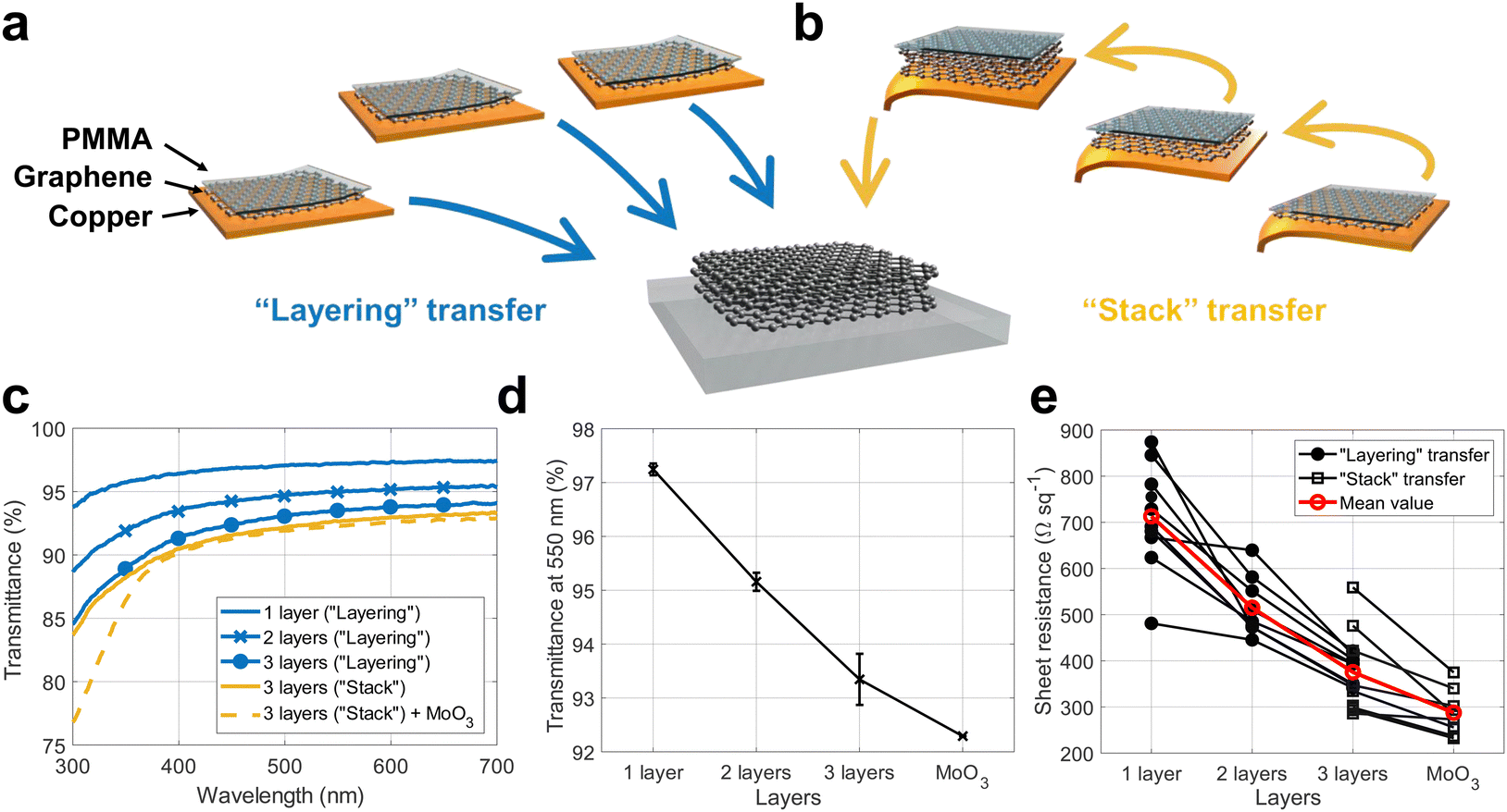 | ||
| Fig. 2 (a) Schematic representation of the “layering” transfer approach, where each graphene layer is transferred onto the target substrate, and (b) the “stack” transfer, where each additional layer of graphene is “picked up” from its catalytic Cu substrate by the previous layers and then, once complete, the entire multilayer stack is transferred to the target substrate. (c) Optical transmittance spectra of single, double and three-layer graphene (by both transfer approaches), and of three-layer graphene after evaporation of 15 nm of MoO3. (d) The evolution of the optical transmittance at 550 nm with each additional graphene layer and after MoO3 evaporation (15 nm). The error bars represent the standard deviation for several equivalent samples. (e) Sheet resistance of samples with different number of graphene layers, as well as after evaporation of 15 nm of MoO3. | ||
2.3. Cellulose-based substrate preparation
The free-standing cellulose nanocrystal membranes were prepared from 2 wt% suspensions without phase separation of commercial Na neutralized spray-dried CNCs (provided by CelluForce©) in H2O, by evaporation-assisted assembly at room temperature. To this end, these dispersions were further diluted (3 g of CNCs suspension in 5 g of H2O for each membrane) and poured into polystyrene Petri dishes (5 cm diameter), resulting in membranes which can be easily separated from the dish after evaporation, becoming completely free-standing. The resulting membranes presented a thickness of approximately 15–25 µm.For the transparent regenerated cellulose cigarette rolling papers the brand “aLedinha”, by aLeda, was used. The thickness of these papers was measured at ∼18 µm.
2.4. OLED fabrication
The OLED structure was based on the host:guest concept, with a reduced number of organic layers. On top of the graphene anode, a thin (15 nm, with other thicknesses also explored in this work) layer of MoO3 was deposited by thermal evaporation under high vacuum (10−5–10−6 mbar), at relatively low evaporation rates (1 Å s−1), in order to guarantee a uniform interface with graphene. The device active layer was deposited by spin coating (solution statically dispensed) at 2000 rpm for 30 seconds, after filtering the solution with a 0.1 µm polytetrafluoroethylene filter and drying in the glovebox at 80 °C for 30 min. For the active layer solution, a blend composed of (PVK:mCP) (0.7:0.3; 92 wt%):TXO-TPA (8 wt%), where the PVK (poly(N-vinylcarbazole)) and mCP (1,3-bis(N-carbazolyl)benzene) are the host constituents and the TXO-TPA (2-(4(diphenylamino)phenyl)-10,10-dioxide-9H-thioxanthen-9-one) is the guest, a TADF (thermally activated delayed fluorescent) emitter. The materials were solubilized in chlorobenzene (10 mg mL−1, for host and guest, independently) and then mixed in order to achieve the above-mentioned concentrations in the host:guest matrix. After the deposition of the active layer, the electron transport layer of TPBi (2,2′,2″-(1,3,5-Benzinetriyl)-tris(1-phenyl-1-H-benzimidazole)) with a thickness of 40 nm was thermally evaporated in the same conditions of the molybdenum oxide. Finally, a 10 nm layer of Ca was evaporated, at an evaporation rate of 1 Å s−1, followed by a thick (100 nm) layer of Al, evaporated at 2 Å s−1. Ca presents a favourable match between the cathode work function and the LUMO level of TPBi, while Al was used to avoid the typically fast Ca oxidation (in the latter). The active areas of the devices were around 7–9 mm2 for the rigid OLEDs and 2–4 mm2 for the flexible ones, the latter being smaller due to the increased handling difficulties when transferring graphene onto such substrates.
2.5. Material and device characterization
Secondary electron scanning electron microscopy (SE–SEM) images were acquired using a Vega 3 SBH system by TESCAN, with an acceleration voltage of 5 kV and a working distance of 15 mm. Raman spectroscopy was performed using a Jobin Yvon HR800 Raman system, by Horiba, and a He–Cd 441.6 nm laser by Kimmon. Sheet resistance measurements were performed by the van der Pauw method, using a Keysight B2902A dual-channel source meter unit and a computer-controlled multiplexer. Transmittance and reflectance spectra were acquired using a Shimadzu UV-3600 UV-vis-NIR spectrophotometer. AFM measurements were performed with a PARK XE7 atomic force microscope, in non-contact mode, with a PPP-NCHR standard non-contact tapping mode AFM probe. The probe had a standard beam shaped cantilever with a 30 nm thick reflex aluminium coating. The cantilever had a force constant of 42 N m−1, length of 125 µm, width of 30 µm and thickness of 4 µm. The selected frequency for measurement was 304 kHz. The probe radius was <10 nm.The current density–voltage–luminance (J–V–L) characteristics were determined using a Keithley 2425 source meter unit and a Konica Minolta LS-100 Chromameter. For the electroluminescence spectra measurements, an Ocean Optics USB4000 spectrometer was used. The OLED efficiencies were calculated considering that the emission follows a Lambertian emitter.
3. Results and discussion
3.1. CVD graphene transparent electrodes
Before considering any application of CVD graphene it is important to achieve good control over its synthesis. Here, characteristics such as number of layers, nucleation density and uniformity are the most important ones, as they have a direct influence on graphene's properties. In a previous work we demonstrated that the nucleation density and the presence of secondary layers (adlayers) depend, among other variables, on the carbon impurities present in the copper substrate.28 To overcome this, an in situ oxidation/reduction treatment of the substrate was performed prior to the regular CVD process, by allowing air inside the reaction chamber at high temperature, followed by a reduction in H2 atmosphere. This, aided by other tweaks to the growth recipe (Fig. 1a), resulted in the formation of millimeter-sized, sparsely distributed hexagonal graphene domains with improved charge carrier mobility. For this work, this growth recipe was adapted in order to achieve complete coverage of the substrate by promoting the coalescence of the individual graphene domains, at the expense of a slightly higher nucleation density (and, consequently, higher density of grain boundaries). The Raman spectra (with a representative one, this time on a fused silica substrate, in Fig. 1b) reveal additional information about the obtained material. The sharp and narrow G and 2D peaks, with a high intensity ratio of I2D/IG ≈ 2, are typical of single-layer graphene (SLG). Moreover, the absence of the D peak (typically at 1370 cm−1 for 442 nm excitation wavelength) is indicative of the absence of defects in its crystalline structure. As for the microscopic morphology of this material, secondary electron scanning electron microscopy (SE-SEM) images (Fig. 1c) reveal a mostly uniform film with some wrinkles, which are typical in CVD grown graphene.29 Some small white features can also be observed, attributed to silicates, which are known to occur during CVD of graphene due to the silica contamination from the quartz walls of CVD reactors.30,31 Occasionally, some secondary layers can also be seen across the samples, due to their darker contrast relative to the underlying film. These usually assume either a flower-like shape (Fig. 1d), referencing the six-fold symmetry of the graphene domains, or a more dendritic form, with further adlayers in the middle (Fig. 1e). Importantly, these secondary layers are sporadic, as can be seen at low magnifications (Fig. S1, ESI†).A good transparent conductive material should combine low electrical resistance with high optical transparency. In the case of one of the most used TCMs, ITO, the sheet resistance is typically ∼10 Ω sq−1,17 while its transmittance at 550 nm (the typically employed reference wavelength, roughly corresponding to the region of highest sensitivity of the human eye to visible light) is around 90%.17 Single-layer CVD graphene typically presents a much larger sheet resistance (500–1000 Ω sq−1), but benefits from higher optical transparency, showing a mostly flat absorption of ∼2.3% in the visible part of the spectrum.19 As such, a commonly employed strategy to produce CVD graphene-based transparent electrodes capable of competing with ITO is to stack, by successive transfers, multiple graphene layers (usually 3 or 4) on top of each other. Additionally, in many cases the graphene must be doped, typically by charge transfer approaches.21,32–37 This is done not only to further reduce the sheet resistance of this TCM, but also, in the case of OLED applications, to change the work function of graphene and thus ensure better charge injection into the device, through a more favourable energy level alignment.
Here, we performed the stacking of three graphene layers by two different strategies, followed by thermal evaporation of MoO3, which is known to induce p-type doping in graphene.38,39 In the first transfer approach (the “layering” transfer), each graphene layer is transferred onto the target substrate in succession, after the PMMA support layer from the previous transfer is removed (Fig. 2a). The second approach (the “stack” transfer) consists in transferring the graphene layers onto a copper substrate where another graphene film was grown and then, once a three-layer stack is complete, transferring it to the target substrate (Fig. 2b). This strategy has the advantage of requiring only one PMMA support layer throughout the entire process, reducing the transfer time and avoiding the trapping of PMMA residues between the graphene layers.
The effect of each additional layer, transferred by the “layering” approach, on the optical transmittance of the resulting graphene TCM is shown in Fig. 2c (blue lines). As can be seen, the overall transparency decreases with each additional layer (Fig. 2d). Additionally, a transmittance spectrum corresponding to a three-layer sample obtained by the “stack” transfer is presented (yellow line in Fig. 2c), and, interestingly, its transparency is slightly lower than for the three-layer sample obtained by the “layering” approach. This can be explained by a higher density of holes and tears in the “layering” films, as in this case we expect more impurities to be trapped between the layers, compromising the structural integrity of the films. Finally, after the evaporation of 15 nm of MoO3 on top of a three-layer sample obtained by the “stack” transfer approach, there is a very small decrease in the transmittance (dashed yellow line in Fig. 2c). Importantly, its value is 92.7% at 550 nm, which is above the typical requirement of 90% for TCMs, and no new features can be seen in the spectrum (Fig. 2d).
Fig. 2e shows the evolution of the sheet resistance of various equivalent samples for different numbers of layers (both transfer approaches are included), as well as after the evaporation of a 15 nm thick layer of MoO3 on top of the three-layer graphene “stack” films. While there is a fairly large spread of sheet resistance (RS) values, a clear trend can be seen as the average RS decreases from 713 to 375 Ω sq−1. Furthermore, the doping effect of the evaporated MoO3 layer can be confirmed, as RS decreases from 375 to 288 Ω sq−1 after the evaporation. This agrees well with previous reports of MoO3 evaporation on top of graphene as p-doping agent.39 The large difference between graphene and MoO3 the work functions (ϕ(graphene) = 4.2 – 4.5 eV and ϕ(MoO3) ≈ 6.7 eV) creates a charge transfer state from graphene to MoO3 layer, due to its high electron affinity. This transfer promotes the graphene's Fermi level alignment with the MoO3's conduction band edge, shifting the graphene's Fermi level close to the oxide's valence band. As a consequence of that, a better match of energy levels required for hole injection (5.3 eV) is created. Besides that, this charge transfer process decreases the graphene sheet resistance, as we experimentally observed. It is also important to highlight that while the sheet resistance typically obtained for ITO on rigid substrates is considerably lower, the relevant comparison is with thin ITO films on flexible substrates, where the lower thickness of the films increases the sheet resistance. The values obtained here are sufficiently low to enable the operation of OLEDs, as is discussed below.
3.2. Thermally activated delayed fluorescence OLEDs on Quartz
Next, we employed the graphene films obtained by “stack” transfer (as this approach is faster and results in fewer PMMA residues) and MoO3 doping as anodes in thermally activated delayed fluorescence (TADF) OLEDs on quartz substrates. The effect of varying thickness of MoO3 (10, 15, 20 and 30 nm) on the performance of the devices was evaluated. The chosen emitter was the yellow-orange TADF 2-(4(diphenylamino)phenyl)-10,10-dioxide-9H-thioxanthen-9-one (TXO-TPA) in a solution-processable host mixture of poly(N-vinylcarbazole) and 1,3-bis(N-carbazolyl)benzene (PVK:mCP). This enables a device structure with reduced complexity (Fig. 3a), as the chosen host can efficiently transfer the electrical charge to the emitter (guest), while also allowing (due to the mixed effect of both PVK and mCP) a better balance of electron and hole mobilities. The emissive layer (EML) was spin coated on top of the thermally evaporated MoO3, followed by further evaporation of 40 nm of 2,2′,2″-(1,3,5-benzinetriyl)-tris(1-phenyl-1-H-benzimidazole) (TPBi) electron transport layer (ETL), with an electron mobility in the range of 3.3–8 × 10⁻⁵ cm2 V−1 s−1.40 The device was completed by an anode consisting of thermally evaporated Ca (10 nm) and Al (100 nm). The entire structure of the OLED can be summarized as quartz/graphene (3 layers)/MoO3 (different thicknesses)/PVK:mCP:TXO-TPA (∼50 nm)/TPBi (40 nm)/Ca (10 nm)/Al (100 nm). As such, the OLEDs have only two organic layers. | ||
| Fig. 3 (a) Schematic representation of the OLED structure on quartz substrates. Different thicknesses of MoO3 were explored (x = 10, 15, 20 and 30 nm). (b) Current density and brightness of the OLEDs with different thicknesses of MoO3, as a function of applied voltage. (c) Current (ηC), power (ηP) and external quantum efficiencies of OLEDs with different thicknesses of MoO3, as a function of brightness. (d) Current density versus voltage of OLEDs with different thicknesses of MoO3, fitted to the space charge current limit (SCLC) model. | ||
Fig. 3b shows the current density and luminance of the OLEDs as a function of voltage (a photograph of one of these devices can be seen in Fig. S2, ESI†). As can be seen, all the devices show a turn-on voltage of 3 V, except for the one with 10 nm of MoO3 (3.5 V). This indicates that the increase in the thickness of MoO3 does not significantly increase the energy barrier for the injection of holes, meaning that the energy band alignment (and, consequently, the graphene doping) does not change with the thickness of MoO3 (within the range explored here). Moreover, this turn-on voltage is slightly lower than the ones reported previously for devices employing ITO/PEDOT:PSS anodes.41 As the work function of MoO3 is usually larger compared to PEDOT:PSS,42 the energy barrier for hole injection into HOMO level of the host:guest matrix is slightly lower in our devices, justifying the lower turn-on voltage (3 V). As for the brightness, the device with 15 nm of MoO3 achieves the highest value (Lmax = 920 cd m−2), which is fairly stable over a wide range of voltages. The current density, however, increases steadily, ultimately resulting in an external quantum efficiency (EQE) that drops progressively (as a function of brightness) from the maximum value of 1.20% (L = 221 cd m−2@5.5 V) to 0.53% (Lmax@10.5 V), exhibiting roll-off losses of about 50% (Fig. 3c). This data is not surprising in OLEDs employing TXO-TPA emitter and can be related to some possible triplet–triplet annihilation (TTA), as previously indicated.41 Larger thicknesses of MoO3 achieve lower EQE values (<1%), with strong oscillations in their brightness curves. This might be caused by the morphology of the oxide layer, with an increase in the density of defects for larger thicknesses. In order to understand the impact of MoO3 thickness on the charge carrier transport in quartz-supported OLEDs, we can make an analysis under the space-charge-limited current (SCLC) model in the J–V data (Fig. 3d), according to the Child's law:43
 | (1) |
nm) = 1.43 × 10⁻⁶ > µ(10nm) = 1.27 × 10⁻⁶ > µ(15nm) = 1.22 × 10⁻⁶ > µ(20nm) = 9.95 × 10⁻⁷ cm2 V−1 s−1. Looking at these electrical mobility values, the SCLC goodness of fit, quality of J, L × V curves and correlating with the performance of the OLEDs (Fig. 3), we chose the MoO3 thickness of 15 nm for the flexible cellulose-supported OLEDs that are discussed further below.
3.3. Cellulose-based substrates for OLEDs
For the flexible OLEDs we explored two cellulose-based substrates: cellulose nanocrystal (CNC) membranes and commercial transparent cigarette rolling papers. Besides being naturally derived and biodegradable, both substrates possess additional advantages that make them well suited as ESI† for environmentally friendly OLEDs. The CNC membranes, thanks to the nanometric size and packing of the cellulose crystals, allow to obtain very low surface roughness (nanometer range), while conventional paper presents values in the micrometer range.48 Moreover, under the proper drying conditions, CNC substrates are able to self-organize in chiral structures that may present very interesting optical properties, such as structural colour, a photonic bandgap, and, due to intrinsic left-handedness of such structures, the capability of interacting selectively with left and right circular polarized light. This, however, is dependent on the used phase, and thus requires phase separation of the CNC aqueous suspension before the preparation of the membranes. The CNC substrates used here were produced with a mixture of anisotropic and isotropic phases. As for the rolling papers, these are made from cellophane and glycerine, not only possessing relatively high smoothness, but also being extremely transparent and flexible. Fig. 4a shows transmittance spectra of CNC and rolling paper used in this work (where it should be noted that both substrates have similar thicknesses, with CNC in the range of 15–25 µm and rolling paper at ∼18 µm). The CNC membrane has decreased transmittance at ∼550 nm. This is due to the photonic bandgap of this material.49,50 The rolling paper, on the other hand, shows a good transmittance over the entire visible wavelength range. Additionally, to confirm that the surface morphology of these cellulose-based substrates is suitable for OLED applications, we performed atomic force microscopy measurements (Fig. 4b and c). The CNC membrane had a root mean square (rms) surface roughness of ∼13 nm, while for the rolling paper the value was ∼15 nm. In the case of the rolling paper, one can see a granular morphology, with small particles on the surface which may originate from either the manufacturing process or from environmental contaminations (they are not, however, visible by scanning electron microscopy, Fig. S3, ESI†). These may be detrimental, as they can cause short-circuits between the anode and the cathode. Nonetheless, both materials show a surface roughness low enough for OLED applications. To evaluate the suitability of cellulose membranes as substrates for supporting graphene electrodes in optoelectronic applications, AFM images of CNC/PMMA/graphene samples were obtained (Fig. S4, ESI†). The images reveal a surface roughness comparable in magnitude to that observed for the CNC membrane (≈12.44 ± 4.37 nm). These results confirm that cellulose-based substrates can be effectively utilized as supports for lighting devices. | ||
| Fig. 4 (a) Transmittance spectra of the CNC and RP substrates. (b) AFM images of CNC and (c) RP substrates, with the root mean square roughness values. (d) Schematic representation of the modified transfer of graphene onto cellulose-based substrates. | ||
To reduce the exposure of these substrates to water, which can result in uneven swelling (or, in the case of CNC, complete breakdown of the membrane), we modified the typical wet transfer process of graphene (Fig. 4d). The “stack” approach was taken as the starting point, as it has the advantage of introducing the substrate only at the very end of the process. After the electrochemical delamination of the three-layer graphene, previously cut in the shape of a narrow conductive track (∼2–3 mm wide), the graphene + PMMA film is scooped out with a polytetrafluoroethylene (PTFE) plate. Immediately after, the target substrate (either CNC or rolling paper) is briefly wet in water and placed on top of the PTFE plate, covering the graphene. The entire assembly is then left to dry in air, in ambient conditions. Finally, once dried, the cellulose-based substrate is removed from the PTFE, with the graphene + PMMA sticking to the substrate (as the adhesion of graphene to PTFE is very low). This results in a substrate + PMMA + graphene stack, which can then move on to the MoO3 deposition stage.
3.4. Flexible OLEDs on cellulose-based substrates
The flexible OLEDs were fabricated with the following structure: cellulose substrate/PMMA/graphene (3 layers)/MoO3 (15 nm)/PVK:mCP:TXO-TPA (∼50 nm)/TPBi (40 nm)/Ca (10 nm)/Al (100 nm) (Fig. 5a). OLEDs made on both types of substrates (designated as CNC-OLED and RP-OLED, for CNC and rolling paper substrates, respectively) show visible light emission under applied voltage, as seen in Fig. 5b for RP-OLED, which continues to operate even under fairly extreme bending and twisting. In contrast, the CNC-OLED (Fig. S5, ESI†), while allowing some degree of flexibility, is far more brittle. Fig. 5c shows representative electroluminescence spectra of the obtained OLEDs. In both cases, the maximum of electroluminescence spectra is near 560 nm, characteristic of TXO-TPA, with a small band at ∼400 nm, corresponding to the PVK host. The latter is particularly common when the energy (electrical carriers) transfer from the host to the guest is not achieved completely.47Fig. 5d shows the current density and brightness of CNC-OLED and RP-OLED as a function of voltage. Similar to the devices on quartz, the turn-on voltage is around 3 V, indicating that the energy levels are still well aligned, independently of the substrate. The maximum brightness of RP-OLED, at ∼400 cd m−2, is four times larger than that of CNC-OLED (∼100 cd m−2). Moreover, the current density of RP-OLED is also larger than for CNC-OLED at the same brightness. As such, the maximum current and power efficiencies are higher for RP-OLED, at 0.4 cd A−1 and 0.3 lm W−1, respectively (versus 0.2 cd A−1 and 0.2 lm W−1 for CNC-OLED), as seen in Fig. 5e. The EQE is also higher for RP-OLED, with a value of 0.34% (versus 0.17% for CNC-OLED). We also note the earlier onset of efficiency roll-off for CNC-OLED (Fig. 5f). | ||
| Fig. 5 (a) Schematic representation of the OLED structure on the cellulose-based substrates. (b) Photographs of RP-OLED emitting light, even under considerable bending. (c) Electroluminescence spectra of CNC-OLED and RP-OLED. (d) Current density and brightness of the OLEDs on cellulose-based substrate, as a function of applied voltage. (e) Current (ηC), power (ηP) and external quantum efficiencies of the cellulose-supported OLEDs and (f) their efficiency roll-off, as a function of brightness. (g) Current density versus voltage of CNC-OLED and RP-OLED, fitted to the SCLC model, where CL corresponds to the Child's law regime and J ∝ Vn to the Mark-Helfrich domain, with the Mott-Gurney regime at low voltages. | ||
We begin the analysis of these devices by exploring the charge-carrier transport features in shallow- and deep-trap SCLC behaviour, as well as after the trap-filling process (Child's law) (Fig. 5g). Charge-carrier mobility from Child's model suffers a direct impact of densities of trap defects (Nt) and free-carriers (n0), during the trap-filling process (Mott-Gurney model).51 Taking into account this characteristic, eqn (1) can be rewritten in terms of the effective mobility (µeff):
 | (2) |
 | (3) |
In this context, the obtained effective electrical mobilities for RP and CNC-OLEDs are 3.14 × 10⁻⁹ and 3.85 × 10⁻⁹ cm2 V−1 s−1, respectively. It should be noted that, in the whole device, we are calculating the electrical mobility of the slowest electrical carrier (that, in almost all of the organic materials employed in these OLEDs, is the electron). On the other hand, electrical mobilities after the trap-filling process (under Child's law domain) have values about 103 times higher than the ones under shallow-trap SCLC conditions, with µSCLC(RP) = 5.11 × 10⁻⁶ cm2 V−1 s−1 and µSCLC(CNC) = 4.16 × 10⁻⁶ cm2 V−1 s−1. Thus, the density of trap defects parameters (θ0) for RP and CNC are 6.14 × 10⁻⁴ and 9.25 × 10⁻⁴, respectively. Applying Mark-Helfrich's equation,52 in the deep-trap filling behaviour (between shallow-trap and Child's law domain) to calculate the average energy of trap-states (Et) for each OLED, we obtain Et(RP) = 280 meV and Et(CNC) = 252 meV. These values are similar and typical of shallow defects.
The voltage where the Mott-Gurney regime transitions into the Mark-Helfrich domain, designated as the trap-filling limit voltage (VTFL), allows to obtain the total density of trap defects (Nt) by combining the equations corresponding to these two domains:
 | (4) |
At the same time, one cannot disregard the effect of the optical outcoupling, which, considering the transmittance spectra of both substrates (Fig. 4a), could be expected to be better in RP-OLEDs compared to CNC-OLEDs. However, there might be a possible underestimation of the brightness due to the photonic bandgap reflection in the CNC, which can result in a deviation from the Lambertian emission profile. If the photons reflected in this substrate are emitted at an angle away from the normal direction (used for brightness measurement in this work), the total measured brightness will be underestimated. In this hypothesis, the CNC-OLED figures of merit would be slightly better than the ones that we obtain here. On the other hand, if there is total internal reflection, photon loss is expected, justifying the lower performance of CNC-OLED.
4. Conclusions
We explored the use of CVD graphene in flexible OLEDs on cellulose nanocrystal membranes and transparent rolling papers. The graphene anodes, with a sheet resistance of 288 Ω sq−1, were obtained using an optimized CVD recipe, multiple layer stacking and charge transfer doping by MoO3. The effect of the MoO3 thickness on the performance of solution processed TADF OLEDs was also investigated, with a film of 15 nm resulting in the best performing device in terms of stability of maximum brightness. Finally, we applied these findings to fabricate cellulose-supported OLEDs, after appropriate adaptations of the graphene transfer process to these water-sensitive substrates. Despite the modest external quantum efficiencies, as well as low current and power efficiencies (0.34%, 0.4 cd A−1 and 0.3 lm W−1, respectively, in the best case), these devices demonstrate for the first time the combined potential of graphene and cellulose-based substrates for flexible environmentally conscious optoelectronic applications.Author contributions
Bohdan Kulyk (conceptualization: lead; investigation: lead; methodology: lead; visualization: lead; writing – original draft: lead; writing – review & editing: lead). José C. Germino (conceptualization: equal; investigation: equal; methodology: equal; visualization: equal; writing – original draft: supporting; writing – review & editing: equal). Diana Gaspar (conceptualization: supporting; investigation: supporting; resources: supporting; writing – original draft: supporting; writing – review & editing: equal). António J. S. Fernandes (conceptualization: equal; investigation: equal; methodology: equal; resources: equal; supervision: supporting; writing – review & editing: equal). Jonas Deuermeier (investigation: supporting; writing – review & editing: equal). Alexandre F. Carvalho (conceptualization: supporting; investigation: supporting; visualization: supporting; writing – review & editing: equal). António F. da Cunha (investigation: supporting; writing – review & editing: equal). Luís M. N. Pereira (conceptualization: equal; methodology: supporting; resources: supporting; supervision: equal; writing – review & editing: equal). Luiz Pereira (conceptualization: equal; funding acquisition: equal; investigation: supporting; methodology: equal; resources: supporting; software: supporting; supervision: equal; writing – original draft: supporting; writing – review & editing: equal). Florinda M. Costa (conceptualization: equal; funding acquisition: equal; methodology: equal; resources: equal; supervision: lead; writing – review & editing: equal).Data availability
The data that supports the findings of this study is available in the manuscript and its ESI.†Conflicts of interest
The authors declare no conflict of interest.Acknowledgements
This work was developed within the scope of project i3N (LA/P/0037/2020, UIDB/50025/2020 and UIDP/50025/2020), financed by national funds through the Portuguese Foundation for Science and Technology/MCTES (FCT I.P.). B. Kulyk acknowledges the PhD grant SFRH/BD/141525/2018 from FCT I.P. J. C. Germino acknowledges FCT/i3N/UA for the individual CEEC grant (2021.02056.CEECIND). D. Gaspar, and L. Pereira would like to acknowledge FCT – Portuguese Foundation for Science and Technology under the project CELLECTIVE (PTDC/CTM-CTM/4653/2021). The authors also thank Maria João Sá Pereira for the AFM measurements. Helpful discussions with Prof. Caroline Murawski and with Jorge Moura are also gratefully acknowledged.References
- S.-J. Zou, Y. Shen, F.-M. Xie, J.-D. Chen, Y.-Q. Li and J.-X. Tang, Mater. Chem. Front., 2020, 4, 788 RSC.
- C. Keum, C. Murawski, E. Archer, S. Kwon, A. Mischok and M. C. Gather, Nat. Commun., 2020, 11, 6250 CrossRef CAS PubMed.
- T. Wang, Y.-Z. Wang, L.-C. Jing, Q. Zhu, A. S. Ethiraj, W. Geng, Y. Tian, Z. Zhu, Z. Meng and H.-Z. Geng, Carbon, 2021, 172, 379 CrossRef CAS.
- E. Fortunato, N. Correia, P. Barquinha, L. Pereira, G. Goncalves and R. Martins, IEEE Electron Device Lett., 2008, 29, 988 Search PubMed.
- R. Martins, D. Gaspar, M. J. Mendes, L. Pereira, J. Martins, P. Bahubalindruni, P. Barquinha and E. Fortunato, Appl. Mater. Today, 2018, 12, 402 CrossRef.
- B. Kulyk, B. F. R. Silva, A. F. Carvalho, S. Silvestre, A. J. S. Fernandes, R. Martins, E. Fortunato and F. M. Costa, ACS Appl. Mater. Interfaces, 2021, 13, 10210 CrossRef CAS PubMed.
- B. Kulyk, B. F. R. Silva, A. F. Carvalho, P. Barbosa, A. V. Girão, J. Deuermeier, A. J. S. Fernandes, F. M. L. Figueiredo, E. Fortunato and F. M. Costa, Adv. Mater. Technol., 2022, 2101311 CrossRef CAS.
- B. Kulyk, M. Matos, B. F. R. Silva, A. F. Carvalho, A. J. S. Fernandes, D. V. Evtuguin, E. Fortunato and F. M. Costa, Diamond Relat. Mater., 2022, 123, 108855 CrossRef CAS.
- B. Kulyk, S. O. Pereira, A. J. S. Fernandes, E. Fortunato, F. M. Costa and N. F. Santos, Carbon, 2022, 197, 253 CrossRef CAS.
- T. Pinheiro, S. Silvestre, J. Coelho, A. C. Marques, R. Martins, M. G. F. Sales and E. Fortunato, Adv. Mater. Interfaces, 2021, 2101502 CrossRef CAS.
- S. H. Min, C. K. Kim, H. N. Lee and D. G. Moon, Mol. Cryst. Liq. Cryst., 2012, 563, 159 CrossRef CAS.
- Q. Zheng, H. Li, Y. Zheng, Y. Li, X. Liu, S. Nie, X. Ouyang, L. Chen and Y. Ni, J. Mater. Chem. C, 2021, 9, 4496 RSC.
- S. Purandare, E. F. Gomez and A. J. Steckl, Nanotechnology, 2014, 25, 094012 CrossRef CAS PubMed.
- M. Morales-Masis, S. De Wolf, R. Woods-Robinson, J. W. Ager and C. Ballif, Adv. Electron. Mater., 2017, 3, 1600529 CrossRef.
- A. Kumar and C. Zhou, ACS Nano, 2010, 4, 11 CrossRef CAS PubMed.
- Y. Chen, Y. Yue, S. Wang, N. Zhang, J. Feng and H. Sun, Adv. Electron. Mater., 2019, 5, 1900247 CrossRef CAS.
- A. E. Adetayo, T. N. Ahmed, A. Zakhidov and G. W. Beall, Adv. Opt. Mater., 2021, 9, 2002102 CrossRef CAS.
- C. Stampfer, F. Haupt, T. Taniguchi, M. Schmitz, L. Banszerus, K. Watanabe, M. Oellers, J. Dauber, S. Engels and B. Beschoten, Sci. Adv., 2015, 1, e1500222 CrossRef PubMed.
- R. R. Nair, P. Blake, A. N. Grigorenko, K. S. Novoselov, T. J. Booth, T. Stauber, N. M. R. Peres and A. K. Geim, Science, 2008, 320, 1308 CrossRef CAS PubMed.
- C. Lee, X. Wei, J. W. Kysar and J. Hone, Science, 2008, 321, 385 CrossRef CAS PubMed.
- L.-P. Ma, Z. Wu, L. Yin, D. Zhang, S. Dong, Q. Zhang, M.-L. Chen, W. Ma, Z. Zhang, J. Du, D.-M. Sun, K. Liu, X. Duan, D. Ma, H.-M. Cheng and W. Ren, Proc. Natl. Acad. Sci. U. S. A., 2020, 117, 25991 CrossRef CAS PubMed.
- J. O. Hwang, J. S. Park, D. S. Choi, J. Y. Kim, S. H. Lee, K. E. Lee, Y. H. Kim, M. H. Song, S. Yoo and S. O. Kim, ACS Nano, 2012, 6, 159 CrossRef CAS PubMed.
- J.-W. Shin, H. Cho, J. Lee, J. Moon, J.-H. Han, K. Kim, S. Cho, J.-I. Lee, B.-H. Kwon, D.-H. Cho, K. M. Lee, M. Suemitsu and N. S. Cho, Opt. Express, 2018, 26, 617 CrossRef CAS PubMed.
- L. Liu, W. Shang, C. Han, Q. Zhang, Y. Yao, X. Ma, M. Wang, H. Yu, Y. Duan, J. Sun, S. Chen and W. Huang, ACS Appl. Mater. Interfaces, 2018, 10, 7289 CrossRef CAS PubMed.
- T. H. Han, Y. Lee, M. R. Choi, S. H. Woo, S. H. Bae, B. H. Hong, J. H. Ahn and T. W. Lee, Nat. Photonics, 2012, 6, 105 CrossRef CAS.
- Y. Han, L. Zhang, X. Zhang, K. Ruan, L. Cui, Y. Wang, L. Liao, Z. Wang and J. Jie, J. Mater. Chem. C, 2014, 2, 201 RSC.
- T.-H. Han, M. Park, S. Kwon, S. Bae, H. Seo, H. Cho, J. Ahn and T. Lee, NPG Asia Mater., 2016, 8, e303 CrossRef CAS.
- B. Kulyk, A. F. Carvalho, A. J. S. Fernandes and F. M. Costa, Carbon, 2020, 169, 403 CrossRef CAS.
- W. J. Zhu, T. Low, V. Perebeinos, A. A. Bol, Y. Zhu, H. G. Yan, J. Tersoff and P. Avouris, Nano Lett., 2012, 12, 3431 CrossRef CAS PubMed.
- S. Al-Kamiyani and T. Mohiuddin, AIP Adv., 2018, 8, 125325 CrossRef.
- Y. Çelik, W. Escoffier, M. Yang, E. Flahaut and E. Suvacı, Carbon, 2016, 109, 529 CrossRef.
- S. J. Kwon, T. H. Han, T. Y. Ko, N. Li, Y. Kim, D. J. Kim, S. H. Bae, Y. Yang, B. H. Hong, K. S. Kim, S. Ryu and T. W. Lee, Nat. Commun., 2018, 9, 1 CrossRef CAS PubMed.
- I.-J. Park, T. I. Kim, T. Yoon, S. Kang, H. Cho, N. S. Cho, J.-I. Lee, T.-S. Kim and S.-Y. Choi, Adv. Funct. Mater., 2018, 28, 1704435 CrossRef.
- G. V. Bianco, A. Sacchetti, A. Milella, M. Grande, A. D’Orazio, P. Capezzuto and G. Bruno, Carbon, 2020, 170, 75 CrossRef CAS.
- A. E. Mansour, M. M. Said, S. Dey, H. Hu, S. Zhang, R. Munir, Y. Zhang, K. Moudgil, S. Barlow, S. R. Marder and A. Amassian, Adv. Funct. Mater., 2017, 27, 1602004 CrossRef.
- J. H. Heo, D. H. Shin, D. H. Song, D. H. Kim, S. J. Lee and S. H. Im, J. Mater. Chem. A, 2018, 6, 8251 RSC.
- L. Liu, R. Dong, D. Ye, Y. Lu, P. Xia, L. Deng, Y. Duan, K. Cao and S. Chen, ACS Appl. Mater. Interfaces, 2021, 13, 12268 CrossRef CAS PubMed.
- E. Cho, S. Cha, Y. Kim and C. Kim, Org. Electron., 2020, 77, 105437 CrossRef CAS.
- J. Meyer, P. R. Kidambi, B. C. Bayer, C. Weijtens, A. Kuhn, A. Centeno, A. Pesquera, A. Zurutuza, J. Robertson and S. Hofmann, Sci. Rep., 2014, 4, 5380 CrossRef CAS PubMed.
- W.-Y. Hung, T.-H. Ke, Y.-T. Lin, C.-C. Wu, T.-H. Hung, T.-C. Chao, K.-T. Wong and C.-I. Wu, Appl. Phys. Lett., 2006, 88, 064102 CrossRef.
- M. Kumar and L. Pereira, Nanomaterials, 2020, 10, 101 CrossRef CAS PubMed.
- M. Vasilopoulou, A. M. Douvas, D. G. Georgiadou, L. C. Palilis, S. Kennou, L. Sygellou, A. Soultati, I. Kostis, G. Papadimitropoulos, D. Davazoglou and P. Argitis, J. Am. Chem. Soc., 2012, 134, 16178 CrossRef CAS PubMed.
- N. F. Mott and R. W. Gurney, Electronic Processes in Ionic Crystals, 2nd edn, Oxford University Press, London, UK, 1948 Search PubMed.
- M. Pope and C. E. Swenberg, Electronic Processes in Organic Crystals and Polymers, Oxford University Press, 1999 Search PubMed.
- J. C. Germino, L. G. T. A. Duarte, R. A. Mendes, M. M. Faleiros, A. de Morais, J. N. de Freitas, L. Pereira and T. D. Z. Atvars, Nanomaterials, 2022, 12, 2497 CrossRef CAS PubMed.
- E. S. Moraes, L. G. T. A. Duarte, F. S. Rodembusch, J. C. Germino, L. F. R. Pereira and T. D. Z. Atvars, Mater. Adv., 2024, 5, 7778–7788 RSC.
- M. Kumar, Highly Efficient Organic Light Emitting Diodes Based on Thermally Activated Delayed Fluorescent Materials, University of Aveiro, 2019 Search PubMed.
- P. Grey, S. N. Fernandes, D. Gaspar, J. Deuermeier, R. Martins, E. Fortunato, M. H. Godinho and L. Pereira, ACS Appl. Electron. Mater., 2020, 2, 426 CrossRef CAS.
- P. Grey, Cellulose Nanocrystal Chiral Structures for Electronics and Photonics, NOVA University of Lisbon, 2021.
- M. V. Santos, A. Tercjak, J. Gutierrez, H. S. Barud, M. Napoli, M. Nalin and S. J. L. Ribeiro, Carbohydr. Polym., 2017, 168, 346 CrossRef CAS PubMed.
- L. Pereira, Organic Light Emitting Diodes: the Use of Rare Earth and Transition Metals, Pan Stanford Publishing, Boca Raton, FL, USA, 2012 Search PubMed.
- P. Zhang, Y. S. Ang, A. L. Garner, Á. Valfells, J. W. Luginsland and L. K. Ang, J. Appl. Phys., 2021, 129, 100902 CrossRef CAS.
Footnote |
| † Electronic supplementary information (ESI) available. See DOI: https://doi.org/10.1039/d4tc05137h |
| This journal is © The Royal Society of Chemistry 2025 |