
 Open Access Article
 This Open Access Article is licensed under a
 Creative Commons Attribution 3.0 Unported Licence
Proximity effects in the graphene–Co3Sn2S2 interface
Jiaxin
Zhang
a,
Beate
Paulus
b,
Yuriy
Dedkov
 *c and
Elena
Voloshina
*db
*c and
Elena
Voloshina
*db
aDepartment of Physics, Shanghai University, 99 Shangda Road, 200444 Shanghai, P. R. China
bInstitut für Chemie und Biochemie, Freie Universität Berlin, Arnimallee 22, 14195 Berlin, Germany
cInstitute of Physics, Center for Advanced Laser Techniques, Bijenička Cesta 46, 10000 Zagreb, Croatia. E-mail: ydedkov@ifs.hr
dRuđer Bošković Institute, Division of Theoretical Physics, Bijenička Cesta 54, Zagreb, Croatia. E-mail: Elena.Voloshina@irb.hr
First published on 24th April 2025
Abstract
In graphene, the linear dependence of the density of states on energy and the low density of these valence band states around the Fermi energy make this material an ideal candidate for the observation of the proximity effects, when it is placed in contact with other functional materials. In this work, we explore the possible effects of the magnetic proximity and charge transfer on the interfacial properties of a graphene layer adsorbed on the (001) surface of Co3Sn2S2, the bulk phase of which is known as a topological quasi-2D semimetal in the half-metallic ferromagnetic state. Both counterparts mutually influence the properties of the heterostructure. Thus, formation of the interface allows tuning the electronic and magnetic properties of graphene over a wide range depending on the composition of the Co3Sn2S2 interface layer. A synergy between graphene and Co3Sn2S2(001) enhances the perpendicular magnetic anisotropy energy of the systems, which is highly promising for the development of new magnetic recording media. As a reference for future experimental studies, the C 1s core-level shifts and C K near-edge X-ray absorption fine structure spectra are calculated for all considered cases.
1. Introduction
The development of new heterostructures is currently one of the most important and competitive areas of research.1–4 This is due to the fact that such systems, consisting of two or more different components, are functional materials with complementary advantages that cannot be realised using a single component.5–7 Such a synergistic effect allows them to be used as important integrants in various types of devices.3,4,8–10 Seeing that the design of new generation of devices is aimed at miniaturisation and low weight, the use of two-dimensional (2D) materials in these developments comes to the forefront.2,9–14Among 2D materials, graphene occupies a special place. This is due to its unique physical properties. Many of them, including excellent charge and spin transport properties, are determined by the behaviour of graphene-derived π-states near the Fermi level, which have a linear dispersion around K points of the graphene Brillouin zone.15 At the same time, this unique electronic structure of graphene leads to some limitations for application of this material in real electronic and spintronic devices.16,17 Yet, the low density of the valence band states (DOS) of graphene around the Fermi energy (EF) and the linear dependence of the DOS on energy make this material an ideal candidate for creating proximity-induced effects when placed in heterostructures with other functional materials.
In particular, studies on the magnetic proximity effect were carried out in the graphene/Ni(111)18–21 and graphene/Co(001)22–24 interfaces. The induced magnetic moment of carbon atoms due to the close contact with the ferromagnetic (FM) metal was detected by means of X-ray magnetic circular dichroism (XMCD) and spin-resolved photoemission experiments18,19,22 and confirmed by theory.24,25 This phenomenon is explained by the high degree of the π-3d hybridisation of the valence band states at the interface between graphene and the FM metal. However, as a result of such interaction, graphene loses its free-standing character26,27 and the carriers in the vicinity of the Fermi level cannot be described as massless Dirac particles. The latter limits the use of these interfaces for the design of electronic and spintronic devices.
One possible way of decoupling graphene from the underlying FM material is intercalation of different species in the graphene/FM interface,28,29 which leads, however, to the blocking of the effective magnetic coupling of graphene and FM metal with a loss of the induced magnetic order in a graphene layer. Another interesting approach to realising a graphene/FM interface with linear energy dispersion for electrons in graphene is to intercalate Mn into the graphene/Ge interface, which leads to formation of the metallic FM Mn5Ge3 layer at the graphene/Ge interface.30,31 In this system, only spin-up electrons of graphene at the K point and at EF conserve the Dirac-electron-like character and for the spin-down electrons the band gap is found at EF.30
Interestingly, in the graphene–FM heterostructures not only the graphene electronic properties can be tailored, but also the graphene layer itself can have a tremendous effect on the second material. For example, graphene coating on Co films can dramatically enhance the perpendicular magnetic anisotropy in ferromagnetic films and to induce modification of its magnetic configuration.32–36
Here, we explore the possible effects of the magnetic proximity and charge transfer on the interfacial properties of the graphene–Co3Sn2S2 heterostructure. Bulk Co3Sn2S2 is a shandite-type half-metallic ferromagnet (HMF) with a magnetic moment of ≈0.3μB per cobalt atom below Curie temperature TC ≈ 177 K.37–39 The ferromagnetic state is characterised by strong, easy-axis anisotropy favouring magnetisation in the out-of-plane direction.40 The crystal structure of Co3Sn2S2 can be viewed as a quasi-2D structure stacked along the c axis, thus allowing the bulk crystal to be cleaved perpendicular to the 〈001〉 direction. It has been experimentally shown that different surface terminations of Co3Sn2S2(001) likely determine electronic, magnetic and catalytic properties of the possible interfaces.40–42 In this work we consider the resulting surfaces, which can serve as substrates for graphene deposition. When acting as a substrate, Co3Sn2S2(001) is expected to induce new properties in the graphene overlayer. The graphene itself can also modify the properties of the underlying material. In the present work we examine the adsorption of graphene on the pristine Co3Sn2S2(001) surfaces, taking different terminations into account. Particular attention is paid to the change in the electronic and magnetic properties of both components of the graphene/Co3Sn2S2 interface. As a reference for future experimental studies, the C 1s core-level shifts and C K near-edge X-ray absorption fine structure spectra were calculated for the considered heterostructures. Comparison is made with the freestanding graphene and with the graphene/Co(001) interface.
2. Methods
Spin-polarised DFT calculations based on plane-wave basis sets of 500 eV cut-off energy were performed using the Vienna ab initio simulation package (VASP).43,44 The Perdew–Burke–Ernzerhof (PBE) exchange–correlation functional45 was employed. The electron–ion interaction was described within the projector augmented wave (PAW) method46 with C (2s, 2p), Co (3d, 4s), Sn (5s, 5p), and S (3s, 3p) states treated as valence states. Brillouin-zone integration was performed on Γ-centered symmetry reduced Monkhorst–Pack mesh using a Methfessel–Paxton smearing method of first order with σ = 0.2 eV, except for the calculations of total energies. For those calculations, the tetrahedron method with Blöchl corrections47 was used. 12 × 12 × 6 and 12 × 12 × 1 k-meshes were used for the bulk Co3Sn2S2 and the supercell Brillouin zone, respectively. Dispersion interactions were included by means of the DFT-D3 correction method.48 When necessary, the spin–orbit coupling (SOC) was taken into account. The spin quantisation axis was rotated from the xy plane (in-plane) to the z-axis (perpendicular) for MAE calculations. To get a more accurate value for MAE, the convergence criterion was raised to 10−6 eV for self-consistent calculations including SOC.The (001) Co3Sn2S2 surfaces were modelled by symmetric slabs with a vacuum gap of approximately 26 Å. The lattice constant in the lateral plane was set according to the optimised value of bulk Co3Sn2S2. In total, three pristine Co3Sn2S2(001) terminations were considered (Fig. 1b and c–e). The used supercells contain 13 layers of Co3Sn2S2(001). Thus, the slab compositions are Co3Sn−[SnS2−Co3Sn]6 and SnS2−[Co3Sn−SnS2]6 in the case of Co3Sn-termination (Fig. 1c) and SnS2-termination (Fig. 1e), respectively. The slab composition in the case of SnS–R (R = [Co3Sn−SnS2]6, Fig. 1d) is identical to SnS2–R where the terminal S-sublayers are omitted. To study the graphene/Co3Sn2S2(001) interfaces, the graphene layer was adsorbed on both sides of the slab. The used supercells have (1 × 1) lateral periodicity with respect to Co3Sn2S2(001) and a (2 × 2) lateral periodicity with respect to graphene. This way the graphene layer is uniformly stretched by about 7.8%. Yet, the free standing graphene adopting this lattice parameters retains its gapless band structure, and the Dirac point is at the Fermi energy. For each surface termination, three different models have been considered for the adsorption sites of carbon atoms (Fig. 1f–n). For all these structures the ions of the 9 middle inner layers were fixed at their bulk positions during the structural optimisation procedure, whereas the positions of all other ions were fully relaxed until forces became smaller than 0.02 eV Å−1. For comparison reasons, for selected cases thicker (consisting of 19-layers) slabs were considered and the calculated quantities (surface energies, magnetic moments) stayed unchanged as compared with the results obtained for the 13-layered slabs. Note, however, that using a number of layers less than 13 does not allow one to correctly describe the properties of the inner layers.
 | ||
| Fig. 1 (a) Hexagonal crystal structure of Co3Sn2S2 with the rhombohedral primitive cell highlighted by light green colour. The in-plain and out-of-plane lattice constants are indicated with letters a and c, respectively. (b) Schematic representation (side view) of various surface terminations of the clean Co3Sn2S2(001) surface. Two alternating layers, Co3Sn and SnS2, are shown in blue and orange shading. The layer thickness and interlayer distance are indicated with letters h and d, respectively. (c)–(e) Surface structure (top view) of the respective pristine terminations (cf. (b)): (c) Co3Sn–R, (d) SnS–R, (e) SnS2–R. All atoms lying below the topmost layer are faded. The calculated surface energy is given below each individual subplot. (f)–(n) Graphene/Co3Sn2S2(001) interfaces considered in this work as obtained when graphene is adsorbed at (f)–(h) Co3Sn–R, (i)–(k) SnS–R, (l)–(n) SnS2–R. Relative energy calculated as the difference between the total energy of the given structure and the lowest energy structure in the respective row is given below each individual subplot. | ||
To quantify the structural stability of different surface terminations, we define the surface free energy per unit cell γ as  . Here, G({Ni}) is the Gibbs free energy of the slab, and Ni with i = Co, Sn, S are the numbers of cobalt, tin, and sulfur atoms. The chemical potentials of Co (μCo), Sn (μSn), and S (μS) obey the constraint 3μCo + 2μSn + 2μS = μCo3Sn2S2, where μCo3Sn2S2 is the chemical potential of one Co3Sn2S2 formula unit in the bulk compound. Here G is replaced by the total energies from DFT calculations, neglecting contributions from configurational or vibrational entropies.49 In this approximation μCo3Sn2S2, is equal to the DFT total energy of bulk Co3Sn2S2 per primitive unit cell. μCo, μSn, μS are the chemical potentials of Co, Sn, S according to the energy per atom in the bulk Co, bulk S, and bulk Sn, respectively. The calculations for bulk Co, Sn and S were carried out with the same computational settings as for Co3Sn2S2, and the k-meshes used were 24 × 24 × 16, 8 × 8 × 14 and 4 × 4 × 2, respectively. Taking into account the slab composition in each particular case the surface energy per surface area can be written as
 | (1) |
The interaction energy between graphene and Co3Sn2S2 per C atom is defined as
 | (2) |
The Bader charge analysis50–52 was used in the calculations of charge distribution, allowing determination of the doping of graphene.
The MAE is extracted from the difference between the total energies of the two configurations – in-plane versus out-of-plane orientations of the magnetic moments:
| MAE = E|| − E⊥. | (3) |
Changes in the core level energies were estimated in the so-called final-state approximation, as follows: first, a standard calculation is performed on the fully relaxed system (bulk or slab). Then, in a subsequent calculation, an electron from the chosen core level of a particular atom is excited to the lowest conduction band, and the valence electronic structure is relaxed at fixed atomic configuration. The energy difference between these two calculations provides an estimate of the core level binding energy. This approach was previously used for graphene–metal systems and the obtained results are in good agreement with the experimental data.53
The NEXAFS spectra simulations were obtained with ELSA-software54 according to the procedure described in ref. 55 and 56. To obtain an input for the NEXAFS spectra simulations, we employed large supercells of (6 × 6) and (4 × 4) periodicity when studying free-standing graphene and gr/Co(0001) or gr/Co3Sn2S2(001) systems, respectively.
3. Results and discussion
The crystal structure of the shandite Co3Sn2S2 is displayed in Fig. 1(a). It is discussed in detail in ref. 37, 38, 57 and 58. In the context of the present study, we consider this structure as consisting of two alternating layers, each of which is stacked in the ABC sequence (Fig. 1b). One of this layers is formed by Co atoms and one of the Sn atoms (Sn1), which are organised in a hexagonal-planar structure (hCo3Sn = 0, Table 1). Another layer is formed by the second Sn atom (Sn2) which is surrounded by six S atoms in a trigonal-antiprismatic configuration. Thus, this layer consists of three sublayers (formed by Sn2 and two S atoms) and has an overall thickness of 1.321 Å (hSnS2, Table 1). The ideal vertical distance between Sn1 and Sn2 is 2.168 Å (d1 = d2, Table 1).| Co3Sn2S2 bulk | Co3Sn2S2(001) | graphene/Co3Sn2S2(001) | |||||
|---|---|---|---|---|---|---|---|
| Co3Sn–R | SnS–R | SnS2–R | Co3Sn–R | SnS–R | SnS2–R | ||
| h Co3Sn and hSnSx with x = 1 or 2 (in Å) are thicknesses of the Co3Sn and SnS2 layers, respectively (cf.Fig. 1b); d1 (in Å) is the mean distance between the surface, (S), and the subsurface, (S − 1), layers of Co3Sn2S2(001) (cf.Fig. 1b). d2 (in Å) is the mean distance between the (S − 1) and (S − 2) layers of Co3Sn2S2(001) (cf.Fig. 1b). d0 (in Å) is the mean distance between the graphene overlayer and the interface sublayer of the substrate. mbulkCo and msurfCo (in μB per atom) are magnetic moments of Co lying in the middle of the slab and in one of the surface layers, respectively. mC (in μB per atom) is an average magnetic moment of C-atoms in graphene overlayer (several values for the nonequivalent carbon atoms are indicated). γ (in meV per Å2) is the surface energy. Eint (in meV per C-atom) is the interaction energy between graphene and Co3Sn2S2(001). ΔQ (in e−1) is the charge transfer between the graphene and the substrate from the Bader charge analysis per C atom (negative value represents transfer of electron from the graphene to the substrate, i.e., p-doping of graphene). ED − EF (in eV) is the position of the Dirac point with respect to the Fermi energy. Eg (in meV) is the band gap at the Dirac point (two values are given for the spin-up and spin-down channels, respectively). MAE (in μeV per atom) is the out-of-plane magnetic anisotropy energy. | |||||||
| h Co3Sn | 0 | 0.481 | 0.104 | 0.543 | 0.374 | 0.090 | 0.498 |
| h SnSx | 1.321 | 1.439 | 0.575 | 1.470 | 1.467 | 0.554 | 1.406 |
| d 1 | 2.168 | 2.230 | 2.285 | 2.021 | 2.003 | 1.931 | 2.017 |
| d 2 | 2.168 | 2.242 | 2.100 | 2.389 | 2.188 | 2.093 | 2.361 |
| d 0 | — | — | — | — | 2.332 | 3.375 | 3.140 |
| m bulkCo | +0.340 | +0.343 | +0.343 | +0.338 | +0.341 | +0.343 | +0.337 |
| m surfCo | — | +0.168 | +0.347 | −0.020 | +0.332 | +0.338 | +0.011 |
| m C | — | — | — | — | +0.020/−0.015 | ±0.001 | 0.000 |
| γ | — | 120 | 41 | 23 | — | — | — |
| E int | — | — | — | — | −273 | −31 | −40 |
| ΔQ | — | — | — | — | +0.068 | +0.009 | −0.001 |
| E D−EF | — | — | — | — | — | −449 | +255 |
| E g | — | — | — | — | — | 66/222 | 85/61 |
| MAE | 162 | 93 | 141 | 58 | 108 | 188 | 67 |
To start our studies, we revisited the electronic properties of bulk Co3Sn2S2. The optimised lattice constants a = b = 5.3125 Å, c = 13.0009 Å and calculated magnetic moment of 0.99μB f.u.−1 are in good agreement with the experimental values a = b = 5.3680 Å, c = 13.1830 Å and 0.93μB f.u.−1,38,39 respectively. The calculated magnetic anisotropy energy (MAE) is equal to 160 μeV per Co atom, which is in good agreement with the previously published value of 190 μeV.59 [Note: the difference in the calculated values can be attributed to different computational settings used in previous and present studies.] The calculated atom-projected DOSs for the ferromagnetic bulk Co3Sn2S2 are shown in Fig. 2a. At low binding energies the valence band states are dominated by the Co 3d states weakly hybridised with Sn and S states. Below E − EF≈ − 3.5 eV the Sn 5s and S 3p states start to contribute to DOS where they effectively hybridise with Co 3d states. As can be seen from these data, bulk Co3Sn2S2 is HMF with only spin-up electrons at EF and the band gap of 0.340 eV for spin-down electrons is formed. These results are in very good agreement with previous works.38–40,57
 | ||
| Fig. 2 (a) Spin-resolved atom-projected DOSs calculated for bulk Co3Sn2S2. (b–d) Spin-resolved DOS projected on atoms occupying the two topmost surface layers of (b) Co3Sn–R; (c) SnS–R; (d) SnS2–R. | ||
The quasi-layered lattice structure of bulk Co3Sn2S2 in the xy plane (Fig. 1b) makes it easy to obtain the (001) surface in experiments. At that, three surface terminations are possible: Sn atoms surrounded by (i) six S atoms (SnS2 – term., Fig. 1e), (ii) three S atoms (SnS – term., Fig. 1d), and (iii) six Co atoms (Co3Sn – term., Fig. 1c). When an initially ideal, unreconstructed surface is cleaved, the structure of the system is relaxed under the unbalanced forces produced by the removal of a part of the crystal. The driving force behind relaxation is thus the reduction in surface energy. Table 1 shows surface energy, γ, and details about layer relaxation of the terminated surfaces under study.
SnS2–R (R = [Co3Sn–SnS2]6, for computational details see Section 2) (Fig. 1e) is clearly the energetically most favourable surface termination with γSnS2−R = 23 meV Å−2 = 0.22 J m−2. To achieve this, the structure undergoes major changes during the structural optimisation. Firstly, this is an inward relaxation of the SnS2 surface layer, which becomes thicker. The subsurface Co3Sn layer, on the contrary, goes through an outward relaxation. At that, the z-coordinates of Co and Sn change by different amounts (ΔzCo = 0.5% and ΔzSn = 4.5%) and the layer loses its flat structure. As a result, Co is hidden deeper in the layer, which yields the reduction of its magnetic moment (Table 1).
In the case of the Co3Sn-termination (Fig. 1c) with a surface energy of γCo3Sn−R = 120 meV Å−2 = 1.15 J m−2, the relaxation effects are also well pronounced (Table 1). However, unlike the previous case, both the surface and subsurface layers are relaxed in the outward direction. Nevertheless, the Co atoms are buried in the subsurface layer and their magnetic moments are reduced as compared to the bulk values.
The SnS-termination (Fig. 1d) has the lowest polarity among the considered cases. Consequently, its relaxation is insignificant, and the bulk properties remain almost unchanged (Table 1). It is noteworthy that in this case the Co atoms move closer to the surface and end up ca. 0.1 Å above the tin-sublayer. Despite such minor changes, the calculated surface energy of γSnS−R = 41 meV Å−2 = 0.40 J m−2 is comparable to the value obtained for SnS2–R.
The above changes in the structure and magnetic properties of the systems under study are reflected in the calculated DOS (Fig. 2). Thus, we observe a very small exchange splitting of Co-d states in the case of SnS2–R; a picture characteristic for the passivated Co in the case of Co3Sn–R; and DOS, which retains all the features of that known for the bulk Co3Sn2S2 in the case of SnS–R.
The presented results on the relative stabilities of the pristine Co3Sn2S2(001) surfaces are in very good agreement with experimental results obtained using scanning tunneling microscopy,41 where in most studied cases the cleaved surfaces demonstrate a triangular atomic structure characteristic for the Sn and the S atomic layers; whereas the formation of the Co3Sn termination is also possible and characterized by the characteristic kagome atomic structure.
The reduced symmetry of surface atoms as compared to bulk atoms gives rise to a magnetic anisotropy, which is different from the respective bulk value and the MAE calculated for the surface terminations under study is always lower than the bulk value. Thereby, the easy axis keeps its direction for all terminations of Co3Sn2S2(001) under study. In accordance with the strength of the structure deformation caused by the formation of the surface, calculated MAE decreases from SnS–R through Co3Sn–R to SnS2–R (Table 1).
In the next step we investigate graphene adsorption on the (001) surface of Co3Sn2S2. In each case, three different models are considered for the adsorption sites of carbon atoms (Fig. 1f–n). The atomic structure of the most stable interface is determined on the basis of the relative energy, which is defined as the difference between the total energies of a given structure and the structure with the lowest energy (the relative energy values are given under each structure in Fig. 1f–n).
When considering the adsorption of graphene on Co3Sn–R (Fig. 1f–h), the carbon atoms tend to arrange themselves so as to cover all the surface Co and Sn atoms (Fig. 1f). Thereby, the interaction between graphene and substrate is strong enough to pull out Co-atoms from the surface by 0.374 Å. In fact, Eint = −273 meV per C-atom obtained for this case (see Table 1) is typical for the strongly interacting graphene-based systems, like e.g. graphene/Co(001).24,60 The above-mentioned structural changes lead to an increase in the magnetic moment of surface Co atoms almost to the initial bulk value. Close contact of graphene with such a source of spin-polarised electrons (d0 = 2.332 Å, see Table 1) leads to the induction of a magnetic moment of carbon atoms. The mC values obtained in this case (mC = +0.020/−0.015μB, see Table 1) are two times lower than those known for the graphene/Co(001) interface,24 that correlates with the smaller number of carbon atoms in close contact with the surface Co, which in turn carry a smaller magnetic moment than in the case of the clean Co(001) surface. Continuing the analogy with the already mentioned graphene/Co(001), the band structure of graphene on Co3Sn-terminated Co3Sn2S2(001) also undergoes similar changes and the mechanism behind these changes is the same.26,27 Thus, the charge transfer from the substrate to graphene (Fig. 3a) leads to effective overlapping of the orbitals of carbon atoms (C-pz) and the substrate, especially Co 3d states with an out-of-plane component (Co-dz2, Co-dxz, Co-dyz). This in turn leads to the emergence of hybrid interface states (highlighted in Fig. 3a) and complete destruction of the Dirac cone in the adsorbed graphene layer.
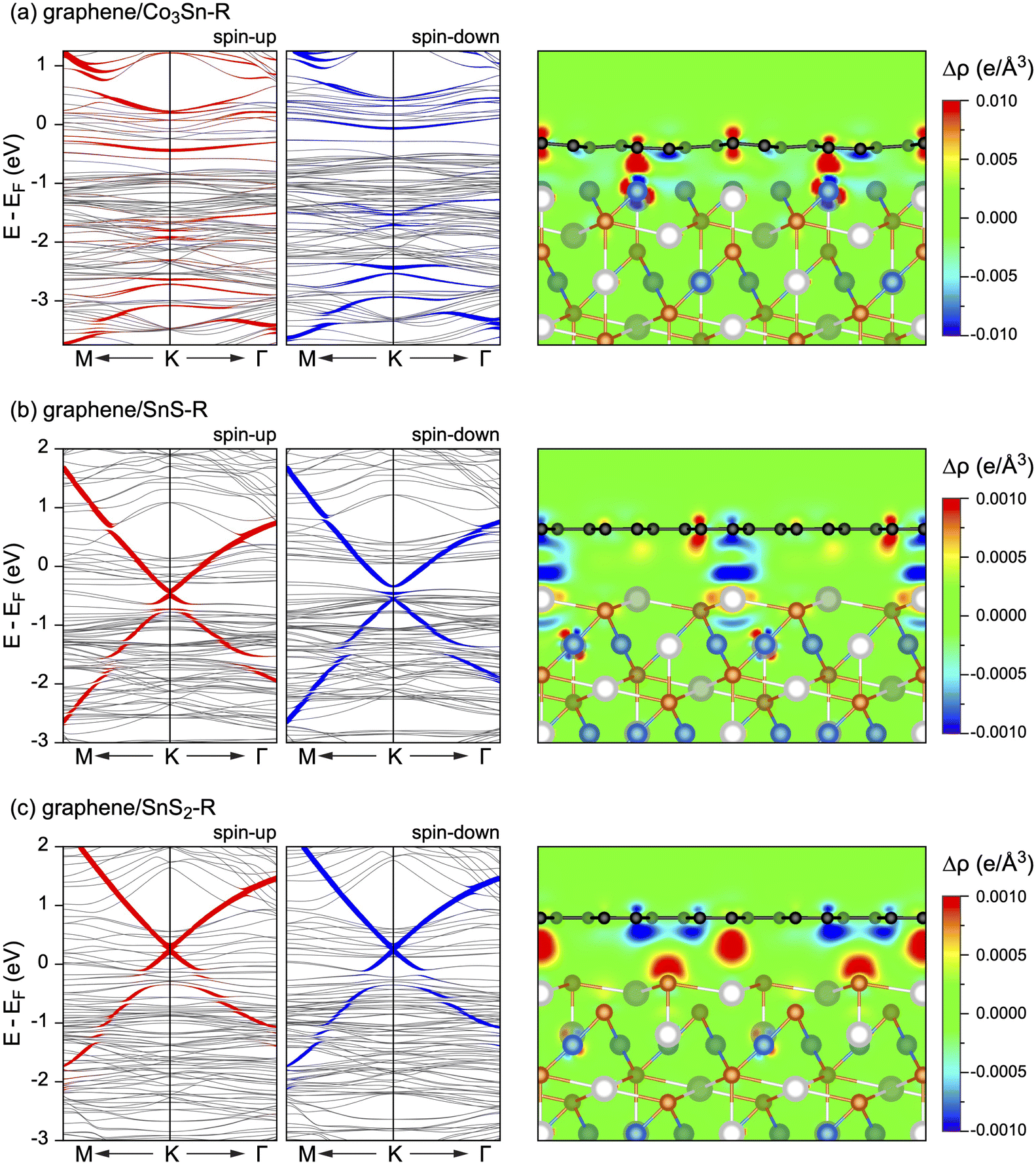 | ||
| Fig. 3 Band structures of graphene/Co3Sn2S2(001) in the vicinity of the K point of the graphene-derived Brillouin zone obtained for three different terminations of Co3Sn2S2: (a) graphene/Co3Sn-R; (b) graphene/SnS-R; (c) graphene/SnS3S2-R3Sn. The weight of the C-pz character is highlighted by the size of filled circles superimposed with the plot of the band structure. Side views for graphene/Co3Sn2S2(001) overlaid with electron charge difference maps: Δρ = ρAB − (ρA + ρB) with A: graphene and B: Co3Sn2S2(001). | ||
The interaction of graphene with the SnS- and SnS2-terminated Co3Sn2S2(001) is significantly weaker: the calculated Eint (Table 1) are typical for the weakly interacting graphene-based heterostructures. In both cases, the lowest-energy structures have C atoms located above the interface Sn atoms and S atoms of the lower sublayer (cf.Fig. 1j and m). Weak interaction of graphene with the substrate leads to minor changes in the structure of Co3Sn2S2 as compared to the pristine surface and the graphene layer remains flat. Yet, upon graphene adsorption, some charge redistribution is observed and atoms of the top two substrate layers are involved in this process. Interestingly, one can notice local charge transfer from graphene to the substrate, and also in the opposite direction (Fig. 3b and c). Overall, this interplay results in n-doped graphene in the case of SnS-terminated substrate (Fig. 3b) and p-doped graphene in the case of SnS2-terminated Co3Sn2S2(001) (Fig. 3c). This conclusion is also supported by Bader analysis Table 1).
In the case of the SnS-terminated Co3Sn2S2(001), the linear dispersion of the graphene-derived π-states is preserved and the position of a Dirac point (ED) of graphene is well below the Fermi energy, at EF − ED = −449 meV (Fig. 3b). The broken sublattice symmetry for carbon atoms of the graphene lattice and the effect of hybridisation between valence band states of graphene and underlying surface leads to the gap opening in the electronic spectrum of the graphene-derived π electrons directly at the Dirac point. Due to the vdW-type distance between graphene and substrate (d0 = 3.375 Å, see Table 1) and insignificant magnetic moment of Sn-atoms at the interface layer (mSn = −0.036μB), the magnetic moment of C-atoms keep their initial value unchanged (mC = −0.001μB). Consequently, the position of Dirac point is identical for both spin channels. Yet, the size of this gap is different for the spin-up and spin-down channels, as a consequence of the difference in the exchange splitting of states in the DOS of a substrate (see Fig. 2a and 3b and Table 1).
The effect of hybridisation between valence band states of graphene and underlying Co3Sn2S2(001) is also visible when considering the SnS2-terminated surface (Fig. 3c). However, due to the negligible magnetisation within the topmost substrate layers (Fig. 2d), the difference in the band gap width for the spin-up and spin-down channels is less pronounced. In this system graphene is p-doped and the position of Dirac point is at EF − ED = +255 meV.
We find an increase in MAE for all surface terminations studied after the graphene deposition (Table 1). At the same time, MAE calculated for the graphene/SnS–R interface is by 16% higher than the bulk value, which is important for spintronic and magnetoelectronic applications.
To make a reference to future experimental studies, the C 1s core-level shifts and C K near-edge X-ray absorption fine structure spectra (NEXAFS) were calculated for the considered graphene/Co3Sn2S2 interfaces.
The C 1s spectral line shape is known to be strongly affected by the interaction between graphene and substrate. The corresponding C 1s photoelectron spectrum of pristine graphene contains only one component. For the weakly interacting graphene/substrate interfaces, the C 1s line consists of only one component, which position is determined by the doping level of graphene. So, in the case of the quasi-free-standing graphene adsorbed on the SnS- and SnS2-terminated Co3Sn2S2(0001), the core-level shifts (CLS) calculated for the 4 nonequivalent carbon atoms in the graphene unit cell only slightly differ from each other, falling within the range of 10 meV and 80 meV, respectively (Fig. 4). At that, the calculated C 1s signals are shifted to more negative energies by 131 meV for graphene/SnS–R as compared to graphene/SnS2–R, corroborating the respective n-doping of a graphene layer in the former system. In the case of strongly interacting graphene/Co3Sn–R, the calculated CLS are within the range of 860 meV and the individual signals can be attributed to two groups separated by ca. 170 meV (Fig. 4): one of them is from atoms C1 and C3 (occupying the positions straight above the Co and Sn atoms of the topmost substrate layer (see Fig. 4, lower panel) located at lower relative energies and another peak at higher energies is composed of signals from C2 and C4. Overall, the C 1s spectrum is shifted by 264 meV to more negative relative energies for graphene/Co3Sn–R as compared to graphene/SnS2–R.
 | ||
| Fig. 4 (upper panel) C 1s core level shifts obtained for the energetically most stable configuration of graphene interfaced with Co3Sn2S2(001) (three surface terminations, see text for details). (lower panel) The crystallographic structures (with the highlighted interface layer and obscured deeper layers) used in the calculations. Inequivalent carbon atoms in the graphene layer are indicated. | ||
The method of NEXAFS spectroscopy is used to study the electronic structure of the unoccupied valence band states above EF and it is a complementary method to X-ray photoelectron spectroscopy and angle-resolved photoelectron spectroscopy used for the investigation of the energy distribution of the occupied states. Fig. 5 shows a series of the calculated C K-edge NEXAFS spectra for free-standing graphene, graphene/Co(001), and graphene/Co3Sn2S2(001) interfaces. In the considered NEXAFS spectra the core-level 1s electron of the carbon atom in a graphene layer is excited on the unoccupied valence band states above EF and being the atomic- and orbital-selective it allows getting information about the energy distribution of the π* and σ* states in a graphene layer. All NEXAFS spectra are presented in the relative photon energy scale with the position of the main peak for the C 1s → π* transition of a free-standing graphene at 0 eV.
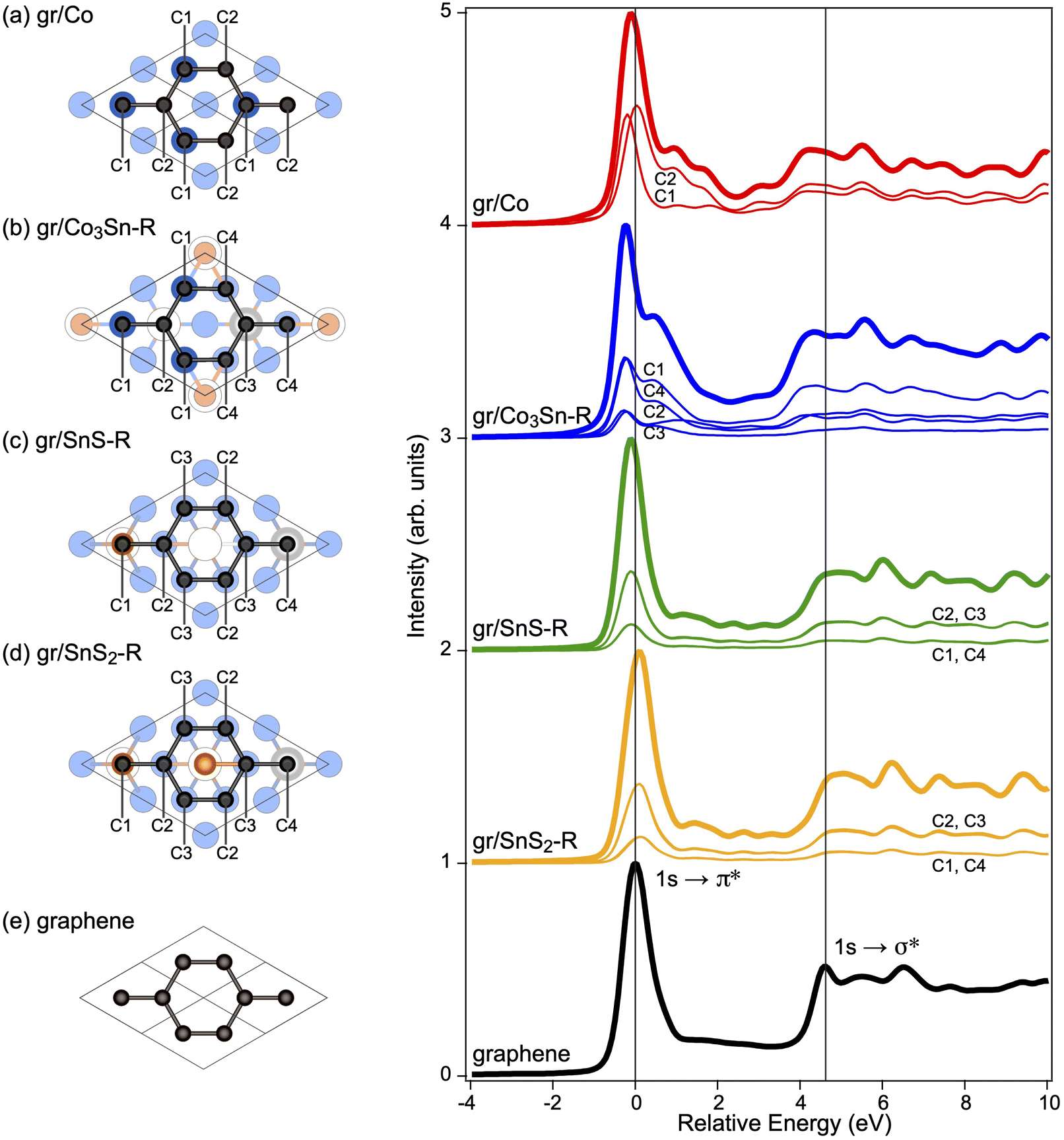 | ||
| Fig. 5 Calculated C K NEXAFS spectra for α = 40° for the freestanding graphene (e) and the energetically most stable configuration of graphene interfaced with Co(001) (a) and Co3Sn2S2(001) (b–d). The weighted spectra obtained for the individual atoms are shown with thin lines and the total spectrum is shown with thick line. The crystallographic structure (with the highlighted interface layer and obscured deeper layers) is shown at the left of each spectrum and inequivalent carbon atoms in the graphene layer are indicated. α is an angle between electric field vector of X-ray and the normal to the surface (see ref. 56). | ||
Let us first consider the reference spectra for the free-standing graphene and graphene/Co(001). The NEXAFS spectrum of free-standing graphene can be separated on two energy regions (see Fig. 5e): (i) 1s → π* contribution originating from transition of 1s core electron on C pz orbitals and (ii) 1s → σ* one originating from transition of 1s core electron on C sp2 hybrid orbitals. Fig. 5e shows the spectrum calculate for the graphene adopted the same lattice constant as in graphene/Co3Sn2S2(001). In this case, the region of −13 eV of the relative photon energy corresponds to the 1s → π* transitions and higher energy region above 4 eV corresponding to the 1s → σ* transitions. [Note: the energy splitting between the C 1s → π* and 1s → σ* transitions is reduced as compared to the pristine graphene in its equilibrium structure].
The structure of graphene/Co(001) widely accepted in the literature has the carbon atoms arranged in the so-called top-fcc configuration on Co(001): one carbon atom from the graphene unit cell (C1, see Fig. 5a) is placed above the Co interface atom and the second one (C2, see Fig. 5a) occupies the hollow fcc site of the Co(001) surface. As was mentioned already, this system belongs to the class of strongly interacting graphene–metal interfaces. Consequently, after graphene adsorption on Co(001) the C K NEXAFS spectrum (Fig. 5a) is strongly modified with respect to that of free-standing graphene. First, the position of the π* feature is shifted to lower energies as compared to the spectrum of free-standing graphene that is a result of strong n-doping (the downward shift of π* states for graphene/Co(001) compared to free-standing graphene). Then, in the region of the 1s → π* transition the graphene/Co(001) absorption spectra have a multiple-peak structure compared to those of graphene that is explained by the transitions of C 1s core electron into two unoccupied states (interface states), which are the result of hybridisation of the graphene π and Co 3d valence band states. These hybrid states have slightly different energy depending on the type of C-atom (C1 or C2) and on the spin-orientation. Finally, the visible reduction (by ca. 0.5 eV) in the energy separation between the π* and σ* features are observed for the graphene/Co(001) spectrum compared to that in the spectrum of free-standing graphene that is a result of strong interaction between graphene and a substrate, involving hybridisation between their valence band states. Thus, the reference spectra for the free-standing graphene and graphene/Co(001) are in reasonable agreement with previously calculated NEXAFS spectra for these objects (where available) as well as with the respective experimental data.19,20,61,62 The observed quantitative deviations are due to the stretched lattice constant of graphene.
When interacting with the SnS2-terminated Co3Sn2S2, graphene maintains its quasi free-standing nature. As a result, its absorption spectrum (Fig. 5d) looks very similar to that of free standing graphene. The most important difference is a shift of the whole spectrum to more positive energies that is the consequence of charge transfer from graphene to the substrate resulting in graphene p-doping. In the case of graphene/SnS–R, the opposite picture is observed: The absorption spectrum exhibiting the features of the free-standing graphene is shifted to the region of lower energies (Fig. 5c). This correlated with n-doping of graphene observed for this interface. The adsorption of graphene on the Co3Sn-terminated Co3Sn2S2 also leads to n-doping, which results in the shift of the 1s → π* peak to negative energies (Fig. 5b). At that, the interaction between graphene and a substrate in this case is significantly stronger than for two other terminations, that results in a double peak structure of the π* feature and reduction in the energy separation between the π* and σ* features, which is very similar to the results for the graphene/Co interface.
4. Conclusions
Relative stabilities of the pristine Co3Sn2S2 surfaces were studied by density functional theory. Among the three terminations of the (001) surface, SnS–R and SnS2–R were shown to be more stable than Co3Sn–R. This result is in a very good agreement with the experimental results,41 where most of the cleaved surfaces exhibit a triangular atomic structure characteristic for the Sn and the S atomic layers (Fig. 1d and e). Still, the formation of Co3Sn-termination, indicated by the characteristic kagome crystal structure (Fig. 1c), is also possible.41 The latter is confirmed by the calculated surface energy, which falls within the range of energies obtained for known stable surfaces (see e.g. ref. 63).Cleavage of the crystal reduces the coordination number of surface atoms, which leads to a change in the structure of the initially ideal surface. Consequently, this also leads to a modification in the electronic and magnetic properties of the formed system. In bulk Co3Sn2S2, the magnetic ordering arises from Co atoms, which form a kagome lattice network with one Sn atom located at the center. Disordering of this planar structure leads to the changes in the electronic and magnetic properties of the systems under study (Table 1). Thus, in the case of Co3Sn- and SnS2-terminated surfaces, the Co atoms relax in the depth of the layer, which contributes to the reduction of their magnetic moments. The DOS in the vicinity of the Fermi level is mainly composed of the 3d-state of Co (Fig. 2). As a result, Co3Sn–R becomes ferromagnetic, and in the case of SnS2–R the magnetic moment of Co located in the subsurface layer decreases so much that this surface almost completely loses its magnetic properties. Only SnS–R, where the relaxation effects are negligible, the HMF behaviour is preserved.
When graphene is deposited onto the Co3Sn2S2(001) surface, the C-atoms tend to occupy all possible positions above the surface Sn and Co (when available, see Fig. 1f, j and m) and the formation of a heterostructure is accompanied by changes in properties of the both counterparts. So, the interaction of graphene with the surface of Co3Sn2S2 results in the flattening of the Co3Sn layer and an increase in the Co magnetic moment, which in the case of SnS2–R still remains quite low (Table 1). When focusing on graphene, the result is intriguing. Although the behaviour of the graphene π states in the vicinity of the Fermi level are determined by the interplay of two factors – charge transfer from/onto graphene-derived π states and hybridisation of the electronic valence band states of graphene and Co3Sn2S2, the result is different for the three cases considered. In the case of graphene/Co3Sn–R, the n-doping of graphene leads to the positioning of ED within the Co-d band and several hybrid states are formed around the K point from the Co 3d states and graphene-derived π-states. As a result of this interaction, the linear dispersion of graphene π states in the vicinity of the Fermi level and the K point is completely destroyed (Fig. 3a). The absence of Co in the surface layer of SnS–R and SnS2–R makes the formation of 3d−π hybrid states impossible and the linear dispersion of the graphene-derived π-states remains intact. Nevertheless, the hybridisation of the valence band states of graphene and Co3Sn2S2 far away from the Dirac point leads to the opening of a sizeable band gap exactly at the Dirac point, which is located below EF in the case of graphene/SnS–R (Fig. 3b) and above EF in the case of graphene/SnS2–R (Fig. 3c). Thus, the formation of the graphene–Co3Sn2S2 heterostructures allows one to get a virtually full spectrum of systems – strongly bonded graphene, weakly bonded graphene with p- or n-doping, and also detect the formation of a gap exactly at ED. All these features of the interaction of graphene with Co3Sn2S2 are reflected in the calculated C 1s core-level shifts (Fig. 4) and C K NEXAFS spectra (Fig. 5), which can be directly compared with available experimental results.
A final note relates to the magnetic anisotropy energy, which is of crucial importance from the fundamental or technological point of views since it provides an energy scale for the stability of magnetic domains, where for example magnetic information is stored. As mentioned above, bulk Co3Sn2S2 is known for its stable perpendicular magnetic anisotropy. The reduced symmetry of surface atoms as compared to bulk atoms gives rise to reduction of a magnetic anisotropy with respect to the bulk value (Table 1). Yet, the easy axis keeps its direction for all Co3Sn2S2-terminations under study. Deposition of graphene, which can protect the underlying material from the environment, enhances the perpendicular magnetic anisotropy for all heterostructures under study (Table 1). At that, the MAE calculated for graphene/SnS–R is by 16% higher than the bulk value. Keeping in mind that SnS–R can be easily obtained by cleavage of the bulk Co3Sn2S2, this new interface shows promise for development as a stable magnetic recording media.
Data availability
Data obtained during this study are available from the corresponding authors on reasonable request.Conflicts of interest
There are no conflicts to declare.Acknowledgements
The authors gratefully acknowledge the computing time granted by the Resource Allocation Board and provided on the supercomputer Lise at NHR@ZIB as part of the NHR infrastructure. The calculations for this research were conducted using computing resources under the project bec00256. Y. D. acknowledges support by the project Centre for Advanced Laser Techniques (CALT), co-funded by the European Union through the European Regional Development Fund under the Competitiveness and Cohesion Operational Programme (Grant No. KK.01.1.1.05.0001). The authors thank the National Natural Science Foundation of China (Grant No. 22272104) for financial support.Notes and references
- J. Liu and T. Hesjedal, Adv. Mater., 2023, 35, e2102427 CrossRef PubMed.
- M. Gibertini, M. Koperski, A. F. Morpurgo and K. S. Novoselov, Nat. Nanotechnol., 2019, 14, 408–419 CrossRef PubMed.
- X. Li, S. Aftab, A. Abbas, S. Hussain, M. Aslam, F. Kabir, H. S. Abd-Rabboh, H. Hegazy, F. Xu and M. Z. Ansari, Nano Energy, 2023, 118, 108979 CrossRef.
- S. Wang, W. Liao, H. Su, S. Pang, C. Yang, Y. Fu and Y. Zhang, Energy Fuels, 2023, 37, 1633–1656 CrossRef.
- X. Zhang, Mater. Res. Lett., 2020, 8, 49–59 CrossRef.
- Y. Zhu, K. Ameyama, P. M. Anderson, I. J. Beyerlein, H. Gao, H. S. Kim, E. Lavernia, S. Mathaudhu, H. Mughrabi, R. O. Ritchie, N. Tsuji, X. Zhang and X. Wu, Mater. Res. Lett., 2021, 9, 1–31 CrossRef.
- H. Zheng, Y. Li, H. Liu, X. Yin and Y. Li, Chem. Soc. Rev., 2011, 40, 4506–4524 RSC.
- Y. Li, J. Zhang, Q. Chen, X. Xia and M. Chen, Adv. Mater., 2021, 33, e2100855 CrossRef.
- Z. Wu, W. Jie, Z. Yang and J. Hao, Mater. Today Nano, 2020, 12, 100092 CrossRef.
- W. Wu, S. Luo, Y. Huang, H. He, P. K. Shen and J. Zhu, Mater. Chem. Front., 2023, 8, 1064–1083 RSC.
- Y. Liu, N. O. Weiss, X. Duan, H.-C. Cheng, Y. Huang and X. Duan, Nat. Rev. Mater., 2016, 1, 16042 CrossRef.
- S. Zhang, J. Liu, M. M. Kirchner, H. Wang, Y. Ren and W. Lei, J. Phys. D: Appl. Phys., 2021, 54, 433001 CrossRef.
- Z. Wang, B. Xu, S. Pei, J. Zhu, T. Wen, C. Jiao, J. Li, M. Zhang and J. Xia, Sci. China Inf. Sci., 2022, 65, 211401 CrossRef.
- P. V. Pham, S. C. Bodepudi, K. Shehzad, Y. Liu, Y. Xu, B. Yu and X. Duan, Chem. Rev., 2022, 122, 6514–6613 CrossRef CAS.
- A. H. C. Neto, F. Guinea, N. M. R. Peres, K. S. Novoselov and A. K. Geim, Rev. Mod. Phys., 2009, 81, 109–162 CrossRef.
- W. Han, R. K. Kawakami, M. Gmitra and J. Fabian, Nat. Nanotechnol., 2014, 9, 794–807 CrossRef CAS.
- A. K. Sood, I. Lund, Y. R. Puri, H. Efstathiadis, P. Haldar, N. K. Dhar, J. Lewis, M. Dubey, E. Zakar, P. Wijewarnasuriya, D. L. Polla and M. Fritze, Graphene – New Trends and Developments, InTechOpen, 2015 Search PubMed.
- Y. S. Dedkov, M. Fonin and C. Laubschat, Appl. Phys. Lett., 2008, 92, 052506 CrossRef.
- M. Weser, Y. Rehder, K. Horn, M. Sicot, M. Fonin, A. B. Preobrajenski, E. N. Voloshina, E. Goering and Y. S. Dedkov, Appl. Phys. Lett., 2010, 96, 012504 CrossRef.
- Y. S. Dedkov and M. Fonin, New J. Phys., 2010, 12, 125004 CrossRef CAS.
- Y. Matsumoto, S. Entani, A. Koide, M. Ohtomo, P. V. Avramov, H. Naramoto, K. Amemiya, T. Fujikawa and S. Sakai, J. Mater. Chem. C, 2013, 1, 5533–5537 RSC.
- D. Usachov, A. Fedorov, M. M. Otrokov, A. Chikina, O. Vilkov, A. Petukhov, A. G. Rybkin, Y. M. Koroteev, E. V. Chulkov, V. K. Adamchuk, A. Grüneis, C. Laubschat and D. V. Vyalikh, Nano Lett., 2015, 15, 2396–2401 CrossRef CAS PubMed.
- D. Marchenko, A. Varykhalov, J. Sánchez-Barriga, O. Rader, C. Carbone and G. Bihlmayer, Phys. Rev. B: Condens. Matter Mater. Phys., 2015, 91, 235431 CrossRef.
- W. Yue, Q. Guo, Y. Dedkov and E. Voloshina, ACS Omega, 2022, 7, 7304–7310 CrossRef CAS PubMed.
- V. M. Karpan, P. A. Khomyakov, A. A. Starikov, G. Giovannetti, M. Zwierzycki, M. Talanana, G. Brocks, J. V. D. Brink and P. J. Kelly, Phys. Rev. B: Condens. Matter Mater. Phys., 2008, 78, 195419 CrossRef.
- E. Voloshina and Y. Dedkov, Phys. Chem. Chem. Phys., 2012, 14, 13502–13514 RSC.
- E. N. Voloshina and Y. S. Dedkov, Mater. Res. Express, 2014, 1, 035603 CrossRef CAS.
- E. N. Voloshina, A. Generalov, M. Weser, S. Böttcher, K. Horn and Y. S. Dedkov, New J. Phys., 2011, 13, 113028 CrossRef.
- Y. Dedkov, W. Klesse, A. Becker, F. Späth, C. Papp and E. Voloshina, Carbon, 2017, 121, 10–16 CrossRef.
- E. Voloshina and Y. Dedkov, J. Phys. Chem. Lett., 2019, 10, 3212–3216 CrossRef.
- Y. Dedkov, J. Yang, H. Hu, Y. Jin, M. Yan, Y. Jin, J. Zhou and E. Voloshina, ACS Appl. Mater. Interfaces, 2023, 15, 26190–26198 CrossRef.
- R. Xiao, D. Fritsch, M. D. Kuzmin, K. Koepernik, H. Eschrig, M. Richter, K. Vietze and G. Seifert, Phys. Rev. Lett., 2009, 103, 187201 CrossRef PubMed.
- N. Rougemaille, A. T. N'Diaye, J. Coraux, C. Vo-Van, O. Fruchart and A. K. Schmid, Appl. Phys. Lett., 2012, 101, 142403 CrossRef.
- R. Decker, J. Brede, N. Atodiresei, V. Caciuc, S. Blügel and R. Wiesendanger, Phys. Rev. B: Condens. Matter Mater. Phys., 2013, 87, 041403 CrossRef.
- A. D. Vu, J. Coraux, G. Chen, A. T. NDiaye, A. K. Schmid and N. Rougemaille, Sci. Rep., 2016, 6, 24783 CrossRef.
- H. Yang, A. D. Vu, A. Hallal, N. Rougemaille, J. Coraux, G. Chen, A. K. Schmid and M. Chshiev, Nano Lett., 2016, 16, 145–151 CrossRef PubMed.
- R. Weihrich, I. Anusca and M. Zabel, Z. Anorg. Allg. Chem., 2004, 630, 1767 Search PubMed.
- W. Schnelle, A. Leithe-Jasper, H. Rosner, F. M. Schappacher, R. Pöttgen, F. Pielnhofer and R. Weihrich, Phys. Rev. B: Condens. Matter Mater. Phys., 2013, 88, 144404 Search PubMed.
- M. Yan, Y. Jin, X. Hou, Y. Guo, A. Tsaturyan, A. Makarova, D. Smirnov, Y. Dedkov and E. Voloshina, J. Phys. Chem. Lett., 2021, 12, 9807–9811 Search PubMed.
- L. Jiao, Q. Xu, Y. Cheon, Y. Sun, C. Felser, E. Liu and S. Wirth, Phys. Rev. B, 2019, 99, 245158 Search PubMed.
- N. Morali, R. Batabyal, P. K. Nag, E. Liu, Q. Xu, Y. Sun, B. Yan, C. Felser, N. Avraham and H. Beidenkopf, Science, 2019, 365, 1286–1291 Search PubMed.
- G. Li, Q. Xu, W. Shi, C. Fu, L. Jiao, M. E. Kamminga, M. Yu, H. Tüysüz, N. Kumar, V. Süß, R. Saha, A. K. Srivastava, S. Wirth, G. Auffermann, J. Gooth, S. Parkin, Y. Sun, E. Liu and C. Felser, Sci. Adv., 2019, 5, eaaw9867 CrossRef.
- G. Kresse and J. Furthmüller, Phys. Rev. B: Condens. Matter Mater. Phys., 1996, 54, 11169–11186 CrossRef.
- G. Kresse and D. Joubert, Phys. Rev. B: Condens. Matter Mater. Phys., 1999, 59, 1758–1775 CrossRef.
- J. P. Perdew, K. Burke and M. Ernzerhof, Phys. Rev. Lett., 1996, 77, 3865–3868 CrossRef CAS PubMed.
- P. E. Blöchl, Phys. Rev. B: Condens. Matter Mater. Phys., 1994, 50, 17953–17979 CrossRef.
- P. E. Blöchl, O. Jepsen and O. K. Andersen, Phys. Rev. B: Condens. Matter Mater. Phys., 1994, 49, 16223–16233 CrossRef PubMed.
- S. Grimme, J. Antony, S. Ehrlich and H. Krieg, J. Chem. Phys., 2010, 132, 154104 CrossRef PubMed.
- K. Reuter and M. Scheffler, Phys. Rev. B: Condens. Matter Mater. Phys., 2001, 65, 035406 CrossRef.
- E. Sanville, S. D. Kenny, R. Smith and G. NHenkelman, J. Comput. Chem., 2007, 28, 899–908 CrossRef CAS.
- W. Tang, E. Sanville and G. Henkelman, J. Phys.: Condens. Matter, 2009, 21, 084204 CrossRef CAS.
- G. Henkelman, A. Arnaldsson and H. Jónsson, Comput. Mater. Sci., 2006, 36, 354–360 CrossRef.
- E. Miniussi, M. Pozzo, A. Baraldi, E. Vesselli, R. R. Zhan, G. Comelli, T. O. MenteÅŸ, M. A. Niño, A. Locatelli, S. Lizzit and D. Alfè, Phys. Rev. Lett., 2011, 106, 216101 CrossRef CAS PubMed.
- ELSA software, https://condmat.prof/elsa (accessed: November 2024) Search PubMed.
- R. E. Ovcharenko, I. I. Tupitsyn, E. P. Savinov, E. N. Voloshina, B. Paulus, Y. S. Dedkov and A. S. Shulakov, Phys. Chem. Chem. Phys., 2013, 15, 6749–6756 RSC.
- E. Voloshina, R. Ovcharenko, A. Shulakov and Y. Dedkov, J. Chem. Phys., 2013, 138, 154706 CrossRef PubMed.
- Y. S. Dedkov, M. Holder, S. L. Molodtsov and H. Rosner, J. Phys. Conf. Ser., 2008, 100, 072011 CrossRef.
- M. Holder, Y. S. Dedkov, A. Kade, H. Rosner, W. Schnelle, A. Leithe-Jasper, R. Weihrich and S. L. Molodtsov, Phys. Rev. B: Condens. Matter Mater. Phys., 2009, 79, 205116 CrossRef.
- M. P. Ghimire, J. I. Facio, J.-S. You, L. Ye, J. G. Checkelsky, S. Fang, E. Kaxiras, M. Richter and J. V. D. Brink, Phys. Rev. Res., 2019, 1, 032044 CrossRef CAS.
- K. Wang, T. Vincent, J. B. Bouhiron, S. Pons, D. Roditchev, S. Simon, M. Fonin, B. Paulus, Y. Dedkov, S. Vlaic and E. Voloshina, Carbon, 2021, 183, 251–258 CrossRef CAS.
- O. Vilkov, A. Fedorov, D. Usachov, L. V. Yashina, A. V. Generalov, K. Borygina, N. I. Verbitskiy, A. Grüneis and D. V. Vyalikh, Sci. Rep., 2013, 3, 2168 CrossRef CAS.
- V. O. Shevelev, K. A. Bokai, A. A. Makarova, D. Marchenko, O. Y. Vilkov, V. Y. Mikhailovskii, D. V. Vyalikh and D. Y. Usachov, J. Phys. Chem. C, 2020, 124, 17103–17110 CrossRef CAS.
- X. Li and J. Paier, J. Phys. Chem. C, 2016, 120, 1056–1065 CrossRef CAS.
| This journal is © The Royal Society of Chemistry 2025 |