
 Open Access Article
 This Open Access Article is licensed under a
 Creative Commons Attribution 3.0 Unported Licence
Post-transition metal Sn-based chalcogenide perovskites: a promising lead-free and transition metal alternative for stable, high-performance photovoltaics†
Surajit
Adhikari
 *,
Sankhasuvra
Das
and
Priya
Johari
*
*,
Sankhasuvra
Das
and
Priya
Johari
*
Department of Physics, School of Natural Sciences, Shiv Nadar Institution of Eminence, Greater Noida, Gautam Buddha Nagar, Uttar Pradesh 201314, India. E-mail: sa731@snu.edu.in; priya.johari@snu.edu.in
First published on 28th February 2025
Abstract
Chalcogenide perovskites (CPs) have emerged as promising materials for optoelectronic applications due to their stability, non-toxicity, small bandgaps, high absorption coefficients, and defect tolerance. Although transition metal-based CPs, particularly those incorporating Zr and Hf, have been well-studied, they often exhibit higher bandgaps, lower charge carrier mobility, and reduced efficiency compared to lead-based halide perovskites (HPs). Tin (Sn), a post-transition metal with a similar oxidation state (+4) to Zr and Hf in ABX3 structures but with different valence characteristics, remains underexplored in CPs. Given the influence of valence states on material properties, Sn-based CPs are of great interest. This study employs density functional theory (DFT), density functional perturbation theory (DFPT), and many-body perturbation theory (GW and BSE) to investigate a series of distorted Sn-based CPs (ASnX3, A = Ca, Sr, Ba; X = S, Se). Our results demonstrate that these perovskites are mechanically stable and exhibit lower direct G0W0 bandgaps (0.79–1.50 eV) compared to their Zr- and Hf-based counterparts. Analysis of carrier-phonon interactions reveals that the charge-separated polaronic state is less stable than the bound exciton state in these materials. Additionally, polaron-assisted charge carrier mobilities for electrons (21.33–416.02 cm2 V−1 s−1) and holes (7.02–260.69 cm2 V−1 s−1) are comparable to or higher than those in lead-based HPs and significantly exceed those of Zr- and Hf-based CPs, owing to reduced carrier-phonon coupling. The estimated spectroscopic limited maximum efficiency (24.2–31.2%)—confirmed through perovskite solar cell (PSC) simulations using SCAPS-1D software—indicates that these materials are promising candidates for photovoltaic applications. Overall, this study highlights the potential of Sn as a superior alternative to transition metals in CPs, particularly for photovoltaic applications, where smaller electronegativity differences lead to reduced bandgaps and reduced polaronic effects improved charge carrier mobility. These findings are expected to stimulate further experimental investigation into Sn-based CPs.
1 Introduction
Chalcogenide perovskites (CPs)1–4 have recently emerged as a potential alternative for the high-performing inorganic–organic halide perovskites (IOHPs).5–8 While IOHPs face significant obstacles for their large-scale industrial applications owing to the toxicity of lead and instability due to the presence of organic cations,9,10 CPs show promise because of their vast availability in the earth's crust, non-toxic nature, and exceptional stability.1,11–13 In addition to these advantages, CPs exhibit favorable characteristics such as small electronic bandgap, high absorption coefficient, promising defect tolerance, good charge carrier mobility, and excellent power conversion efficiency (PCE),2–4,14,15 which point toward their potential application in a variety of optoelectronic devices.Similar to the typical three-dimensional halide perovskites (HPs), the chemical formula of chalcogenide perovskites is expressed as ABX3,4,16 where A and B stand for divalent alkali-earth metal cations (Ca2+, Sr2+, Ba2+) and tetravalent transition metal cations (Ti4+, Zr4+, and Hf4+), respectively, and X is typically a chalcogen anion such as S2− or Se2−. Numerous experimental and theoretical investigations have demonstrated the successful synthesis of chalcogenide perovskites and unveiled their intriguing properties.1–4,11–14,17,18 For example, Lelieveld et al.17 synthesized the distorted phase of CaZrS3, SrZrS3, BaZrS3, CaHfS3, SrHfS3, and BaHfS3 in 1980, while later, the needle-like phases18–20 of SrZrS3, SrZrSe3, and SrHfSe3 CPs were also synthesized by various groups at the end of 20th century and beginning of the 21st century. In 2016, Perera et al.21 used high-temperature sulfurization of the oxides with CS2 to synthesize AZrS3 (A = Ba, Ca, and Sr). On the other hand, in 2015, Sun et al.4 theoretically affirmed the formation of two distinct phases of CPs at room temperature: the needle-like phase (NH4CdCl3-type) and the distorted phase (GdFeO3-type), both sharing the orthorhombic structure with the same space group Pnma (no. 62), and predicted them to be promising for application in solar cells. In addition, several first-principles DFT-based studies have been conducted, indicating that CPs exhibit interesting electronic and optical properties suitable for use in photovoltaic applications.4,14–16,22
Several studies have primarily focused on Zr ([Kr]4d2 5s2) and Hf ([Xe]4f14 5d2 6s2) transition metal-based CPs, where the valence band configurations involve d- and s-orbitals.14,15,22 These materials are demonstrated to exhibit exciton binding energies ranging from 0.02 to 0.26 eV, which are comparable to or higher than those observed in conventional lead-based HPs (0.01–0.10 eV).23–25 However, the main drawback of these CPs lies in their reduced charge carrier mobility (6.84–77.59 cm2 V−1 s−1) and lower PCE (10.56–25.02%) compared to conventional HPs, which have charge carrier mobility and PCE in the range of 57–290 cm2 V−1 s−1 (ref. 26 and 27) and 21.15–28.97%,28,29 respectively. These limitations are majorly due to prominent polaronic effects and relatively higher bandgaps, which hinder their effectiveness for solar cell applications. This makes the exploration of alternatives for the B-site cation even more crucial in order to achieve high polaronic charge carrier mobility along with high PCE, thereby enhancing the effectiveness of CPs for solar cell applications.
The polaronic effects are more pronounced in transition metal-based CPs. However, if the post-transition metal Sn ([Kr]4d10 5s2 5p2), which also exhibits a +4 oxidation state, is used in place of transition metals like Zr and Hf, the polaronic effects could be mitigated due to different valence states. Additionally, a lower difference in the electronegativity of Sn and X (S, Se) may offer the potential for achieving appropriate bandgaps for photovoltaic applications. Recent first-principles calculations highlight the potential of Sn as a B-site cation via distorted SrSnX3 (X = S, Se) perovskites as promising photovoltaic materials solely based on their electronic and optical properties up to the HSE06 level.30,31 Experimental investigations have substantiated this potential by fabricating distorted CaSnS3 perovskite at 500 °C.32 Basera et al.14 have furthermore provided valuable insights into the photovoltaic properties of distorted CaSnS3, as well as needle-like phases of BaSnS3 and SrSnS3 perovskites. However, the challenge posed by these needle-like CPs lies in their higher bandgap (1.91–2.04 eV) and lower theoretical efficiency (21.80%). In contrast, the bandgap of distorted CaSnS3 falls within the optimal range at 1.43 eV, with theoretical efficiency reaching up to 32.45%.14 Motivated by these findings, we aim to conduct a comprehensive theoretical analysis of post-transition metal Sn-based distorted CPs to elucidate their suitable photovoltaic application features.
Henceforth, we have endeavored to meticulously explore the optoelectronic, transport, excitonic, and polaronic properties of distorted Sn-based, ASnX3 (A = Ca, Sr, Ba; X = S, Se) CPs utilizing a combination of density functional theory (DFT),33,34 density functional perturbation theory (DFPT),35 and advanced many-body perturbation theory based methodologies like GW and BSE.36,37 Initially, the crystal structures are optimized using the semilocal PBE38 exchange–correlation (xc) functional, and their stability has been examined. The electronic properties of the relaxed structures are calculated using the HSE0639 xc functional as well as G0W0@PBE40,41 methodology. The investigated CPs exhibit direct bandgaps ranging from 0.79 to 1.50 eV, which fall within a similar range to that of conventional lead-based HPs23,28 and are lower than the bandgaps observed in Zr- and Hf-based CPs.14,15,22 Following this, optical properties and exciton binding energies (EB) are determined through the Bethe–Salpeter equation (BSE)42,43 method. Furthermore, employing the DFPT technique, the ionic contribution to the dielectric function is computed, and the Fröhlich model is invoked to evaluate polaronic attributes such as carrier-phonon coupling strength and polaron mobility (21.33–416.02 cm2 V−1 s−1). Conclusively, the estimation of the spectroscopic limited maximum efficiency (SLME)44 between 24.20–31.20% utilizing the quasiparticle (QP) bandgap and absorption coefficient underscores ASnX3 as a material with significant potential for photovoltaic applications. This has been further confirmed by performing the conventional device (FTO/TiO2/ASnX3/spiro-OMeTAD/Au) simulations using SCAPS-1D software.45–48
2 Computational methodologies and numerical simulations
2.1 Computational details
In this work, state-of-the-art first-principles calculations based on density functional theory (DFT),33,34 density functional perturbation theory (DFPT),35 and many-body perturbation theory (MBPT)36,37 were performed using the Vienna ab initio simulation package (VASP).49,50 In all constituent elements, the valence electrons and atomic core interactions were described using the projector-augmented wave (PAW) pseudopotentials.51 The PAW pseudopotentials with valence-electron configurations considered for Ca, Sr, Ba, Sn, S, and Se were 3s2 3p6 4s2, 4s2 4p6 5s2, 5s2 5p6 6s2, 4d10 5s2 5p2, 3s2 3p4, and 4s2 4p4, respectively. For the structural optimization, the generalized gradient approximation (GGA)38 based exchange–correlation (xc) functional of Perdew, Burke, and Ernzerhof (PBE) was employed, which takes into account the electron–electron interactions. The plane-wave cutoff energy was set to 400 eV, and the electronic self-consistent-field iteration energy convergence threshold was chosen as 10−6 eV. The lattice constants and coordinates of all the atoms were fully optimized until the Helmann–Feynman forces on each atom were less than 0.01 eV Å−1. The Γ-centered 7 × 7 × 5 k-point sampling was used for Brillouin zone integration in order to determine the optimized structures. The Visualization for Electronic and STructural Analysis (VESTA)52 software package was used to display the optimized crystal structures.The phonon spectra were calculated using the DFPT method as implemented in the PHONOPY53 package by considering a 2 × 2 × 2 supercell. Since, GGA is known to underestimate the bandgap, the electronic band structures were computed using the hybrid HSE0639 xc functional as well as the many-body perturbation theory (MBPT) based GW40,41 (G0W0@PBE) method. Note that the spin–orbit coupling (SOC) effect was not considered as it does not impact the bandgap (for details, see the ESI†) of the considered systems. The effective mass was computed by SUMO54 using a parabolic fitting of the band edges. We also carried out Bethe–Salpeter equation (BSE)42,43 based calculations on top of the single-shot GW(G0W0)@PBE to precisely estimate the optical properties, which takes explicitly into account the electron–hole interaction. Here, a Γ-centered 3 × 3 × 2 k-grid and 640 converged NBANDS were used for the GW–BSE calculations. The polarizability calculations were performed using a frequency grid of 60 points to ensure accurate results. In our GW calculations, we used the plasmon-pole approximation (PPA) to model the frequency dependence of the dielectric function (ALGO = GW0). Additionally, the plane-wave cutoff for the response function was set to ENCUTGW = 267 eV (2/3 of ENCUT) for both GW and BSE calculations. The electron–hole kernel for the BSE calculations was generated by considering 24 occupied and 24 unoccupied bands. The VASPKIT55 package was used to post-process the elastic and optical properties. The ionic contribution to the dielectric constant was also calculated using the DFPT method.
Using the hydrogenic Wannier–Mott (WM)22,56 model, the exciton binding energy (EB) for a screened Coulomb interacting e−h pair is calculated as follows:
 | (1) |
The phonon screening correction to the exciton binding energy (EB) is given by ref. 57:
 | (2) |
Within the framework of Fröhlich's polaron model, the longitudinal optical phonons and the electron traveling through the lattice interact via the dimensionless Fröhlich parameter α, which is expressed as,59
 | (3) |
| Ep = (−α − 0.0123α2)ħωLO | (4) |
Feynman's extended version of Fröhlich's polaron theory (for a small α) is also used to obtain the effective mass of the polaron (mp) as follows:60
 | (5) |
Finally, using the Hellwarth polaron model,58 the polaron mobility is defined as follows:
 | (6) |
2.2 SCAPS-1D numerical simulations
SCAPS-1D software is utilized to conduct numerical device simulations on solar cells to assess their performance and aid in design optimization. The tool was developed by Prof. M. Burgelman at the Department of Electronics and Information Systems (ELIS) of the University of Gent, Belgium.61,62 SCAPS solves Poisson's equation, which correlates the electrostatic potential to the overall charge density, along with continuity equations for electrons and holes in the conduction and valence bands, respectively. It can predict device characteristics such as current density–voltage curves, efficiency, energy bands, and other properties of the solar cell structure under illumination. Fig. 5(a) shows the proposed perovskite solar cell (PSC) structure having the architecture of FTO/TiO2/perovskite/spiro-OMeTAD/Au. In this proposed structure, spiro-OMeTAD was used as the hole transport layer (HTL), TiO2 was used as the electron transport layer (ETL), FTO (fluorine-doped tin oxide) as the transparent conducting oxide (TCO), and perovskite as the absorber layer. Gold (Au), having a work function of 5.1 eV, was employed as the back metallic contact. The simulation parameters for the HTL, ETL, and FTO, chosen based on theoretical and experimental results,45 are listed in Table S15 of the ESI.† Table S16 (ESI†) also shows the input parameters for the perovskite layer, estimated through our theoretical calculations (for details, see the ESI†). The simulations were conducted under the illumination of AM 1.5G at 300 K working temperature. The Poisson's equation and the continuity equations of both the carriers (electrons and holes) for SCAPS-1D simulation are written as,46,47 | (7) |
 | (8) |
 | (9) |
Here ψ is the electrostatic potential, ε is the permittivity of the material, p and n are electron and hole concentrations, ND and NA are donor and acceptor densities, Jn and Jp are electron and hole current densities, ρn and ρp are electron and hole distribution, R is the recombination, and Gop is the optical generation rate.
The open circuit voltage (Voc) of the perovskite solar cell (PSC) is given by ref. 45,
 | (10) |
 | (11) |
 | (12) |
3 Results and discussion
In this study, we undertook a systematic and thorough investigation into the distorted phases of post-transition metal Sn-based chalcogenide perovskites ASnX3 (A = Ca, Sr, Ba; X = S, Se) to explore their potential optoelectronic features. The subsequent sections delve into the stability as well as the structural, electronic properties, transport phenomena, optical properties, excitonic dynamics, polaronic effects, and spectroscopic limited maximum efficiency (SLME) of ASnX3 chalcogenide perovskites. This detailed examination and discussion aims to establish a foundational understanding and provide insights to guide future experimental endeavors.3.1 Structural properties
The orthorhombic distorted crystal structure with the space group Pnma (no. 62)17 of chalcogenide perovskites ASnX3 (A = Ca, Sr, Ba; X = S, Se) are presented in Fig. 1(a) and Fig. S1 (ESI†). The crystal structure of these compounds usually consists of four formula units, i.e., 20 atoms, of which 4 are Ca/Sr/Ba, 4 are Sn, and 12 are S or Se atoms. In this distorted phase, the alkaline earth elements (A-site cations) have 12-fold coordination, and they form cuboctahedrons with chalcogenides X (S or Se). On the other hand, the corner-sharing distorted octahedrons [SnX6]8− are produced due to the 6-fold coordination of the Sn cation with X (S or Se) atoms in a distorted and tilted way. The lattice parameters of the optimized crystal structures are calculated using the PBE xc functional and are tabulated in Table 1. It is found that the lattice parameters are in good agreement with previous theoretical and available experimental results.30,32 However, for CaSnS3, there is a discrepancy in the c-lattice constant between the theoretical and experimental values, which could influence the bandgap, as variations in bond lengths and angles modify the electronic band dispersion. In addition, Table S1 (ESI†) presents detailed information on the octahedral distortions of SnX6 octahedra in ASnX3 (A = Ca, Sr, Ba; X = S, Se) CPs, including parameters such as average bond length, bond angle variance, polyhedral volume, and distortion index. The results indicate that the SnX6 octahedra in BaSnX3 (X = S, Se) undergo greater lattice distortion than those in other compounds, likely due to the larger ionic radius of Ba2+, which influences the local bonding environment around the octahedra.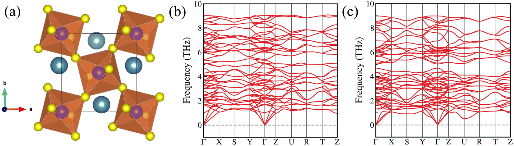 | ||
| Fig. 1 (a) Crystal structure of CaSnS3 in the orthorhombic distorted phase, and phonon dispersion curves of (b) SrSnS3, and (c) BaSnS3 calculated using the DFPT method. Blue, purple, and yellow balls represent Ca, Sn, and S atoms, respectively. | ||
The crystallographic stability of these CPs is quantitatively identified by calculating the Goldschmidt tolerance factor (t), the octahedral factor (μ), and the new tolerance factor (τ)56,63,64 (for details, see the ESI†). From Table S2 (ESI†), it can be noticed that the t, μ, and τ values of these investigated CPs are in the range of 0.879–0.964, 0.348–0.375, and 4.174–4.721, respectively, confirming the reasonable structural stability of these distorted CPs.16,63 Furthermore, the decomposition energy is also calculated for these materials using the PBE xc functional to ascertain their thermodynamic stability (for details, see Table S3 of the ESI†). The negative decomposition energy reveals these perovskites to be unstable at 0 K. Still, there remains a possibility for them to stabilize at higher temperatures, as also demonstrated by Hamza et al. by synthesizing CaSnS3 perovskite at 500 °C,32 which is an indicator of their higher temperature stability. Furthermore, the dynamical and mechanical stability of the studied CPs are examined.
In Fig. 1(b) and (c), the phonon spectra of SrSnS3 and BaSnS3 CPs have been depicted, which validates their dynamical stability at 0 K. The rest of the compounds are found to be unstable at 0 K, but they may become dynamically stable at higher temperatures, as discussed before. To investigate the mechanical stability, the second-order elastic coefficients (Cij) of these CPs are calculated using the energy-strain approach65 (for details, see the ESI†). The computed Cij values of these compounds are listed in Table S4 (ESI†), and they are found to satisfy the Born stability criteria.65 Using these elastic coefficients, the bulk modulus (B), shear modulus (G), Young's modulus (Y), and Poisson's ratio (ν) of these materials66,67 are investigated (for details, see the ESI†). The fragility of the materials is studied in terms of Pugh's suggested ratio (B/G)68 and Poisson's ratio (ν). The calculated values of B/G (>1.75) and ν (>0.26) reveal that the examined CPs are ductile in nature (see Table S4, ESI†). Additionally, the longitudinal (vl), transverse (vt), and average (vm) elastic wave velocities and the Debye temperature (ΘD)69 are calculated (see Table S5, ESI†), as they hold crucial significance for flexible optoelectronic applications.
3.2 Electronic properties
After examining the stability, the electronic properties, such as band structure and partial density of states (PDOS) of the chalcogenide perovskites ASnX3 (A = Ca, Sr, Ba; X = S, Se) are computed to gain deep insights for designing the photoelectric devices. At first, the electronic band structure calculations are performed using the semi-local GGA-PBE xc functional with and without including the spin–orbit coupling (SOC) for these CPs. It is found that the GGA-PBE xc functional is unable to predict the correct bandgaps due to the self-interaction error of the electrons (see Table 2), and SOC does not have any impact on the bandgap (see Table S6 of the ESI†), which is expected for chalcogenide perovskites.14,22 After that, we employed the hybrid HSE06 xc functional and many-body perturbation theory (MBPT) based GW (G0W0@PBE) method to calculate the bandgaps more accurately. The HSE06 and G0W0@PBE calculated band structures of these compounds are depicted in Fig. 2 and Fig. S3 (ESI†), respectively. Our results revealed that Ca- and Sr-based compounds have direct bandgaps at the Γ (0, 0, 0) point, while Ba-based CPs exhibit indirect bandgaps. In the case of BaSnS3 and BaSnSe3, the valence band maxima (VBM) are situated at the S (0.5, 0.5, 0) and U (0.5, 0, 0.5) points of the Brillouin zone (BZ), respectively, while the conduction band minima (CBM) are found in between Γ and X (0.5, 0, 0) points for both cases (see Fig. 2). Also, both of them exhibit the lowest direct bandgap in between the Γ and X point of the BZ. The HSE06 as well as G0W0@PBE estimated bandgaps of these CPs are listed in Table 2, which closely match with earlier theoretical findings. It is well-known that the G0W0@PBE method provides highly accurate bandgap values for CPs, yielding results that closely match the experimental values.14,15,22 However, the G0W0@PBE bandgap of CaSnS3 (1.44 eV) is in reasonable agreement with its experimental bandgap of 1.72 eV,32 showing a difference of 0.28 eV. The underestimation of the GW bandgap may partly arise from structural discrepancies (c-lattice constant), as GW calculations are sensitive to input geometries, and deviations from experimental structures can affect electronic properties. Additionally, the experimental bandgap of CaSnS3 was measured at 500 °C (773.15 K), while theoretical calculations are performed at 0 K, and this temperature difference could also contribute to the discrepancy. Furthermore, incorporating excitonic effects into the calculations could potentially lead to a larger difference between the theoretical (optical) and experimental bandgaps. The HSE06 and G0W0@PBE computed bandgaps of these CPs lie in the range of 0.70–1.45 eV and 0.79–1.50 eV, respectively. Thus, the bandgaps of the investigated post-transition metal Sn-based CPs fall within the optimal range for photovoltaic applications, aligning closely with those of conventional APbI3 (A = Cs, CH3NH3) HPs (1.50–1.85 eV)23,28 and being lower than the bandgaps of transition metal based CPs (1.69–2.46 eV)14,15,22 (for details, see Table S14 of the ESI†). This suggests their high suitability for photovoltaic applications. | ||
| Fig. 2 Electronic band structures of (a) CaSnS3, (b) SrSnS3, (c) BaSnS3, (d) CaSnSe3, (e) SrSnSe3, and (f) BaSnSe3 chalcogenide perovskites, obtained using the HSE06 xc functional. The Fermi level is set to be zero and marked by the dashed line. | ||
Fig. S4 (ESI†) shows the partial density of states (PDOS) and the total density of states (TDOS) for all the studied compounds obtained using the HSE06 xc functional. In ASnS3 (A = Ca, Sr, Ba) CPs, S-3p orbitals mainly contribute to the VBM, while the hybridization (sp3-type) of S-3p and Sn-5s orbitals dominates the CBM. Similarly, for ASnSe3 perovskites, the VBM is primarily contributed by Se-4p orbitals, whereas the CBM mainly consists of hybridized Se-4p and Sn-5s orbitals. The hybridization of Se-4p and Sn-5s orbitals in ASnSe3 is stronger than the hybridization of S-3p and Sn-5s orbitals in ASnS3, which is mainly responsible for lowering the bandgap in the case of ASnSe3 as compared to their sulfur counterparts ASnS3. On the other hand, in the case of transition metal-based CPs, the bonding (sp3d2) is a mix of σ-bonding (from the covalent overlap of orbitals) and π-bonding (to a lesser extent, from d-orbital interactions), leading to strong covalent interactions. At the same time, a more significant difference in the electronegativity of Zr/Hf and S/Se adds some ionic characteristics (see Fig. S5, ESI†), which eventually results in more localized electronic states around the atom and, thus, larger bandgaps than Sn-based CPs.14,15,22
Notably, perovskites are highly recognized materials for efficiently transporting charge carriers (electrons and holes). Therefore, in addition to their band structures, we also calculate the corresponding electron  and hole
  effective masses by utilizing the fitted E–k dispersion band diagram of G0W0@PBE band structures (Fig. S3, ESI†), employing the formula, m* = ħ2[∂2E(k)/∂k2]−1 (for details, see the ESI†). From Table 3, it is observed that
  ,
,  for all the cases, indicating high carrier mobility and thus better charge carrier transport. Since BaSnX3 (X = S, Se) exhibits an indirect bandgap, the effective masses for these compounds are calculated at both their indirect and direct band edges. Also, Table 3 suggests that Ca- and Sr-based CPs have a high potential for exhibiting ambipolar characteristics.
 and hole
  and their reduced mass (μ*), obtained using the G0W0@PBE method. All values are in terms of free-electron mass (m0) and the bold values provided in parentheses are the effective mass and respective reduced mass at the direct band edge
| Configurations |
|
|
μ* (m0) |
|---|---|---|---|
| CaSnS3 | 0.403 | 0.537 | 0.230 |
| SrSnS3 | 0.608 | 0.673 | 0.319 |
| BaSnS3 | 0.674 (0.674) | 1.287 (1.121) | 0.442 (0.421) |
| CaSnSe3 | 0.149 | 0.207 | 0.087 |
| SrSnSe3 | 0.240 | 0.385 | 0.148 |
| BaSnSe3 | 0.717 (0.717) | 1.059 (1.237) | 0.428 (0.454) |


3.3 Optical properties
In addition to the electronic bandgaps, we also explore the optical bandgaps to gain a holistic understanding of the excitonic effects in perovskite materials. These effects, arising from the interaction of electrons and holes, are pivotal for determining the efficiency of light–matter interactions in optoelectronic applications. The above study shows that the electronic properties of these CPs can be well-described by the HSE06 functional. Nevertheless, this functional is known to predict the optical features of these systems with less accuracy. Thus, we performed MBPT-based GW–BSE calculations to calculate the optical properties. In essence, GW calculations compute the fundamental bandgap, which is thought to be more accurate and comparable to photoelectron spectroscopy (PES) and inverse photoelectron spectroscopy (IPES).40,41 In contrast, BSE calculations predict the optical bandgap similar to experimental optical absorption spectroscopy.42,43To evaluate the optical responses of the ASnX3 CPs, BSE calculations are performed on top of the single-shot GW(G0W0)@PBE, which explicitly considers the electron–hole interaction. The real [Re(εe)] and imaginary [Im(εe)] part of the frequency-dependent electronic dielectric function calculated using BSE@G0W0@PBE are shown in Fig. 3. It is discovered that the absorption onset and the first peak position or optical bandgap (E0) gradually red shift from sulfide (S) to selenide (Se) containing CPs akin to their drop of quasiparticle (QP) bandgap (see Table 2). For example, the optical bandgap for CaSnS3 is observed at 1.23 eV, and it shifts to 0.74 eV for CaSnSe3. After incorporating the excitonic effect in CaSnS3, it is evident that the difference between the theoretical (optical) bandgap and the experimental bandgap increases by 0.49 eV. However, the underlying reason for this difference remains consistent with the previously discussed influence of structural geometry and temperature. The value of E0 for these ASnX3 CPs falls within the range of 0.74 to 1.26 eV and shifts with the change of the A atom, similar to the variation observed in their QP bandgap (see Table 4). Our calculations reveal that the optical bandgaps of these CPs are consistently smaller than their electronic bandgaps due to significant excitonic effects. This study primarily focuses on the bright excitonic states; however, dark excitons can significantly influence the optical properties of semiconductors, particularly in systems with low symmetry or strong spin–orbit coupling. Dark excitons, which are optically inactive due to spin-forbidden transitions or momentum mismatch, are typically found below the bright excitons in the absorption spectrum. Although they do not couple directly to light, their presence can affect the overall photophysical behavior, such as photoluminescence and carrier dynamics. Nevertheless, an analysis of the BSE eigenvalues revealed no evidence of dark excitons (optically inactive states) below the first bright exciton for the investigated materials.
 | ||
| Fig. 3 Computed real [Re(εe)] and imaginary [Im(εe)] part of the electronic dielectric function for (a) CaSnS3, (b) SrSnS3, (c) BaSnS3, (d) CaSnSe3, (e) SrSnSe3, and (f) BaSnSe3 chalcogenide perovskites, obtained using the BSE@G0W0@PBE method. | ||
| Configurations | First-principles method (GW–BSE) | Wannier–Mott model | ||||||||
|---|---|---|---|---|---|---|---|---|---|---|
| E dg (eV) | E 0 (eV) | E B (eV) | T exc (K) | r exc (nm) | |ϕn(0)|2 (1026 m−3) | ε ∞ | E Bu (meV) | ε static | E Bl (meV) | |
| CaSnS3 | 1.44 | 1.23 | 0.21 | 2435 | 1.72 | 0.63 | 7.47 | 56.06 | 34.70 | 2.60 |
| SrSnS3 | 1.50 | 1.26 | 0.24 | 2783 | 1.28 | 1.52 | 7.72 | 72.79 | 32.55 | 4.09 |
| BaSnS3 | 1.28 | 1.12 | 0.16 | 1855 | 1.13 | 2.21 | 8.97 | 71.16 | 45.61 | 2.75 |
| CaSnSe3 | 0.79 | 0.74 | 0.05 | 580 | 9.21 | 0.004 | 15.15 | 5.16 | 70.08 | 0.24 |
| SrSnSe3 | 0.88 | 0.78 | 0.10 | 1159 | 4.79 | 0.03 | 13.39 | 11.23 | 56.98 | 0.62 |
| BaSnSe3 | 1.04 | 0.91 | 0.13 | 1507 | 1.48 | 0.99 | 12.67 | 38.46 | 44.66 | 3.10 |
The electronic dielectric constants (ε∞), which are obtained from the real part of the dielectric function, are also found to be increased from S to Se containing CPs, indicating low charge carrier recombination rate and improved optoelectronic efficiency for the latter70 (see Table 4). For instance, ε∞ for CaSnS3 is 7.47, and it increases to 15.15 for CaSnSe3. Overall, these results reveal that CaSnS3, SrSnS3, BaSnS3, and BaSnSe3 could be the best choice for photovoltaic applications.
The absorption coefficient [α(ω)] of a material is a measurable parameter that indicates how many photons (of a specific wavelength) may enter the material before being absorbed. Thus, this descriptor is also essential for photovoltaic applications and offers crucial information regarding the ideal solar energy conversion efficiency. α(ω) is associated with the dielectric function and can be computed with the following formula:35
 | (13) |
Our results from the BSE@G0W0@PBE calculation (see Fig. S6, ESI†) imply that all the investigated ASnX3 CPs exhibit high optical absorption coefficients (∼104–105 cm−1), which is desirable for photovoltaic applications.
3.4 Excitonic properties
In optoelectronic materials, exciton generation plays a significant role in the charge separation properties. For this reason, excitonic parameters, such as exciton binding energy (EB) and exciton lifetime (τexc), are crucial descriptors in their applications. The energy required to dissociate an exciton into a single electron (e) and hole (h) pair is known as the exciton binding energy. The GW-calculated electronic gaps are complemented by BSE-computed optical gaps to account for excitonic binding energies. This combined approach allows us to predict material properties with high accuracy, ensuring their relevance for practical device design. Theoretically, EB is computed as the difference of the QP bandgap (direct G0W0@PBE bandgap, Edg) and the optical bandgap (BSE@G0W0@PBE peak position, E0),56,71–73 which are tabulated in Table 4. It should be noted that the electronic contribution of the dielectric screening is dominant over the ionic one if EB is significantly greater than the longitudinal optical phonon energy (ħωLO). In that scenario, one can neglect the ionic contribution, and consequently, EB remains unchanged.74,75 From Tables 4 and 6, it is found that EB ≫ ħωLO for ASnX3 CPs; therefore, ionic screening of the dielectric function can be disregarded. The EB values obtained from standard first-principles GW–BSE calculations are found in the range of 0.05–0.24 eV, which are comparable to those of transition metal-based traditional CPs (0.02–0.26 eV)14,15,22 but a little higher than those observed in conventional lead-based HPs (0.01–0.10 eV)23–25 (for details, see Table S14 of the ESI†). The EB values obtained from our GW–BSE calculations indicate relatively strong excitonic effects in these materials. While this range may appear too high for direct photovoltaic applications, it is worth noting that these values represent intrinsic properties of isolated bulk materials. In practical device architectures, factors such as dielectric screening from surrounding layers, nanostructuring, or heterostructures can significantly reduce the effective EB, potentially bringing it within the desired range for photovoltaic applications. Furthermore, these materials may be more suited for other optoelectronic applications, such as light-emitting diodes, photodetectors, or excitonic solar cells, where stronger excitonic effects are advantageous. Here, CaSnSe3 exhibits the lowest EB value, attributed to its higher electronic dielectric constant (ε∞), which reduces the Coulomb interaction between the electrons and holes.In addition, we have validated the EB using the Wannier–Mott method22,56 through eqn (1). This method helps establish a qualitative understanding of excitonic properties and their dependence on effective masses and dielectric screening, serving as a sanity check for trends observed in the ab initio BSE calculations. The Wannier–Mott model is traditionally more applicable to direct bandgap materials. However, for indirect bandgap materials in our study, the effective masses and, subsequently, the reduced masses are calculated at their direct band edges (for details, see Table 3). Here, eeff lies in between the optical (ε∞) and static (εstatic) dielectric constant. The optical or electronic dielectric constants (ε∞) at the zero frequency limit are obtained using the BSE method. Subsequently, the DFPT calculations are performed to compute the ionic contribution to the dielectric function (εion), and therefore, the static dielectric constant is calculated as, εstatic = (ε∞ + εion). In our study, the upper (EBu) and lower (EBl) bounds of exciton binding energy are estimated based on the ε∞ and εstatic, respectively (see Table 4). The upper bound values are smaller but align more closely with the EB calculated using the GW–BSE method than the lower bound values; however, the overall trend remains consistent. This suggests that in chalcogenide perovskites, the electronic contribution to dielectric screening is more prominent than the ionic contribution.
Furthermore, additional investigations into the ionic (phonon) contribution to the exciton binding energy (EB) are conducted for the examined CPs. This is because the standard BSE approach within an ab initio framework captures only static screening from electrons to calculate the exciton binding energy. However, it's noteworthy that dynamic electron–electron interactions or electron–phonon coupling may play a crucial role in certain materials, particularly those with significant electron–phonon interactions or where phonons significantly influence optoelectronic properties. Filip and collaborators57 have recently broadened the discussion to incorporate phonon screening into the analysis of exciton binding energy using eqn (2). They achieved this by considering four specific material parameters: reduced effective mass, static and optical dielectric constants, and the frequency of the longitudinal optical phonon mode (ωLO), while assuming isotropic and parabolic electronic band dispersion. Table 5 indicates that phonon screening leads to a reduction in the EB ranging from 5.58% to 17.87%, with the modified EB values ranging from 0.04 to 0.23 eV. While phonon screening does decrease the exciton binding energy, the reduction is not particularly substantial, except in the case of CaSnSe3. This also suggests that in most chalcogenide perovskites, the electronic contribution to dielectric screening outweighs the ionic (or phonon) contribution.
| Configurations | E B (meV) | ΔEphB (meV) | Reduction of EB (%) | (EB + ΔEphB) (meV) |
|---|---|---|---|---|
| CaSnS3 | 210 | −14.68 | 6.99 | 195.32 |
| SrSnS3 | 240 | −13.39 | 5.58 | 226.61 |
| BaSnS3 | 160 | −12.42 | 7.76 | 147.58 |
| CaSnSe3 | 50 | −8.93 | 17.87 | 41.07 |
| SrSnSe3 | 100 | −8.17 | 8.17 | 91.83 |
| BaSnSe3 | 130 | −8.08 | 6.22 | 121.92 |
Several excitonic parameters, including excitonic temperature (Texc), exciton radius (rexc), and probability of the wave function (|ϕn(0)|2) for the e–h pair at zero separation are also computed using the above quantities (EB, ε∞, and μ*) to have a definitive estimation of the excitonic properties (for details, see the ESI†). Based on the analysis of exciton radius (rexc), it is observed that in all investigated materials, the electron–hole pairs are distributed over multiple lattice constants, supporting the applicability of the Wannier–Mott model. The inverse of |ϕn(0)|2 can be used to qualitatively characterize the exciton lifetime (τexc), which is listed in Table 4 (for details, see the ESI†). Consequently, the τexc values for the investigated CPs are in the order CaSnSe3 > SrSnSe3 > CaSnS3 > BaSnSe3 > SrSnS3 > BaSnS3. For efficient photo-conversion in solar cells, the exciton lifetime (τexc) should be sufficiently high to extract photo-generated charge carriers before recombination occurs. A longer exciton lifetime corresponds to a lower carrier recombination rate, which enhances the quantum yield and conversion efficiency. Overall, these properties significantly enhance the efficiency of ASnX3 CPs, making them promising for potential optoelectronic applications.
3.5 Polaronic properties
In polar semiconductors, such as halide perovskite and its derivatives, the scattering mechanism near room temperature is dominant due to the interaction between charge carriers and the macroscopic electric field produced by the longitudinal optical phonon (LO).59 This interaction strongly influences charge carrier mobility of the system and is anticipated to be the same for the materials of our interest.14,22 Therefore, the Fröhlich mesoscopic model26,59,76 is used to describe this interaction and defined by the dimensionless Fröhlich parameter α using eqn (3). The calculated values of α related to Fröhlich interaction for electrons and holes are given in Table 6 and Table S12 (ESI†), respectively. Strong electron (hole)–phonon coupling is indicated by α > 10, while α ≪ 1 often suggests weak coupling.26 Our results show that the value of α for ASnX3 CPs lies in the range of 0.64–2.92, suggesting weak to intermediate electron (hole)–phonon coupling for the investigated systems. Additionally, it has been observed that Sn-based CPs exhibit less pronounced polaronic effects compared to transition metal-based CPs.14,15,22 This weaker electron–phonon coupling can be attributed to a lower electron effective mass and a higher electronic dielectric constant, while stronger coupling in transition metal-based CPs results from the opposite factors. Here, CaSnSe3 exhibits smaller electron–phonon coupling, while BaSnS3 demonstrates larger electron–phonon coupling for the same reasons. In this context, the specific free volume of these CPs is also evaluated to obtain qualitative knowledge of the strength of electron–phonon coupling (for details, see the ESI†).| Configurations | ω LO (THz) | θ D (K) | α | E p (meV) | m p/m* | μ p (cm2 V−1 s−1) |
|---|---|---|---|---|---|---|
| CaSnS3 | 4.78 | 229.51 | 1.75 | 35.39 | 1.37 | 42.29 |
| SrSnS3 | 4.44 | 213.18 | 2.10 | 39.61 | 1.46 | 22.64 |
| BaSnS3 | 3.97 | 190.62 | 2.11 | 35.59 | 1.46 | 21.33 |
| CaSnSe3 | 3.20 | 153.65 | 0.64 | 8.55 | 1.12 | 416.02 |
| SrSnSe3 | 2.76 | 132.52 | 0.97 | 11.22 | 1.18 | 173.92 |
| BaSnSe3 | 2.88 | 138.28 | 1.62 | 19.71 | 1.33 | 32.86 |
Notably, polaron formation can lead to a decrease in the electron and hole QP energies. This polaron energy (Ep) can also be calculated using α by using eqn (4). The QP gap, which results from the polaron energy for electrons and holes, is reduced by 76.37, 81.16, 85.32, 18.58, 25.37, and 43.65 meV for CaSnS3, SrSnS3, BaSnS3, CaSnSe3, SrSnSe3, and BaSnSe3, respectively. Comparing the values of EB from Table 4 with the QP gap, it is evident that the energy of charge-separated polaronic states is lower than that of the bound exciton states. This suggests that the charge-separated polaronic states are less stable than the bound excitons.
The other parameters for the polarons, i.e., polaron mass (mp) and polaron mobility (μp), are also estimated using eqn (5) and (6), respectively. These parameter values are listed in Table 6 and Table S12 (ESI†) for electrons and holes, respectively. One can confirm the enhanced carrier-lattice interactions by higher mp values, and for this case, the charge carrier mobility decreases compared to the non-polar or less polar compounds. For example, Ca- and Sr-based compounds exhibit weaker carrier (electron)–lattice interactions compared to Ba-based compounds, resulting in higher mobility for Ca- and Sr-based materials. Also, CaSnSe3 CP exhibits the highest polaron mobility for electrons, which is obvious due to weak electron–phonon coupling (α = 0.64). Overall, these post-transition metal Sn-based CPs are shown to have ambipolar properties and much-improved polaron mobility for electrons (21.33–416.02 cm2 V−1 s−1) and holes (7.02–260.69 cm2 V−1 s−1, see Table S12 of the ESI†) than the conventional lead-based HPs (57–290 cm2 V−1 s−1 for electrons and 97–230 cm2 V−1 s−1 for holes, respectively)26,27 as well as transition metal (Zr and Hf)-based traditional CPs (6.84–77.59 cm2 V−1 s−1 for electrons and 3.76–100.49 cm2 V−1 s−1 for holes, respectively).14,15,22 The higher polaron mobility in Sn-based CPs is attributed to less prominent polaronic effects than conventional lead-based HPs and transition metal-based CPs.
3.6 Spectroscopic limited maximum efficiency
The above-discussed properties indicate that the investigated systems hold great potential for photovoltaic applications, and to validate this, we also calculated their power conversion efficiency (PCE). The theoretical PCE of each system is calculated using the spectroscopic limited maximum efficiency (SLME) method. SLME was introduced by Yu and Zunger44 (for details, see the ESI†), which is an improved version of the Shockley–Queisser (SQ) limit.77 The latter is less realistic since it disregards the losses resulting from radiative recombinations due to the non-conservation of the absorbed photon momentum. SLME incorporates the magnitude of the bandgap and its nature (direct or indirect), the shape of the absorption spectra, the thickness of the absorber layer, the material-dependent non-radiative recombination losses, and the temperature. The standard solar spectrum (AM-1.5G), the absorption coefficient, thickness, and the electronic G0W0@PBE bandgap are thus used as inputs to evaluate the theoretical SLME of ASnX3 (A = Ca, Sr, Ba; X = S, Se) CPs at 293.15 K temperature.In addition, the optical transition possibility from the VBM to CBM for these CPs has been confirmed through the computation of transition dipole moment matrix (P) elements; its square (P2) gives the transition probability between the initial (VBM) and the final (CBM) state. Fig. 4(a) shows the optically allowed dipole transition at the Γ-point for CaSnS3, and for other configurations, see Fig. S7 (ESI†). Despite having an indirect electronic bandgap, BaSnS3 and BaSnSe3 exhibit an optically allowed dipole transition at their direct band edge. However, when Edag is not the minimum bandgap of the materials (i.e., Eg ≠ Edag), non-radiative recombination plays a vital role in the SLME calculation and the radiative recombinations vary with a factor fr = e−Δ/kBT, where Δ = Edag − Eg, kB is the Boltzmann constant, and T is the temperature44 (for details, see the ESI†).
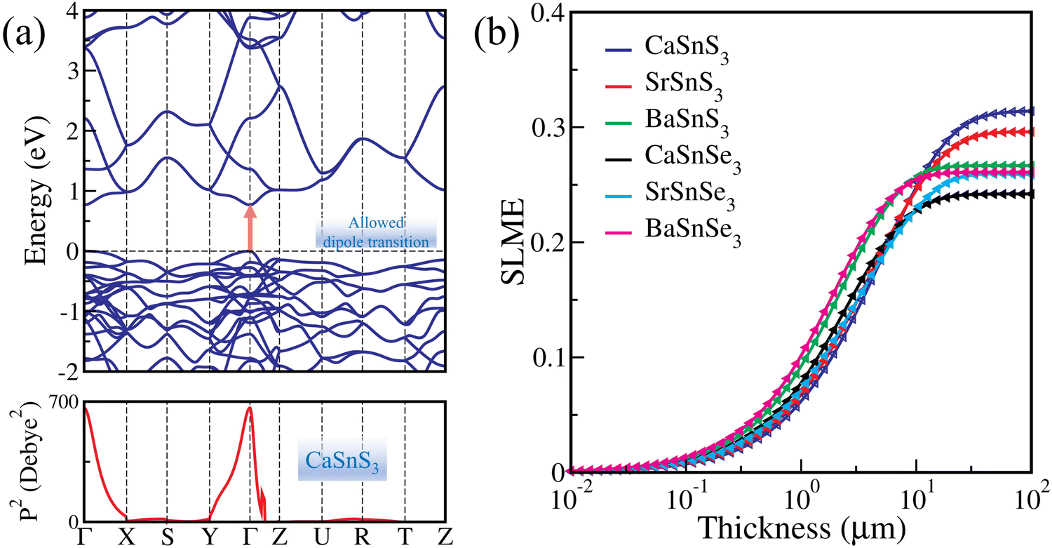 | ||
| Fig. 4 (a) Electronic band structure and transition probability (square of the transition dipole moment matrix elements) of CaSnS3 calculated using PBE, and (b) spectroscopic limited maximum efficiency (SLME) of ASnX3 (A = Ca, Sr, Ba; X = S, Se) chalcogenide perovskites calculated using the BSE@G0W0@PBE method. | ||
Next, the thickness dependence of SLME has been computed for all the ASnX3 (A = Ca, Sr, Ba; X = S, Se) compounds using the BSE@G0W0@PBE method and plotted in Fig. 4(b). It is clear that the SLME rises as the thickness increases and eventually saturates beyond a certain thickness. The maximum SLME is found to be 31.20% for CaSnS3, which is consistent with the previously documented theoretical efficiency of 32.45% at 10 μm thickness14 and is higher than CH3NH3PbI3 (28.97% at 2 μm).28 The highest SLME values for SrSnS3, BaSnS3, CaSnSe3, SrSnSe3, and BaSnSe3 compounds are calculated as 29.53%, 26.66%, 24.20%, 25.95%, and 26.09%, respectively. These values of SLME are favorable for the photovoltaic applications compared to transition metal-based traditional CPs and other halide perovskites14,15,22,78–80 (for details, see Table S14 of the ESI†).
3.7 Analysis of the SCAPS-1D results
To verify the photovoltaic potential of the investigated systems and our calculated SLME, we also conducted a detailed analysis using the solar cell capacitance simulator in 1 dimension (SCAPS-1D). This simulation allowed us to evaluate key performance metrics and gain deeper insights into the efficiency and operational behavior of the devices. Here, the performance of PSC is evaluated by varying the thickness of the absorber layer while keeping the ETL, HTL, and FTO thicknesses constant. The absorber layer thickness is varied from 0.01 μm to 1.2 μm, and it found that the thickness of the perovskite layer has a significant impact on the performance of the PSC [see Fig. 5(b)]. After reaching the optimum efficiency, the effect of the thickness of the perovskite layer seems to saturate, which agrees with our SLME calculations. The obtained results are summarized in Table 7. Our findings indicate that the device simulation results are consistent with the SLME work, specifically for ASnS3 (A = Ca, Sr, Ba). On the other hand, the minor discrepancies between the device simulation results for ASnSe3 (A = Ca, Sr, Ba) and the SLME findings may be attributed to the materials used in the ETL, HTL, and FTO layers. In our study, SLME provides an idealized efficiency limit based solely on the material's intrinsic optical properties, with its behavior improving for thicker films as absorption approaches a step function, aligning with the SQ limit. However, SCAPS-1D accounts for additional real-world effects, such as carrier transport, recombination losses, and device architecture, which can result in a performance decay for thicker films beyond 1 μm due to increased recombination or reduced carrier collection efficiency. This distinction highlights the necessity of combining both methods to achieve a comprehensive assessment of the material's optoelectronic potential, effectively bridging the gap between idealized theoretical predictions and practical device limitations. In general, SCAPS-1D proves to be a highly reliable software, as its simulation results confirm the high efficiency of the investigated materials, closely aligning with theoretical predictions. | ||
| Fig. 5 (a) Schematic of the simulated device structure and (b) power conversion efficiency (PCE) of the ASnX3 (A = Ca, Sr, Ba; X = S, Se) chalcogenide perovskite-based PSC using SCAPS-1D. | ||
| Optimized device | V oc (V) | J sc (mA cm−2) | FF (%) | PCE (%) |
|---|---|---|---|---|
| FTO/TiO2/CaSnS3/spiro-OMeTAD/Au | 1.2885 | 27.49796 | 89.63 | 31.76 |
| FTO/TiO2/SrSnS3/spiro-OMeTAD/Au | 1.3239 | 25.06713 | 90.15 | 29.92 |
| FTO/TiO2/BaSnS3/spiro-OMeTAD/Au | 0.9871 | 33.93041 | 86.49 | 28.97 |
| FTO/TiO2/CaSnSe3/spiro-OMeTAD/Au | 0.7255 | 55.85582 | 82.92 | 31.80 |
| FTO/TiO2/SrSnSe3/spiro-OMeTAD/Au | 0.7750 | 49.34989 | 83.80 | 32.05 |
| FTO/TiO2/BaSnSe3/spiro-OMeTAD/Au | 0.8050 | 43.53916 | 84.22 | 29.52 |
Overall, the study of all the above-discussed properties collectively shows that Se-based CaSnSe3 and SrSnSe3 demonstrate lower exciton binding energies and higher charge carrier mobilities than the rest of the investigated systems. However, their SLME is also relatively low. On the other hand, S-based CaSnS3 and SrSnS3 perovskites exhibit higher SLME despite having higher exciton binding energies and lower charge carrier mobilities compared to the other examined materials. This improved SLME is primarily attributed to the optimal bandgaps of CaSnS3 and SrSnS3 compared to their selenium (Se) counterparts, specifically from the perspective of solar cells. This reveals a trade-off between exciton binding energy, charge carrier mobility, and the bandgap of these materials. This suggests that integrating a combination of sulfur (S) and selenium (Se) atoms in these materials could be advantageous for potential application in solar cells, meriting further investigation.
4 Conclusions
In conclusion, we have carried out a comprehensive study to investigate the ground- and excited-state properties of post-transition metal Sn-based distorted chalcogenide perovskites (ASnX3; A = Ca, Sr, Ba, and X = S, Se) under the framework of state-of-the-art DFT combined with DFPT and MBPT (viz., GW and BSE). The mechanical properties confirm the stability, and Pugh's and Poisson's ratios reveal the ductile nature of these perovskites. The bandgaps calculated using the G0W0@PBE method are in the range of 0.79–1.50 eV, and the small effective masses of electrons suggest good charge carrier mobility, which is advantageous for energy-harvesting properties. Furthermore, they have a high optical absorption coefficient (>104 cm−1) and an optical bandgap extending from the near-infrared to the visible range, which is indicated by the BSE calculations. The exciton binding energies of these compounds, ranging from 0.04 to 0.23 eV, are similar to those of transition metal (Zr and Hf) based CPs. Also, these perovskites have smaller carrier-phonon coupling strengths than the conventional lead-based HPs as well as transition metal-based CPs, which leads to better polaron mobility for electrons (21.33–416.02 cm2 V−1 s−1) and holes (7.02–260.69 cm2 V−1 s−1). Additionally, the Fröhlich mesoscopic model implies that the charge-separated polaronic states have lower stability in comparison to bound excitons. Lastly, the SLME method forecasts that one could achieve the highest PCE of up to 31.20% by employing them, which is corroborated by conventional device (FTO/TiO2/ASnX3/spiro-OMeTAD/Au) simulations using SCAPS-1D software. The enhanced properties of Sn-based CPs can be attributed to the distinct valence state of Sn in comparison to transition metal-based CPs. Overall, these results are anticipated to expedite the research and use of chalcogenide perovskites in optoelectronic applications, in general, and solar cell technology, in particular.Data availability
The authors confirm that the data supporting the findings of this study are available within the article. Raw data were generated at Shiv Nadar Institution of Eminence. Derived data supporting the findings of this study are available from the corresponding author Priya Johari, on request.Conflicts of interest
There are no conflicts to declare.Acknowledgements
The authors would like to acknowledge the Council of Scientific and Industrial Research (CSIR), Government of India [Grant No. 3WS(007)/2023-24/EMR-II/ASPIRE] for financial support. S. A. would also like to acknowledge the CSIR, India [Grant No. 09/1128(11453)/2021-EMR-I] for the Senior Research Fellowship. S. D. thanks Prof. Marc Burgelman, Department of Electronics and Information Systems (ELIS), University of Gent, for providing the SCAPS-1D software. The authors acknowledge the High Performance Computing Cluster (HPCC) 'Magus' at Shiv Nadar Institution of Eminence for providing computational resources that have contributed to the research results reported within this paper.References
- D. Tiwari, O. S. Hutter and G. Longo, Chalcogenide perovskites for photovoltaics: current status and prospects, JPhys Energy, 2021, 3, 034010 CrossRef CAS.
- S. Niu, H. Huyan, Y. Liu, M. Yeung, K. Ye, L. Blankemeier, T. Orvis, D. Sarkar, D. J. Singh, R. Kapadia and J. Ravichandran, Bandgap Control via Structural and Chemical Tuning of Transition Metal Perovskite Chalcogenides, Adv. Mater., 2017, 29, 1604733 CrossRef PubMed.
- X. Wu, W. Gao, J. Chai, C. Ming, M. Chen, H. Zeng, P. Zhang, S. Zhang and Y.-Y. Sun, Defect tolerance in chalcogenide perovskite photovoltaic material BaZrS3, Sci. China: Mater., 2021, 64, 2976–2986 CAS.
- Y.-Y. Sun, M. L. Agiorgousis, P. Zhang and S. Zhang, Chalcogenide Perovskites for Photovoltaics, Nano Lett., 2015, 15, 581–585 CrossRef CAS PubMed.
- A. Kojima, K. Teshima, Y. Shirai and T. Miyasaka, Organometal Halide Perovskites as Visible-Light Sensitizers for Photovoltaic Cells, J. Am. Chem. Soc., 2009, 131, 6050–6051 CrossRef CAS PubMed.
- N.-G. Park, Organometal Perovskite Light Absorbers Toward a 20% Efficiency Low-Cost Solid-State Mesoscopic Solar Cell, J. Phys. Chem. Lett., 2013, 4, 2423–2429 CrossRef CAS.
- J. Berry, et al., Hybrid Organic-Inorganic Perovskites (HOIPs): Opportunities and Challenges, Adv. Mater., 2015, 27, 5102–5112 CrossRef CAS PubMed.
- D. A. Egger, A. M. Rappe and L. Kronik, Hybrid Organic-Inorganic Perovskites on the Move, Acc. Chem. Res., 2016, 49, 573–581 CrossRef CAS PubMed.
- D. B. Straus, S. Guo, A. M. Abeykoon and R. J. Cava, Understanding the Instability of the Halide Perovskite CsPbI3 through Temperature-Dependent Structural Analysis, Adv. Mater., 2020, 32, 2001069 CrossRef CAS PubMed.
- A. Babayigit, A. Ethirajan, M. Muller and B. Conings, Toxicity of organometal halide perovskite solar cells, Nat. Mater., 2016, 15, 247–251 CrossRef CAS PubMed.
- A. Swarnkar, W. J. Mir, R. Chakraborty, M. Jagadeeswararao, T. Sheikh and A. Nag, Are Chalcogenide Perovskites an Emerging Class of Semiconductors for Optoelectronic Properties and Solar Cell?, Chem. Mater., 2019, 31, 565–575 CrossRef CAS.
- K. V. Sopiha, C. Comparotto, J. A. Marquez and J. J. S. Scragg, Chalcogenide Perovskites: Tantalizing Prospects, Challenging Materials, Adv. Opt. Mater., 2022, 10, 2101704 CrossRef CAS.
- K. Kuhar, A. Crovetto, M. Pandey, K. S. Thygesen, B. Seger, P. C. K. Vesborg, O. Hansen, I. Chorkendorff and K. W. Jacobsen, Sulfide perovskites for solar energy conversion applications: computational screening and synthesis of the selected compound LaYS3, Energy Environ. Sci., 2017, 10, 2579–2593 RSC.
- P. Basera and S. Bhattacharya, Chalcogenide Perovskites (ABS3; A = Ba, Ca, Sr; B = Hf, Sn): An Emerging Class of Semiconductors for Optoelectronics, J. Phys. Chem. Lett., 2022, 13, 6439–6446 CrossRef CAS PubMed.
- S. Adhikari and P. Johari, Photovoltaic properties of ABSe3 chalcogenide perovskites (A = Ca, Sr, Ba; B = Zr, Hf), Phys. Rev. B, 2024, 109, 174114 CrossRef CAS.
- D. Liu, H. Zeng, H. Peng and R. Sa, Computational study of the fundamental properties of Zr-based chalcogenide perovskites for optoelectronics, Phys. Chem. Chem. Phys., 2023, 25, 13755–13765 RSC.
- R. Lelieveld and D. J. W. IJdo, Sulphides with the GdFeO3 structure, Acta Crystallogr., Sect. B, 1980, 36, 2223–2226 CrossRef.
- C.-S. Lee, K. Kleinke and H. Kleinke, Synthesis, structure, and electronic and physical properties of the two SrZrS3 modifications, Solid State Sci., 2005, 7, 1049–1054 CrossRef CAS.
- N. A. Moroz, C. Bauer, L. Williams, A. Olvera, J. Casamento, A. A. Page, T. P. Bailey, A. Weiland, S. S. Stoyko, E. Kioupakis, C. Uher, J. A. Aitken and P. F. P. Poudeu, Insights on the Synthesis, Crystal and Electronic Structures, and Optical and Thermoelectric Properties of Sr1−xSbxHfSe3 Orthorhombic Perovskite, Inorg. Chem., 2018, 57, 7402–7411 CrossRef CAS PubMed.
- L. J. Tranchitella, B.-H. Chen, J. C. Fettinger and B. W. Eichhorn, Structural Evolutions in the Sr1−xBaxZrSe3 Series, J. Solid State Chem., 1997, 130, 20–27 CrossRef CAS.
- S. Perera, H. Hui, C. Zhao, H. Xue, F. Sun, C. Deng, N. Gross, C. Milleville, X. Xu, D. F. Watson, B. Weinstein, Y.-Y. Sun, S. Zhang and H. Zeng, Chalcogenide perovskites-an emerging class of ionic semiconductors, Nano Energy, 2016, 22, 129–135 CrossRef CAS.
- M. Kumar, A. Singh, D. Gill and S. Bhattacharya, Optoelectronic Properties of Chalcogenide Perovskites by Many-Body Perturbation Theory, J. Phys. Chem. Lett., 2021, 12, 5301–5307 CrossRef CAS PubMed.
- H. M. Ghaithan, S. M. H. Qaid, Z. A. Alahmed, M. Hezam, A. Lyras, M. Amer and A. S. Aldwayyan, Anion Substitution Effects on the Structural, Electronic, and Optical Properties of Inorganic CsPb(I1−xBrx)3 and CsPb(Br1−xClx)3 Perovskites: Theoretical and Experimental Approaches, J. Phys. Chem. C, 2021, 125, 886–897 CrossRef CAS.
- R. Comin, G. Walters, E. S. Thibau, O. Voznyy, Z.-H. Lu and E. H. Sargent, Structural, optical, and electronic studies of wide-bandgap lead halide perovskites, J. Mater. Chem. C, 2015, 3, 8839–8843 RSC.
- X. Chen, H. Lu, Y. Yang and M. C. Beard, Excitonic Effects in Methylammonium Lead Halide Perovskites, J. Phys. Chem. Lett., 2018, 9, 2595–2603 CrossRef CAS PubMed PMID: 29714488.
- J. M. Frost, Calculating polaron mobility in halide perovskites, Phys. Rev. B, 2017, 96, 195202 CrossRef.
- Y. Kang and S. Han, Intrinsic Carrier Mobility of Cesium Lead Halide Perovskites, Phys. Rev. Appl., 2018, 10, 044013 CrossRef CAS.
- Q. Sun, H. Chen and W.-J. Yin, Do Chalcogenide Double Perovskites Work as Solar Cell Absorbers: A First-Principles Study, Chem. Mater., 2019, 31, 244–250 CrossRef CAS.
- H. Zou, Y. Duan, S. Yang, D. Xu, L. Yang, J. Cui, H. Zhou, M. Wu, J. Wang, X. Lei, N. Zhang and Z. Liu, 20.67%-Efficiency Inorganic CsPbI3 Solar Cells Enabled by Zwitterion Ion Interface Treatment, Small, 2023, 19, 2206205 CrossRef CAS PubMed.
- R. Guo and S. Wang, Anion-dependent Hot Carrier Dynamics in Chalcogenide Perovskites SrSnX3 (X = S, Se), J. Phys. Chem. C, 2019, 123, 29–35 CrossRef CAS.
- M.-G. Ju, J. Dai, L. Ma and X. C. Zeng, Perovskite Chalcogenides with Optimal Bandgap and Desired Optical Absorption for Photovoltaic Devices, Adv. Energy Mater., 2017, 7, 1700216 CrossRef.
- H. Shaili, M. Beraich, A. El hat, M. Ouafi, E. mehdi Salmani, R. Essajai, W. Battal, M. Rouchdi, M. Taibi, N. Hassanain and A. Mzerd, Synthesis of the Sn-based CaSnS3 chalcogenide perovskite thin film as a highly stable photoabsorber for optoelectronic applications, J. Alloys Compd., 2021, 851, 156790 CrossRef CAS.
- P. Hohenberg and W. Kohn, Inhomogeneous Electron Gas, Phys. Rev., 1964, 136, B864–B871 CrossRef.
- W. Kohn and L. J. Sham, Self-Consistent Equations Including Exchange and Correlation Effects, Phys. Rev., 1965, 140, A1133–A1138 CrossRef.
- M. Gajdoš, K. Hummer, G. Kresse, J. Furthmüller and F. Bechstedt, Linear optical properties in the projector-augmented wave methodology, Phys. Rev. B: Condens. Matter Mater. Phys., 2006, 73, 045112 CrossRef.
- H. Jiang, P. Rinke and M. Scheffler, Electronic properties of lanthanide oxides from the GW perspective, Phys. Rev. B: Condens. Matter Mater. Phys., 2012, 86, 125115 CrossRef.
- F. Fuchs, C. Rödl, A. Schleife and F. Bechstedt, Efficient O(N2) approach to solve the Bethe–Salpeter equation for excitonic bound states, Phys. Rev. B: Condens. Matter Mater. Phys., 2008, 78, 085103 CrossRef.
- J. P. Perdew, K. Burke and M. Ernzerhof, Generalized Gradient Approximation Made Simple, Phys. Rev. Lett., 1996, 77, 3865–3868 CrossRef CAS PubMed.
- J. Heyd, G. E. Scuseria and M. Ernzerhof, Hybrid functionals based on a screened Coulomb potential, J. Chem. Phys., 2003, 118, 8207–8215 CrossRef CAS.
- L. Hedin, New Method for Calculating the One-Particle Green's Function with Application to the Electron-Gas Problem, Phys. Rev., 1965, 139, A796–A823 CrossRef.
- M. S. Hybertsen and S. G. Louie, First-Principles Theory of Quasiparticles: Calculation of Band Gaps in Semiconductors and Insulators, Phys. Rev. Lett., 1985, 55, 1418–1421 CrossRef CAS PubMed.
- S. Albrecht, L. Reining, R. Del Sole and G. Onida, Ab Initio Calculation of Excitonic Effects in the Optical Spectra of Semiconductors, Phys. Rev. Lett., 1998, 80, 4510–4513 CrossRef CAS.
- M. Rohlfing and S. G. Louie, Electron-Hole Excitations in Semiconductors and Insulators, Phys. Rev. Lett., 1998, 81, 2312–2315 CrossRef CAS.
- L. Yu and A. Zunger, Identification of Potential Photovoltaic Absorbers Based on First-Principles Spectroscopic Screening of Materials, Phys. Rev. Lett., 2012, 108, 068701 CrossRef PubMed.
- A. Husainat, W. Ali, P. Cofie, J. Attia and J. Fuller, Simulation and Analysis of Methylammonium Lead Iodide (CH3NH3PbI3) Perovskite Solar Cell with Au Contact Using SCAPS 1D Simulator, Am. J. Opt. Photonics, 2019, 7, 33–40 CrossRef.
- M. K. Hossain, A. A. Arnab, D. P. Samajdar, M. H. K. Rubel, M. M. Hossain, M. R. Islam, R. C. Das, H. Bencherif, M. F. Rahman, J. Madan, R. Pandey, S. Bhattarai, M. Amami and D. K. Dwivedi, Design Insights into La2NiMnO6-Based Perovskite Solar Cells Employing Different Charge Transport Layers: DFT and SCAPS-1D Frameworks, Energy Fuels, 2023, 37, 13377–13396 CrossRef CAS.
- S. S. Nishat, M. J. Hossain, F. E. Mullick, A. Kabir, S. Chowdhury, S. Islam and M. Hossain, Performance Analysis of Perovskite Solar Cells Using DFT-Extracted Parameters of Metal-Doped TiO2 Electron Transport Layer, J. Phys. Chem. C, 2021, 125, 13158–13166 CrossRef CAS.
- S. Ramawat, S. Kukreti, D. J. Sapkota and A. Dixit, Insight into the Microband Offset and Charge Transport Layer's Suitability for an Efficient Inverted Perovskite Solar Cell: A Case Study for Tin-Based B-CsSnI3, Energy Fuels, 2024, 38, 9011–9026 CrossRef CAS.
- G. Kresse and J. Furthmüller, Efficient iterative schemes for ab initio total-energy calculations using a plane-wave basis set, Phys. Rev. B: Condens. Matter Mater. Phys., 1996, 54, 11169–11186 CrossRef CAS PubMed.
- G. Kresse and J. Furthmüller, Efficiency of Ab-initio Total Energy Calculations for Metals and Semiconductors Using a Plane-wave Basis Set, Comput. Mater. Sci., 1996, 6, 15–50 CrossRef CAS.
- P. E. Blöchl, Projector augmented-wave method, Phys. Rev. B: Condens. Matter Mater. Phys., 1994, 50, 17953–17979 CrossRef PubMed.
- K. Momma and F. Izumi, VESTA3 for three-dimensional visualization of crystal, volumetric and morphology data, J. Appl. Crystallogr., 2011, 44, 1272–1276 CrossRef CAS.
- A. Togo, L. Chaput, T. Tadano and I. Tanaka, Implementation strategies in phonopy and phono3py, J. Phys.: Condens. Matter, 2023, 35, 353001 CrossRef CAS PubMed.
- A. M. Ganose, A. J. Jackson and D. Scanlon, O. sumo: command-line tools for plotting and analysis of periodic ab initio calculations, J. Open Source Software, 2018, 3, 717 CrossRef.
- V. Wang, N. Xu, J.-C. Liu, G. Tang and W.-T. Geng, VASPKIT: a user-friendly interface facilitating high-throughput computing and analysis using VASP code, Comput. Phys. Commun., 2021, 267, 108033 CrossRef CAS.
- S. Adhikari and P. Johari, Theoretical insights into monovalent–metal–cation transmutation effects on lead-free halide double perovskites for optoelectronic applications, Phys. Rev. Mater., 2023, 7, 075401 CrossRef CAS.
- M. R. Filip, J. B. Haber and J. B. Neaton, Phonon Screening of Excitons in Semiconductors: halide Perovskites and Beyond, Phys. Rev. Lett., 2021, 127, 067401 CrossRef CAS PubMed.
- R. W. Hellwarth and I. Biaggio, Mobility of an electron in a multimode polar lattice, Phys. Rev. B: Condens. Matter Mater. Phys., 1999, 60, 299–307 CrossRef CAS.
- M. Jain, P. Bhumla, M. Kumar and S. Bhattacharya, Lead-Free Alloyed Double Perovskites: An Emerging Class of Materials for Optoelectronic Applications, J. Phys. Chem. C, 2022, 126, 6753–6760 CrossRef CAS.
- R. P. Feynman, Slow Electrons in a Polar Crystal, Phys. Rev., 1955, 97, 660–665 CrossRef CAS.
- M. Burgelman, P. Nollet and S. Degrave, Modelling polycrystalline semiconductor solar cells, Thin Solid Films, 2000, 361–362, 527–532 CrossRef CAS.
- M. Burgelman, K. Decock, S. Khelifi and A. Abass, Advanced electrical simulation of thin film solar cells, Thin Solid Films, 2013, 535, 296–301 CrossRef CAS.
- C. Li, X. Lu, W. Ding, L. Feng, Y. Gao and Z. Guo, Formability of ABX3 (X = F, Cl, Br, I) halide perovskites, Acta Crystallogr., 2008, 64, 702–707 CAS.
- C. J. Bartel, C. Sutton, B. R. Goldsmith, R. Ouyang, C. B. Musgrave, L. M. Ghiringhelli and M. Scheffler, New tolerance factor to predict the stability of perovskite oxides and halides, Sci. Adv., 2019, 5, eaav0693 CrossRef CAS PubMed.
- F. Mouhat and F.-X. Coudert, Necessary and sufficient elastic stability conditions in various crystal systems, Phys. Rev. B: Condens. Matter Mater. Phys., 2014, 90, 224104 CrossRef.
- Z.-J. Wu, E.-J. Zhao, H.-P. Xiang, X.-F. Hao, X.-J. Liu and J. Meng, Crystal structures and elastic properties of superhard IrN2 and IrN3 from first principles, Phys. Rev. B: Condens. Matter Mater. Phys., 2007, 76, 054115 CrossRef.
- R. Hill, The Elastic Behaviour of a Crystalline Aggregate, Proc. Phys. Soc., London, Sect. A, 1952, 65, 349–354 CrossRef.
- S. X. C. I. I. Pugh, Relations between the elastic moduli and the plastic properties of polycrystalline pure metals, London, Edinburgh Dublin Philos. Mag. J. Sci., 1954, 45, 823–843 CrossRef CAS.
- M. Mattesini, M. Magnuson, F. Tasnádi, C. Höglund, I. A. Abrikosov and L. Hultman, Elastic properties and electrostructural correlations in ternary scandium-based cubic inverse perovskites: a first-principles study, Phys. Rev. B: Condens. Matter Mater. Phys., 2009, 79, 125122 CrossRef.
- X. Liu, B. Xie, C. Duan, Z. Wang, B. Fan, K. Zhang, B. Lin, F. J. M. Colberts, W. Ma, R. A. J. Janssen, F. Huang and Y. Cao, A high dielectric constant non-fullerene acceptor for efficient bulk-heterojunction organic solar cells, J. Mater. Chem. A, 2018, 6, 395–403 RSC.
- X. Wang, W. Meng and Y. Yan, Electronic band structures and excitonic properties of delafossites: a GW–BSE study, J. Appl. Phys., 2017, 122, 085104 CrossRef.
- F. Ferreira, A. J. Chaves, N. M. R. Peres and R. M. Ribeiro, Excitons in hexagonal boron nitride single-layer: a new platform for polaritonics in the ultraviolet, J. Opt. Soc. Am. B, 2019, 36, 674–683 CrossRef CAS.
- S. Adhikari and P. Johari, Capturing optoelectronic properties of Cs2AgSbBr6−xClx (x = 0–6) double perovskites using many-body perturbation theory, Phys. Rev. B, 2024, 110, 014101 CrossRef CAS.
- M. Bokdam, T. Sander, A. Stroppa, S. Picozzi, D. D. Sarma, C. Franchini and G. Kresse, Role of Polar Phonons in the Photo Excited State of Metal Halide Perovskites, Sci. Rep., 2016, 6, 28618 CrossRef CAS PubMed.
- C. D. Spataru and F. Leonard, Quasiparticle and exciton renormalization effects in electrostatically doped semiconducting carbon nanotubes, Chem. Phys., 2013, 413, 81–88 CrossRef CAS.
- H. Fröhlich, Electrons in lattice fields, Adv. Phys., 1954, 3, 325–361 CrossRef.
- W. Shockley and H. J. Queisser, Detailed Balance Limit of Efficiency of p–n Junction Solar Cells, J. Appl. Phys., 2004, 32, 510–519 CrossRef.
- A. C. Dias, M. P. Lima and J. L. F. Da Silva, Role of Structural Phases and Octahedra Distortions in the Optoelectronic and Excitonic Properties of CsGeX3 (X = Cl, Br, I) Perovskites, J. Phys. Chem. C, 2021, 125, 19142–19155 CrossRef CAS.
- J. Qian, B. Xu and W. Tian, A comprehensive theoretical study of halide perovskites ABX3, Org. Electron., 2016, 37, 61–73 CrossRef CAS.
- J. Kangsabanik, V. Sugathan, A. Yadav, A. Yella and A. Alam, Double perovskites overtaking the single perovskites: a set of new solar harvesting materials with much higher stability and efficiency, Phys. Rev. Mater., 2018, 2, 055401 CrossRef CAS.
Footnote |
| † Electronic supplementary information (ESI) available. See DOI: https://doi.org/10.1039/d4tc04701j |
| This journal is © The Royal Society of Chemistry 2025 |