
 Open Access Article
 This Open Access Article is licensed under a Creative Commons Attribution-Non Commercial 3.0 Unported Licence
Doubling the efficiency of solution-processed blue phosphorescent organic light-emitting diodes via modified PEDOT![[thin space (1/6-em)]](https://www.rsc.org/images/entities/h2_char_2009.gif) :PSS hole-injection layers†
:PSS hole-injection layers†
Jingyu
Wang
ab,
Tingyu
Pan
a,
Tongtong
Zhang
ab,
Danyang
Zhang
ab,
Guibin
Wang
 *c and
Liang
Zhou
*ab
*c and
Liang
Zhou
*ab
aState Key Laboratory of Rare Earth Resource Utilization, Changchun Institute of Applied Chemistry, Chinese Academy of Sciences, Changchun 130022, People's Republic of China. E-mail: zhoul@ciac.ac.cn
bUniversity of Science and Technology of China, Hefei 230027, People's Republic of China
cCollege of Chemistry, Key Laboratory of High Performance Plastics, Ministry of Education, Jilin University, Changchun, 130022, People's Republic of China. E-mail: wgb@jlu.edu.cn
First published on 29th January 2025
Abstract
For solution-processed organic light-emitting diodes (OLEDs), poly(3,4-ethylenedioxythiophene):poly(styrenesulfonate) (PEDOT![[thin space (1/6-em)]](https://www.rsc.org/images/entities/char_2009.gif) :PSS) is commonly utilized as the hole injection layer due to its superior conductivity, transparency, and excellent film-forming properties. Compared to the excellent performance of red and green OLEDs, low efficiency in blue OLEDs is the bottleneck because of the large hole injection barrier caused by the wide bandgap of blue phosphorescent materials and their mismatched energy levels with PEDOT:PSS. To optimize device performance, a simple and cost-effective strategy was devised by incorporating various dopants such as PSSA, PSSNa, and PSSNH4 into PEDOT:PSS films. Due to the formation of the PSS layer and the promotion of conduction via cationic carriers, coupled with the utilization of the exciplex as the host, the optimal device exhibited the maximum external quantum efficiency (EQE) of 21.33%, nearly doubling the efficiency of the original device (11.88%). The turn-on voltage was reduced from approximately 3.9 V to about 3.5 V. Additionally, the FIrpic-based blue phosphorescent device achieved the maximum EQE of up to 24.18%, which, to the best of our knowledge, represents the highest value recorded for solution-processed OLEDs based on FIrpic.
:PSS) is commonly utilized as the hole injection layer due to its superior conductivity, transparency, and excellent film-forming properties. Compared to the excellent performance of red and green OLEDs, low efficiency in blue OLEDs is the bottleneck because of the large hole injection barrier caused by the wide bandgap of blue phosphorescent materials and their mismatched energy levels with PEDOT:PSS. To optimize device performance, a simple and cost-effective strategy was devised by incorporating various dopants such as PSSA, PSSNa, and PSSNH4 into PEDOT:PSS films. Due to the formation of the PSS layer and the promotion of conduction via cationic carriers, coupled with the utilization of the exciplex as the host, the optimal device exhibited the maximum external quantum efficiency (EQE) of 21.33%, nearly doubling the efficiency of the original device (11.88%). The turn-on voltage was reduced from approximately 3.9 V to about 3.5 V. Additionally, the FIrpic-based blue phosphorescent device achieved the maximum EQE of up to 24.18%, which, to the best of our knowledge, represents the highest value recorded for solution-processed OLEDs based on FIrpic.
1. Introduction
In the past decade, organic light-emitting diodes (OLEDs) have emerged as the most gorgeous display technology with applications in smartphones, televisions, and lighting devices.1,2 The advancement of OLED technology is intricately linked to innovations in luminescent materials and device structures. Compared to traditional fluorescent materials, phosphorescent materials can utilize the energy of both singlet and triplet excitons, thereby significantly improving the device performance.3–5 Furthermore, solution-processed OLEDs present several compelling advantages, including cost-effectiveness, suitability for large-area fabrication, and simplicity in production processes.6,7 It is anticipated that this method will play an increasingly pivotal role in industrial production. At present, while green and red OLEDs have demonstrated excellent performance, blue OLEDs, especially the solution-processed blue OLEDs, remain a critical bottleneck in OLED technology development due to their relatively low efficiency, shorter operation lifetime, and inferior stability.8–10 The blue phosphorescent materials with a wide bandgap necessitate higher driving voltages for charge injection into the emissive layer, which not only increases energy consumption but also potentially induces device heating, thereby accelerating material degradation.11,12 These problems limit the practical applications of solution-processed blue phosphorescent OLEDs (PhOLEDs) due to unsatisfactory performance and reliability. Consequently, addressing these problems necessitates further optimization of device structures to achieve wider applications.Generally, for solution-processed devices, poly(3,4-ethylenedioxythiophene):poly(styrenesulfonate) (PEDOT:PSS) is the most utilized hole injection layer owing to its high conductivity, transparency, and excellent film-forming properties.13 Nonetheless, the mismatch between the highest occupied molecular orbital (HOMO) level of blue phosphorescent emitters (∼−6.1 eV) and that of PEDOT:PSS results in a formidable hole injection barrier, reducing the efficiency of hole injection into a light-emitting layer (EML). Furthermore, the strongly acidic nature of PEDOT:PSS films can corrode the indium tin oxide (ITO) anode as well as the EML, which further deteriorates device performance.14 To improve the hole injection/transport capabilities, various effective strategies have been explored, such as the utilization of cross-linked hole transport layers (HTL) and a modified PEDOT:PSS (m-PEDOT:PSS) hole injection layer (HIL). The cross-linked HTL formed through curing reactions exhibits excellent solvent resistance. However, this typically requires additional processes such as thermal annealing or photo-crosslinking, thereby increasing complexity and cost of fabrication.15,16 By contrast, blending additives into a PEDOT:PSS layer to adjust its properties is comparatively simpler and more cost-effective. Lee and colleagues have demonstrated that the incorporation of tetrafluoroethyleneperfluoro-3,6-dioxa-4-methyl-7-octene-sulfonic acid copolymer (PFI) into the PEDOT:PSS layer results in the formation of a self-organized buffering HIL, which reduces the hole injection barrier.17,18 This modification significantly increases hole injection capability and improves device performance. Furthermore, the HIL can be further optimized by controlling the PSS to PEDOT surface ratio to achieve high-performance devices. Greczynski et al. found the formation of a PSS-rich surface layer in PEDOT:PSS with a molar ratio of PEDOT to PSS of 0.8.19 Several hypotheses have been proposed to elucidate the mechanistic role of PSS in HIL improvement. Primarily, the surface concentration of the PSS dopant can tune the work function.20 Yang and associates reduced the hole injection barrier by doping poly(4-styrenesulfonic acid) (PSSA) into PEDOT:PSS, thus realizing a record-breaking EQE in solution-processed OLEDs based on 4CzIPN and FIrpic.21 Furthermore, the PSS-rich insulating layer effectively prevents electron injection into the PEDOT:PSS layer, significantly suppressing electron leakage current. The insulating layer provides a barrier for electron extraction, and the accumulation of electron density enhances the electric field, thus effectively facilitating hole injection.22–26 For instance, Wang et al. used low-conductivity Baytron P CH 8000 (PEDOT:PSS ratio of 1:20) instead of Baytron P Al 4083 (PEDOT:PSS ratio of 1:6) as the HIL, achieving a world-record EQE of 26.0% at a luminance of 100 cd m−2 for solution-processed WOLEDs.27 Cao et al. also used this material to reduce the turn-on voltage from 3.4 to 2.8 V.28 However, increasing the PSS content also resulted in the decreased conductivity of the HIL, which restricted further device performance improvements.29 Crispin et al. first investigated the effects of doping poly(sodium styrenesulfonate) (PSSNa) into PEDOT:PSS on its electrical and ionic conductivity, and demonstrated that Na ions could modulate the conductivity of PEDOT:PSS-PSSNa through ionic conduction mechanisms.30,31 Mathews et al. demonstrated that auxiliary ionic conductivity imparted by Na ions.32 Moreover, Huang et al. significantly improved the device performance by constructing PSS aggregates and increasing the interfacial contact area through NH3 vapour annealing to convert a portion of PSS into ammonium salt and thermal imprinting treatment to form sub-micron sized stripes in the PEDOT:PSS HIL.33
To achieve high efficiency blue phosphorescent devices, the selected host materials should have not only high enough triplet energies (T1) (to ensure efficient energy transfer) but also appropriate energy levels and bipolar transport properties (to improve carrier injection and balance).34,35 In this study, tunable bipolar interfacial exciplexes were designed as hosts capable of adjusting the behavior of donor and acceptor molecules. As a result, decreased turn-on voltage and improved device efficiency were realized. Furthermore, the effect of incorporating various poly(styrene sulfonate) (PSS-S; PSSA, PSSNa, and PSSNH4) into PEDOT:PSS on the performance of blue phosphorescent OLEDs was also studied. The presence of a PSS-rich insulating layer was demonstrated by X-ray photoelectron spectroscopy (XPS) analysis. To elucidate the hole injection and transport mechanisms in m-PEDOT:PSS, we employed various characterization methods such as ultraviolet photoelectron spectroscopy (UPS), hole-only devices testing, and transient electroluminescence (EL) decay curves. Furthermore, we systematically investigated the surface morphology of m-PEDOT:PSS films and the effect on the EML using atomic force microscopy (AFM) and transient photoluminescence (PL) decay curves. Comparatively, lower efficiencies of the device based on cross-linkable hole transport materials (HTMs) underscore that the use of m-PEDOT:PSS films is a simple and cost-effective strategy. Our experimental results demonstrated that the PSS-rich surface layer acts to suppress leakage current and increase hole injection, and the cation acts as an auxiliary ionic conductor, which synergistically enhance the performance of blue PhOLEDs. As a result, the bis(2,4-difluorophenylpyridinato)tetrakis(1-pyrazolyl)borate iridium(III) (FIr6)-based blue phosphorescent device achieved decreased turn-on voltage from 3.9 to 3.5 V and the maximum external quantum efficiency (EQE) of 21.33%, which is about twice that of original device (11.88%). The FIrpic-based blue phosphorescent device attained a remarkably high maximum EQE of 24.18%, which is the highest value reported so far for solution-processed OLEDs based on corresponding emitters.
2. Results and discussion
Devices with the structures of ITO/PEDOT:PSS (30 nm)/TCTA:FIr6 (20 nm)/TmPyPB or POPH (20 nm)/1,3,5-tri[(3-pyridyl)-phen-3-yl]benzene (TmPyPB) (40 nm)/LiF (1 nm)/Al (100 nm) (devices B0 and B1) were fabricated by utilizing 20 wt% FIr6 as the blue emitter. The high triplet energies of 4,4′′,4′′-tris(carbazol-9-yl)triphenylamine (TCTA) and (5-terphenyl-1,3-phenylene)bis(diphenylphosphine oxide) (POPH) (2.80 and 2.78 eV, respectively) were selected as the donor and acceptor (D and A), respectively. The energy levels diagram of the devices, along with its corresponding molecular and devices structures, are shown in Fig. 1a and Fig. S1 and S2 (ESI†), respectively. In Fig. 1b, the PL spectrum of TCTA:POPH film (1:1 molar ratio) reveals a significantly red-shifted emission peak at 432 nm compared to the spectra of pure TCTA and POPH films. Additionally, a bi-exponential decay with prompt and delayed lifetimes of approximately 15.90 and 54.37 ns, respectively, was observed, indicating the presence of intermolecular interactions within the excited states of the exciplex (Fig. 1c). The PL spectrum of TCTA:TmPyPB films did not exhibit a redshift relative to that of TCTA, and their lifetimes were only a few nanoseconds, demonstrating the absence of exciplex formation between TCTA and TmPyPB (Fig. S3, ESI†). Furthermore, no new bands were observed in the absorption spectra of the TCTA:POPH film, implying that there are no ground state interactions between these molecules (Fig. S4, ESI†). The lowest singlet energy (S1) and T1 of the TCTA:POPH exciplex were estimated to be 2.87 and 2.68 eV, respectively, based on the fluorescence spectrum measured at 300 K and the phosphorescence spectrum measured at 77 K. To further corroborate the formation of an exciplex near TCTA/POPH interface under electrical excitation, an undoped device was fabricated for comparison. This device exhibited EL spectrum featuring a new emission at 433 nm, which corresponds to the PL spectrum of exciplex, indicating that TCTA and POPH can directly form an interfacial exciplex (Fig. 1d). To ascertain the suitability of designing an exciplex as a host for blue phosphorescent emitters, energy transfer processes between the exciplex TCTA:POPH and FIr6 as well as FIrpic were investigated. As shown in Fig. S5 (ESI†), the emission spectrum of the exciplex strongly overlaps with the absorption spectra of both FIr6 and FIrpic, suggesting that efficient Förster resonance energy transfer (FRET) between them is possible.
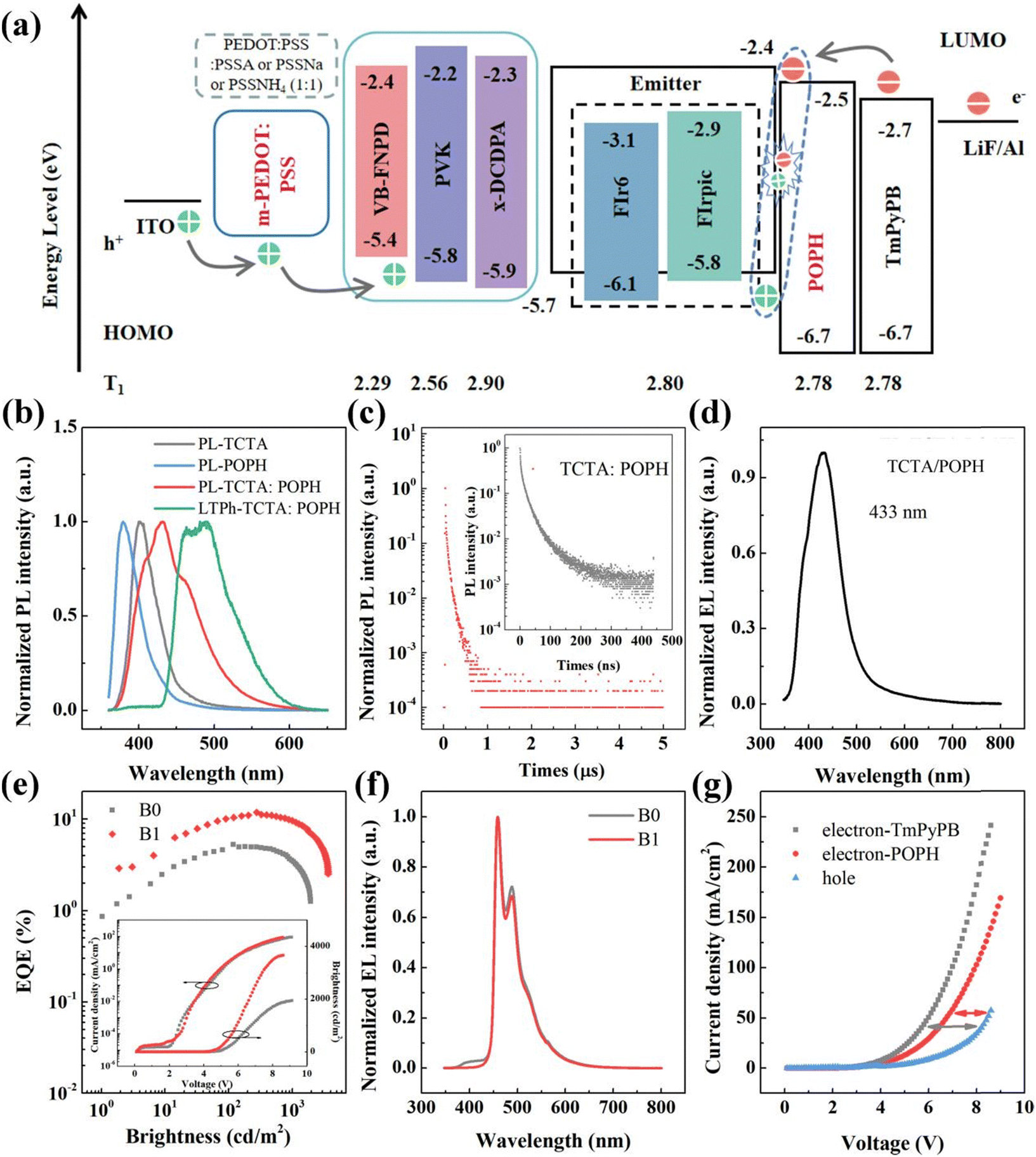 | ||
| Fig. 1 (a) The energy levels diagram of all blue devices. (b) PL and low-temperature phosphorescence spectra of TCTA, POPH, and TCTA:POPH films. (c) Transient PL decay curve of the TCTA:POPH film under 300 nm excitation. Inset: Transient PL decay curve with prompt lifetime. (d) EL spectra of TCTA/POPH exciplex devices. (e) EQE-brightness characteristics of B0 and B1. Inset: Current density–voltage–brightness characteristics of B0 and B1. (f) EL spectra of B0 and B1 operating at 10 mA cm−2. (g) Current density–voltage characteristics of hole-only and electron-only devices. | ||
The device based on the interfacial exciplex demonstrated superior performance with the maximum current efficiency (CE) of 19.94 cd A−1, maximum power efficiency (PE) of 12.28 lm W−1, maximum EQE of 11.88%, and maximum brightness of 3670 cd m−2 (Fig. 1e and Table 1). Compared with the reference device (B0), the interfacial exciplex-host-based device (B1) exhibited emission peaks exclusively from FIr6 without exciplex emission, which was attributed to the efficient energy transfer from the interfacial exciplex to FIr6 (Fig. 1f). In addition, to further elucidate the underlying factors influencing device performance, both the triplet energies of the interfacial exciplex and the carrier transport properties of POPH were investigated in detail. It was found that TCTA and TmPyPB cannot form an exciplex and that TCTA exhibits higher triplet energy, thus preventing the reverse energy transfer from emitters to host. However, the maximum EQE of device B0 is merely 5.28%, indicating that triplet energy of the TCTA:POPH exciplex host material (comparable to that of FIr6) is not the only factor influencing device performance. Subsequently, electron-only devices (EODs) and hole-only devices (HODs) were prepared and compared. The decreased current density of POPH-based EOD exhibits small difference with that of HOD, which is attributed to the fact that the presence of POPH as the partial electron transport layer (ETL) retards electron transport and thus facilitates carrier balance (Fig. 1g). Therefore, the superior performance of the device based on the TCTA/POPH interfacial exciplex can be elucidated by two primary factors: its elevated triplet energy and improved carrier balance.
| Device | V on (V) | CEmax/1000a (cd A−1) | PEmax/1000b (lm W−1) | EQEmax/1000c (%) | B max (cd m−2) | EQE roll-offe | CIE |
|---|---|---|---|---|---|---|---|
| a The data for maximum current efficiency and values taken at 1000 cd m−2 (CE). b Maximum power efficiency and values taken at 1000 cd m−2 (PE). c Maximum external quantum efficiency and values taken at 1000 cd m−2 (EQE). d Maximum brightness (B). e EQE roll-off = (EQEmax − EQE1000)/EQEmax × 100%. | |||||||
| B0 | 4.1 | 8.92 (5.99) | 5.39 (2.81) | 5.28 (3.56) | 1950 | 32.45 | (0.159, 0.243) |
| B1 | 3.9 | 19.94 (16.05) | 12.28 (8.55) | 11.88 (9.59) | 3670 | 19.28 | (0.155, 0.237) |
| B1-H | 3.5 | 30.04 (16.59) | 26.96 (11.84) | 17.29 (10.44) | 3038 | 39.62 | (0.148, 0.226) |
| B1-Na | 3.5 | 36.48 (26.19) | 29.38 (16.79) | 21.33 (15.15) | 5020 | 28.97 | (0.145, 0.263) |
| B1-NH4 | 3.5 | 31.58 (19.61) | 27.56 (14.67) | 18.12 (12.13) | 4378 | 33.06 | (0.148, 0.231) |
| B1-V | 2.9 | 27.56 (22.18) | 27.05 (13.15) | 16.30 (12.96) | 5960 | 20.49 | (0.148, 0.257) |
| B1-P | 3.9 | 21.32 (18.30) | 13.13 (10.08) | 12.56 (10.82) | 4223 | 13.85 | (0.158, 0.237) |
| B1-X | 4.1 | 20.49 (17.08) | 12.14 (8.80) | 12.38 (10.38) | 4017 | 16.16 | (0.154, 0.233) |
| B2 | 3.5 | 23.43 (15.19) | 20.40 (10.85) | 14.02 (8.85) | 3356 | 36.88 | (0.160, 0.242) |
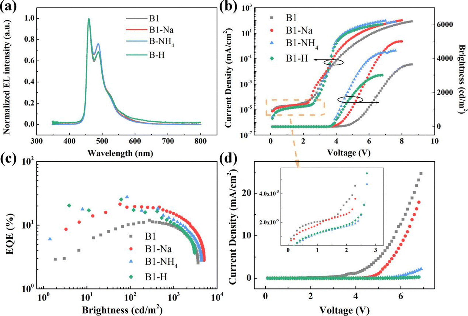
Generally, PEDOT:PSS is the most widely adopted hole-injection material in solution-processed OLEDs. However, the energy level mismatch with blue phosphorescent materials results in a large hole injection barrier, which inhibits hole injection efficiency. For example, a solution-processed blue phosphorescent device based on FIrpic (with a higher HOMO level of −5.7 eV; device B3 in Fig. S2, ESI†) with the same structure as the FIr6-based device exhibits the maximum EQE of 14.89%, which markedly surpassed that (11.88%) of the device based on FIr6 (with lower HOMO level of −6.1 eV; device B1 in Fig. S2, ESI†). To achieve superior device performance, an m-PEDOT:PSS strategy was proposed by mixing PEDOT:PSS with PSSNa, PSSNH4, and PSSA (v/v = 1:1), respectively to optimize HIL and consequently enhance hole injection. Herein, different concentrations of PSSA (from 20 to 100 mg mL−1 with step of 20 mg mL−1; v/v = 1:1) were added into PEDOT:PSS to identify the optimal formulation. The device doped with 80 mg mL−1 PSSA (device B1-H in Fig. S2, ESI†) exhibited the highest performance with a maximum EQE of 17.29% (30.04 cd A−1, 26.96 lm W−1, 3038 cd m−2). Furthermore, this device showed lower turn-on voltage (defined as the needed drive voltage at the brightness of 1 cd m−2) of 3.5 V. Then, PSSNa and poly(ammonium styrenesulfonate) (PSSNH4) were also utilized to modify PEDOT:PSS. Several devices were prepared by mixing PEDOT:PSS with PSSNa (from 20 to 100 mg mL−1 with step of 20 mg mL−1; v/v = 1:1) or PSSNH4 (from 20 to 60 mg mL−1 with step of 10 mg mL−1; v/v = 1:1). The devices based on m-PEDOT:PSS with PSSNa (60 mg mL−1, device B1-Na in Fig. S2, ESI†) and PSSNH4 (40 mg mL−1, device B1-NH4 in Fig. S2, ESI†) achieved the maximum EQEs of 21.33% (36.48 cd A−1, 29.38 lm W−1 and 5020 cd m−2) and 18.12% (31.58 cd A−1, 27.56 lm W−1 and 4378 cd m−2), respectively, with turn-on voltages around 3.5 V. The decrease in turn-on voltage suggests that the m-PEDOT:PSS facilitates more efficient hole injection. We speculate that the incorporation of PSS-S forms a PSS surface layer, which may reduce the hole injection barrier between the HIL and the EML by tuning the work function, or enhance the electric field by providing a barrier to accumulate electrons, thus facilitating hole injection. However, as shown in Fig. 2c and Table 1, the devices based on m-PEDOT:PSS displayed more severe efficiency roll-off compared to the device with a pristine PEDOT:PSS. This indicates that charge balance is only achievable under low current density conditions. Additionally, this phenomenon may be attributed to the narrow exciton recombination zone, which enhanced exciton density thus causing increased exciton quenching.36
 | ||
| Fig. 2 Performances of FIr6-based blue phosphorescent devices with various PSS-S incorporated in PEDOT:PSS. (a) EL spectra of these devices operating at 10 mA cm−2. (b) Current density–voltage–brightness characteristics of these devices. (c) EQE-brightness characteristics of these devices. (d) Current density–voltage characteristics of hole-only devices. Inset: Enlarged view of current density–voltage characteristics between 0 V and 3 V of Fig. 2b. | ||
To substantiate the modification effects of PSS-S on PEDOT:PSS, we performed UPS measurement on both the pristine and modified PEDOT:PSS films. The ionization potential (IP) changes of the different modified PEDOT:PSS films were further elucidated by measuring the work function (WF) and valence band maximum (VBM).32,37,38 As shown in Fig. 3a, b and Table 2, the incorporation of PSSNa, PSSNH4, and PSSA results in a reduction of the WF from 4.48 to 4.30, 4.19 and 3.67 eV, respectively, while the VBM shifts from 0.74 to 1.16, 1.16 and 1.60 eV, correspondingly. Consequently, the IP increases from 5.22 to 5.46, 5.35 and 5.27 eV. This change decreases the hole injection barrier with FIr6 (−6.1 eV) from 0.88 to 0.64, 0.75 and 0.83 eV, respectively. The experimental results obtained through UPS measurements indicate that the reduced hole injection barrier facilitates hole injection. Interestingly, as shown in Fig. 2d, the hole-only devices incorporating various PSS-S demonstrate a decrease in hole current density. This phenomenon can be attributed to the PSS-rich layer on the surface of m-PEDOT:PSS, which leads to ineffective hole injection and reduces the conductivity due to the insulating nature of PSS.20 However, the m-PEDOT:PSS-based devices did exhibit lower turn-on voltages compared to the pristine PEDOT:PSS devices, suggesting that hole injection remains efficacious in m-PEDOT:PSS-based devices. We speculate that another mechanism may effectively enhance hole injection. Specifically, the PSS insulating layer provides barrier to electron extraction at the anode, and the accumulation of electron density increases the electric field, thus facilitating hole injection. It is important to note that this enhancement in hole injection is contingent upon the presence of injected electrons.22,24,26,28
 | ||
| Fig. 3 The photoelectron spectra of pristine and modified PEDOT:PSS films. (a) WF spectra. (b) VBM spectra. (c) XPS spectra of S 2p. Inset: Enlarged view of the S 2p between 163 eV and 166 eV. (d) Transient EL decay curves for devices with pristine and PSSNa-modified PEDOT:PSS films operating at 5 V. | ||
:PSS films
We employed XPS to investigate the surface compositional changes in the HIL of pristine PEDOT:PSS and m-PEDOT:PSS. As shown in Fig. 3c, their XPS spectra exhibited broad S 2p peaks between 167–172 eV (corresponding to S–O bonding in PSS) and 163–166 eV (corresponding to S–C bonding in PEDOT).39–42 The intensity of the S 2p peak from PSS increased with the incorporation of PSS-S, while that of PEDOT decreased. Quantitatively, within the XPS detection range, the PSS content increased from 83.87% in pristine PEDOT:PSS to 97.66%, 98.67%, and 99.09% after doping with PSSNa (60 mg mL−1), PSSNH4 (40 mg mL−1), and PSSA (80 mg mL−1) at a 1:1 ratio, respectively, which confirms that a PSS-rich layer was formed on the surface. Moreover, we investigated carrier characteristics using transient EL characteristic spectra. The onset time (T0), defined as the interval between the application of voltage pulse and the emergence of the electroluminescence signal, reflects the time required for carrier to recombination from injection.43 As shown in Fig. 3d and Fig. S6 (ESI†), the m-PEDOT:PSS-based device exhibited shorter T0 values, indicating faster carrier recombination after applying voltage pulse. These experimental results further confirm the hypothesis that the PSS-rich insulating layer in m-PEDOT:PSS-based devices blocks the electrons from the cathode, and the accumulation of electron density enhances the electric field, thereby promoting hole injection and subsequent recombination with electrons.
As shown in Fig. 2b, the reduced leakage current was observed in devices with m-PEDOT:PSS before reaching the turn-on voltage, which could be attributed to the enhanced quality of PEDOT:PSS film. The morphologies of pristine PEDOT:PSS and m-PEDOT:PSS films, as well as the EML films, were measured. The root-mean-square (RMS) roughness of m-PEDOT:PSS films containing PSSNa, PSSNH4 and PSSA decreased from 2.54 nm in the pristine film to 1.39, 1.57 and 0.99 nm, respectively, indicating the smoother surfaces (Fig. 4c). Similarly, the RMS roughness of EML films reduced from 0.67 nm in pristine films to 0.43, 0.56 and 0.38 nm, respectively (Fig. S10, ESI†). Upon annealing, PEDOT forms more effective conductive network, while PSS is partially displaced to the surface region of the film.39,44 The addition of PSS-S increases the proportion of PSS, leading to the intertwining of numerous PSS chains that efficiently wrap and disperse the PEDOT chains, thus resulting in more uniform covering layer and reduced surface roughness (Fig. 4a). To further investigate the influence of PSS molecules on the EML, transient PL spectra were measured (Fig. 4b and Table S5, ESI†). The lifetimes of phosphorescence on m-PEDOT:PSS were fitted more accurately to the experimental data using a bi-exponential decay model. These results indicate that phosphorescent films on m-PEDOT:PSS (PSSNa and PSSNH4, respectively) films exhibit longer average lifetimes (2.16 μs and 2.38 μs, respectively), suggesting the reduction in non-radiative losses at the interface, thereby enhancing radiative recombination. As previously mentioned, m-PEDOT:PSS contains numerous PSS chains that more effectively wrap and disperse the PEDOT chains, forming insulating layer on the film surface which prevents exciton quenching. However, for the PSSA-modified PEDOT:PSS film, the decay lifetime remains nearly unchanged, although the PSSA film is more uniform and smooth. This phenomenon can be attributed to the acidic corrosion by PSSA, which adversely affects the emission layer, leading to energy loss.
 | ||
| Fig. 4 (a) Schematic diagram of the PEDOT:PSS with various PSS-S. (b) Transient PL decay curves of FIr6-based blue phosphorescent films spin-coated on glass, PEDOT:PSS film, and modified PEDOT:PSS films with various PSS-S under 300 nm excitation, respectively. (c) AFM images of a PEDOT:PSS film and various PSS-S incorporated PEDOT:PSS films, respectively. | ||
Although the increased PSS molecules contribute to alleviate exciton quenching, the device exhibited severe efficiency roll-off (49.04%) and reduced luminance (3235 cd m−2) when the PSSNa concentration was increased to 100 mg mL−1 (Fig. S7 and Table S1, ESI†). The phenomenon was also observed when the PSSNH4 concentration reached 60 mg mL−1 (Fig. S8 and Table S2, ESI†). The marked decrease in current density can be attributed to the insulating nature of PSS molecules, which increases the resistance. This phenomenon was further corroborated by the decreased current density in hole-only device with 100 mg mL−1 PSSNa-modified PEDOT:PSS (Fig. 5a). While the PSS-rich layer is conducive to alleviating exciton quenching near the interface between EML and PEDOT:PSS layers, excessive addition of PSS-S results in decreased vertical conductivity attributed to the insulating nature of PSS and its propensity to disrupt the continuity of PEDOT distribution. These factors may lead to decreased device performance. Furthermore, increased PSS-S content also leads to the corresponding rise in the cation concentration. To further investigate the effect of PSS-S within PEDOT:PSS on EML quenching, transient PL spectra and morphologies of the FIr6-based blue phosphorescent films spin-coated on glass and m-PEDOT:PSS films with PSSNa at different concentrations (60 and 100 mg mL−1, respectively) were further measured (Fig. 5b and Fig. S11, Table S5, ESI†). Despite the observed decrease in RMS roughness, the reduced PL lifetime suggests the presence of numerous non-radiative centers, which lead to exciton quenching. Under an electric field, excessive Na ions migrate into EML, thereby adversely affecting device performance. Hence, it is imperative to precisely control the amount of PSSNa to strike the balance between device performance and stability. Interestingly, even in the absence of additional ions for PSSA-modified PEDOT:PSS, devices exhibited severe efficiency roll-off and brightness loss with increasing PSSA concentration. This phenomenon is presumably due to the high concentration of hydrogen ions in PSSA, which accelerates the corrosion of ITO and the diffusion of indium into the m-PEDOT:PSS HIL layer. These speculative results were substantiated by the gradually decreased pH value with increasing PSSA concentration (Table S4, ESI†).39,45 Notably, in comparison to PSSA, the incorporation of PSSNa and PSSNH4 can mitigate both luminance loss and efficiency roll-off. According to the pH measurements presented in Table S4 (ESI†), PEDOT:PSS modified with PSSNa or PSSNH4 exhibits higher pH values compared to unmodified PEDOT:PSS, which contributes to mitigating the corrosion of ITO substrates. These results suggest that beyond the insulating nature of PSS molecules, excessive cations and hydrogen ions will exacerbate efficiency roll-off.
 | ||
| Fig. 5 (a) Current density–voltage characteristics of hole-only devices on different contents of PSSNa to PEDOT:PSS. (b) Transient PL decay curves of FIr6-based blue phosphorescent films spin-coated onto glass and modified PEDOT:PSS films with various PSS-Na under 300 nm excitation, respectively. Performances of device with different PEDOT:PSS. (c) EQE-brightness characteristics. (d) Current density–voltage–brightness characteristics. | ||
Furthermore, devices based on PSS-S modified m-PEDOT:PSS were investigated to isolate the effects of PSS molecules as well as Na and NH4 ions on device performance. Using the CH 8000 with a PEDOT to PSS ratio of 1:20 (device B2 in Fig. S2, ESI†), without introducing extraneous cations, leakage current was reduced significantly, and the turn-on voltage was decreased to 3.5 V, mirroring the effects of adding PSS-S (Fig. 5d). After removing cations, it was observed that the maximum EQE increased marginally to 14.02%, while the efficiency roll-off remained severe at the brightness of 1000 cd m−2 (36.88%) (Fig. 5c and Table 1). These findings suggest that Na and NH4 ions play beneficial roles in increasing electrical conductivity through auxiliary ionic conduction between sulfonic acid groups, thereby enhancing device performances.30,31 In summary, the cations in PSS-S might collaborate with PSS, either preventing exciton quenching by insulating PSS-rich surface layer and forming smoother film or enhancing partial conductivity through auxiliary ion conduction.
Employing cross-linkable HTMs to form insoluble network films is generally another approach to enhance hole injection. In this case, the previously reported 9,9-bis[4-[(4-ethenylphenyl)methoxy]phenyl]-N2,N7-di-1-naphthalenyl-N2,N7 -diphenyl-9H-fluorene-2,7-diamine (VB-FNPD), poly (9-vinylcarbazole) (PVK), and N,N-diphenyl-3,5-bis(2-((4-vinylbenzyl)oxy)-9H-carbazol-9-yl)aniline (x-DCDPA) were selected as HTMs.16,46–48 As shown in Table 1 and Fig. 6a and b, the turn-on voltage of the device with VB-FNPD was reduced from 3.9 to 2.9 V, while its driving voltage at 1000 cd m−2 was decreased from 5.9 to 5.4 V. Furthermore, the maximum EQE was enhanced from 11.88% to 16.30%. The VB-FNPD with a HOMO level of −5.4 eV acts as an effective hole transfer ladder, which reduces hole injection barrier between HIL and EML. Additionally, due to its high hole mobility (1 × 10⁻⁴ cm2 V−1 s−1), the introduction of VB-FNPD leads to decreased driving voltage and improved device performance.47 In contrast, PVK and x-DCDPA with deep HOMO levels and poor hole mobilities deteriorate hole injection and transport, thus resulting in higher turn-on voltages. The hole transport properties of hole-only devices with these three HTMs were further studied. Compared with the device without the HTL, as shown in Fig. 6c, the device with VB-FNPD exhibited relatively higher hole current density, whereas devices with PVK and x-DCDPA exhibited relatively lower current densities. These results indicate that VB-FNPD is suitable for hole injection and transport. However, it is notable that the triplet energy of VB-FNPD (2.29 eV) is lower than those of blue phosphorescent emitters, which will theoretically lead to the quenching of triplet excitons within EML. As shown in Fig. 6d and Table S5 (ESI†), the transient PL decay curves of FIr6 based on VB-FNPD exhibited significant reduction in lifetimes, indicating that triplet trap states energetically quenched a portion of triplet excitons on FIr6, which causes energy loss and supports the above description.49 Therefore, while the incorporation of cross-linked HTLs can enhance device performance due to improved hole injection, the performance enhancement ratio is inferior to that achieved with modified PEDOT:PSS (16.30% vs. 21.33%). In addition, the complexity and cost of such processes are considerably high. In contrast, employing m-PEDOT:PSS with PSS-S is advantageous in simplifying fabrication process, reducing preparation cost, and improving device performance.
 | ||
| Fig. 6 Performances of the FIr6-based blue phosphorescent device with various hole transport layers are presented. (a) EQE-brightness characteristics. Inset: Normalized EL spectra at 10 mA cm−2. (b) Current density–voltage–brightness characteristics. (c) Current density–voltage characteristics of hole-only devices. (d) Transient PL decay curves of FIr6-based blue phosphorescent films spin-coated on glass and various hole transport layers under 300 nm excitation, respectively. | ||
In order to ascertain whether m-PEDOT:PSS serves as a universally effective approach in enhancing the efficiency of solution-processed blue PhOLEDs, devices based on FIrpic were also fabricated for comparison. Notably, the device based on PSSNa (60 mg mL−1) modified PEDOT:PSS achieved the maximum EQE of 24.18% (44.12 cd A−1, 33.81 lm W−1, 10880 cd m−2), which surpasses all previously reported solution-processed OLEDs based on the same emitter (Fig. 7a, b, Fig. S13, ESI† and Table 3, Table S7, ESI†). As shown in Fig. 7c, decreased leakage current was consistently observed in devices with m-PEDOT:PSS as the HIL. As shown in Fig. 7d, e and g, reduced RMS roughness, extended lifetimes, and decreased hole current densities further corroborate that m-PEDOT:PSS HIL can effectively improve film morphology, suppress non-radiative recombination, and facilitate hole injection, which in turn contributes to enhanced device performance. The HTL was further optimized to enhance device performance (Fig. S12, ESI†). It was ascertained that device based on VB-FNPD exhibited the lowest turn-on voltage of 2.9 V, which is attributable to its high HOMO level and superior hole transport properties. Notably, PVK-based device achieved the maximum EQE of 20.98%, although its turn-on voltage was increased from 3.2 to 4.0 V due to poor carrier mobility. As shown in Fig. 7f and Table S6 (ESI†), substantially increased lifetimes of PVK-based FIrpic indicate reduced non-radiative decay pathways.
 | ||
| Fig. 7 Performances of FIrpic-based blue phosphorescent devices with various PSS-S incorporated in PEDOT:PSS are presented. (a) EL spectra of these devices operating at 10 mA cm−2. (b) EQE-brightness characteristics of these devices. (c) Current density–voltage–brightness characteristics of these devices. (d) Current density–voltage characteristics of hole-only devices. (e) The transient PL decay curve of FIrpic-based blue phosphorescent films spin-coated on glass, PEDOT:PSS films and modified PEDOT:PSS films with various PSS-S under 300 nm excitation, respectively. (f) The transient PL decay curve of FIrpic-based blue phosphorescent films spin-coated on glass and various hole transport layers under 300 nm excitation, respectively. (g) AFM images of FIrpic-based blue phosphorescent films spin-coated on PEDOT:PSS films, and modified PEDOT:PSS films with various PSS-S, respectively. | ||
| Device | V on (V) | CEmax/1000a (cd A−1) | PEmax/1000b (lm W−1) | EQEmax/1000c (%) | B max (cd m−2) | EQE roll-offe | CIE |
|---|---|---|---|---|---|---|---|
| a The data for maximum current efficiency and values taken at 1000 cd m−2 (CE). b Maximum power efficiency and values taken at 1000 cd m−2 (PE). c Maximum external quantum efficiency and values taken at 1000 cd m−2 (EQE). d Maximum brightness (B). e EQE roll-off = (EQEmax − EQE1000)/EQEmax × 100%. | |||||||
| B3 | 3.2 | 27.70 (24.89) | 18.26 (14.31) | 14.89 (13.27) | 4512 | 10.88 | (0.151, 0.292) |
| B3-Na | 3.4 | 44.12 (37.82) | 33.81 (27.63) | 24.18 (20.67) | 10880 |
14.52 | (0.140, 0.302) |
| B3-NH4 | 3.3 | 44.56 (35.70) | 35.89 (28.04) | 24.31 (19.48) | 9822 | 19.86 | (0.140, 0.303) |
| B3-H | 3.2 | 41.44 (27.01) | 34.26 (19.29) | 23.36 (15.16) | 4951 | 35.10 | (0.146, 0.283) |
| B3-V | 2.9 | 34.50 (33.45) | 29.44 (21.89) | 18.61 (18.08) | 11530 |
2.85 | (0.144, 0.303) |
| B3-P | 4.0 | 37.24 (35.46) | 24.94 (19.21) | 20.98 (19.19) | 8015 | 8.53 | (0.151, 0.294) |
| B3-X | 4.0 | 32.61 (30.16) | 21.55 (13.54) | 17.69 (16.37) | 8811 | 7.46 | (0.150, 0.293) |
3. Conclusions
In summary, we have devised a simple and cost-effective strategy to improve device performance through modified PEDOT:PSS. By introducing poly(styrene sulfonate), the PSS-rich insulating layer was formed to block electrons, enhance hole injection and thus decrease the turn-on voltage. In addition, modified PEDOT:PSS helps to reduce surface defects and suppress non-radiative decay pathways. Moreover, the cations are helpful in increasing partial conductivity through auxiliary ionic conduction, thereby enhancing device performances. Consequently, utilizing exciplexes with tunable bipolar properties as host, the FIr6-based blue phosphorescent device displayed reduced turn-on voltage from 3.9 to approximately 3.5 V and increased the maximum external quantum efficiency to 21.33%, nearly doubling that of the original device (11.88%). Similarly, the FIrpic-based device attained the maximum external quantum efficiency of 24.18%, which represents the highest recorded value among solution-processed OLEDs based on this emitter.
Data availability
The data that support the findings of this study are available in the ESI† of this article.Conflicts of interest
The authors declare no competing financial interests.Acknowledgements
The authors are grateful for the financial aid from the National Natural Science Foundation of China (Grant No. 62174160), the High-tech Industrialization Special Fund of Science and Technology Cooperation Between Jilin Province and Chinese Academy of Sciences (2023SYHZ0004), the Young Scholar of Regional Development, Chinese Academy of Sciences (Grant No. 2022-028), and the Science and Technology Development Plan Project of Jilin Province (YDZJ202401317ZYTS).References
- H. Niikura, F. Légaré, R. Hasbani, M. Y. Ivanov, D. M. Villeneuve and P. B. Corkum, Nature, 2003, 421, 826–829 CrossRef CAS PubMed.
- B. W. D'Andrade and S. R. Forrest, Adv. Mater., 2004, 16, 1585–1595 CrossRef.
- M. A. Baldo, D. F. O’Brien, Y. You, A. Shoustikov, S. Sibley, M. E. Thompson and S. R. Forrest, Nature, 1998, 395, 151–154 CrossRef CAS.
- W. Liu, J. Pan, Q. Sun, Y. Dai, D. Yang, X. Qiao and D. Ma, J. Mater. Chem. C, 2024, 12, 12317–12324 RSC.
- C. Wu, K. Shi, S. Li, J. Yan, Z.-Q. Feng, K.-N. Tong, S.-W. Zhang, Y. Zhang, D. Zhang, L.-S. Liao, Y. Chi, G. Wei and F. Kang, EnergyChem, 2024, 6, 100120 Search PubMed.
- H. Je, S. Cho, N. Y. Kwon, D. W. Lee, M. J. Cho and D. H. Choi, ACS Appl. Mater. Interfaces, 2022, 14, 35969–35977 CrossRef CAS PubMed.
- F. Lucas, C. Quinton, S. Fall, T. Heiser, D. Tondelier, B. Geffroy, N. Leclerc, J. Rault-Berthelot and C. Poriel, J. Mater. Chem. C, 2020, 8, 16354–16367 RSC.
- Y. Yin, X. Lai, Q. Ma, H. Ma, W. Zhu, J. Y. Lee and Y. Wang, Adv. Mater., 2024, 36, 2313656 CrossRef CAS PubMed.
- Z. P. Yan, M. X. Mao, Q. M. Liu, L. Yuan, X. F. Luo, X. J. Liao, W. Cai and Y. X. Zheng, Adv. Funct. Mater., 2024, 34, 2402906 CrossRef CAS.
- J. Jiang and J. Y. Lee, Mater. Today, 2023, 68, 204–233 CrossRef CAS.
- Y. Zhang and H. Aziz, ACS Appl. Mater. Interfaces, 2016, 9, 636–643 CrossRef PubMed.
- K. S. Yook and J. Y. Lee, Adv. Mater., 2012, 24, 3169–3190 CrossRef CAS PubMed.
- H. Shi, C. Liu, Q. Jiang and J. Xu, Adv. Electron. Mater., 2015, 1, 201500017 Search PubMed.
- S. Nau, N. Schulte, S. Winkler, J. Frisch, A. Vollmer, N. Koch, S. Sax and E. J. W. List, Adv. Mater., 2013, 25, 4420–4424 CrossRef CAS PubMed.
- X. Yang, D. C. Müller, D. Neher and K. Meerholz, Adv. Mater., 2006, 18, 948–954 CrossRef CAS.
- S. H. Jeong, H. J. Jang and J. Y. Lee, Dyes Pigm., 2021, 190, 109328 CrossRef CAS.
- K. G. Lim, H. B. Kim, J. Jeong, H. Kim, J. Y. Kim and T. W. Lee, Adv. Mater., 2014, 26, 6461–6466 CrossRef CAS PubMed.
- Y. H. Kim, H. Cho, J. H. Heo, T. S. Kim, N. Myoung, C. L. Lee, S. H. Im and T. W. Lee, Adv. Mater., 2014, 27, 1248–1254 CrossRef PubMed.
- G. Greczynski, T. Kugler and W. R. Salaneck, Thin Solid Films, 1999, 354, 129–135 CrossRef CAS.
- T. W. Lee and Y. Chung, Adv. Funct. Mater., 2008, 18, 2246–2252 CrossRef CAS.
- Y. Xiang, G. Xie, Q. Li, L. Xue, Q. Xu, J. Zhu, Y. Tang, S. Gong, X. Yin and C. Yang, ACS Appl. Mater. Interfaces, 2019, 11, 29105–29112 CrossRef CAS PubMed.
- K. Murata, S. Cinà and N. C. Greenham, Appl. Phys. Lett., 2001, 79, 1193–1195 CrossRef CAS.
- J. Guan, Y. Lu, Y. Ning, D. Song, S. Zhao, B. Qiao and Z. Xu, Synth. Met., 2022, 291, 117160 CrossRef CAS.
- N. Koch, A. Elschner and R. L. Johnson, J. Appl. Phys., 2006, 100, 024512 CrossRef.
- P. K. H. Ho, J.-S. Kim, J. H. Burroughes, H. Becker, S. F. Y. Li, T. M. Brown, F. Cacialli and R. H. Friend, Nature, 2000, 404, 481–484 CrossRef CAS PubMed.
- D. Poplavskyy, J. Nelson and D. D. C. Bradley, Appl. Phys. Lett., 2003, 80, 707–709 CrossRef.
- B. Zhang, G. Tan, C. S. Lam, B. Yao, C. L. Ho, L. Liu, Z. Xie, W. Y. Wong, J. Ding and L. Wang, Adv. Mater., 2012, 24, 1873–1877 Search PubMed.
- C. Song, Z. Zhong, Z. Hu, J. Wang, L. Wang, L. Ying, J. Wang and Y. Cao, Org. Electron., 2016, 28, 252–256 CrossRef CAS.
- T. Zhou, G. Xie, S. Gong, M. Huang, J. Luo and C. Yang, ACS Appl. Mater. Interfaces, 2017, 9, 34139–34145 CrossRef CAS PubMed.
- H. Wang, U. Ail, R. Gabrielsson, M. Berggren and X. Crispin, Adv. Energy Mater., 2015, 5, 201500044 Search PubMed.
- U. Ail, M. J. Jafari, H. Wang, T. Ederth, M. Berggren and X. Crispin, Adv. Funct. Mater., 2016, 26, 6288 Search PubMed.
- H. M. Chua, N. Yantara, Y. B. Tay, S. Abdul Latiff, S. Mhaisalkar and N. Mathews, ACS Appl. Mater. Interfaces, 2023, 15, 14614–14623 Search PubMed.
- M. Li, J. Wang, Y. Zhang, Y. Dai, L. Chen, C. Zheng, W. Lv, R. Chen and W. Huang, J. Mater. Chem. C, 2019, 7, 10281–10288 Search PubMed.
- S. F. Wu, S. H. Li, Y. K. Wang, C. C. Huang, Q. Sun, J. J. Liang, L. S. Liao and M. K. Fung, Adv. Funct. Mater., 2017, 27, 1701314 CrossRef.
- J. S. Swensen, E. Polikarpov, A. Von Ruden, L. Wang, L. S. Sapochak and A. B. Padmaperuma, Adv. Funct. Mater., 2011, 21, 3250–3258 CrossRef CAS.
- C. Murawski, K. Leo and M. C. Gather, Adv. Mater., 2013, 25, 6801–6827 CrossRef CAS PubMed.
- B. Dandrade, S. Datta, S. Forrest, P. Djurovich, E. Polikarpov and M. Thompson, Org. Electron., 2005, 6, 11–20 CrossRef CAS.
- B. He, T. Liu, B. Wang, Z. Wen, X. Yu, G. Xing and S. Chen, Appl. Surf. Sci., 2022, 585, 152692 CrossRef CAS.
- I. Song, N. Yeon Park, G. Seung Jeong, J. Hwan Kang, J. Hwa Seo and J.-Y. Choi, Appl. Surf. Sci., 2020, 529, 147176 Search PubMed.
- J.-S. Yeo, J.-M. Yun, D.-Y. Kim, S. Park, S.-S. Kim, M.-H. Yoon, T.-W. Kim and S.-I. Na, ACS Appl. Mater. Interfaces, 2012, 4, 2551–2560 Search PubMed.
- X. Crispin, F. L. E. Jakobsson, A. Crispin, P. C. M. Grim, P. Andersson, A. Volodin, C. V. Haesendonck, M. V. D. Auweraer, W. R. Salaneck and M. Berggren, Chem. Mater., 2006, 18, 4354–4360 CrossRef CAS.
- G. Zotti, S. Zecchin and G. Schiavon, Macromolecules, 2003, 36, 3337–3344 CrossRef CAS.
- S. Li, W. Sun, X. Li, X. Xia and L. Zhou, Adv. Opt. Mater., 2022, 11, 2202472 CrossRef.
- U. Lang, E. Müller, N. Naujoks and J. Dual, Adv. Funct. Mater., 2009, 19, 1215–1220 CrossRef CAS.
- A. M. Nardes, M. Kemerink, R. A. J. Janssen, J. A. M. Bastiaansen, N. M. M. Kiggen, B. M. W. Langeveld, A. J. J. M. vanBreemen and M. M. deKok, Adv. Mater., 2007, 19, 1196–1200 Search PubMed.
- B. S. Du, J. L. Liao, M. H. Huang, C. H. Lin, H. W. Lin, Y. Chi, H. A. Pan, G. L. Fan, K. T. Wong, G. H. Lee and P. T. Chou, Adv. Funct. Mater., 2012, 22, 3491–3499 CrossRef CAS.
- C.-Y. Lin, Y.-C. Lin, W.-Y. Hung, K.-T. Wong, R. C. Kwong, S. C. Xia, Y.-H. Chen and C.-I. Wu, J. Mater. Chem., 2009, 19, 3618–3623 RSC.
- F. Samaeifar and H. Aziz, ACS Appl. Mater. Interfaces, 2022, 14, 8199–8208 CrossRef CAS.
- V. Jankus and A. P. Monkman, Adv. Funct. Mater., 2011, 21, 3350–3356 CrossRef CAS.
Footnote |
| † Electronic supplementary information (ESI) available. See DOI: https://doi.org/10.1039/d4tc04511d |
| This journal is © The Royal Society of Chemistry 2025 |