
 Open Access Article
 This Open Access Article is licensed under a
 Creative Commons Attribution 3.0 Unported Licence
A photodetector based on the non-centrosymmetric 2D pseudo-binary chalcogenide MnIn2Se4†
Marco
Serra‡
*a,
Nikolas
Antonatos
 ab,
Luc
Lajaunie
cd,
Josep
Albero
e,
Hermenegildo
Garcia
e,
Mouyi
Weng
f,
Lorenzo
Bastonero
f,
Kalyan Jyoti
Sarkar
a,
Rui
Gusmão
a,
Jan
Luxa
a,
Rafał
Bartoszewicz
b,
Jakub
Ziembicki
b,
Iva
Plutnarová
a,
Nicola
Marzari
fgh,
Robert
Kudrawiec
b and
Zdenek
Sofer
*a
ab,
Luc
Lajaunie
cd,
Josep
Albero
e,
Hermenegildo
Garcia
e,
Mouyi
Weng
f,
Lorenzo
Bastonero
f,
Kalyan Jyoti
Sarkar
a,
Rui
Gusmão
a,
Jan
Luxa
a,
Rafał
Bartoszewicz
b,
Jakub
Ziembicki
b,
Iva
Plutnarová
a,
Nicola
Marzari
fgh,
Robert
Kudrawiec
b and
Zdenek
Sofer
*a
aDepartment of Inorganic Chemistry, University of Chemistry and Technology Prague, Technická 5, 166 28 Prague 6, Czech Republic. E-mail: marco.serra@unimore.it; zdenek.sofer@vscht.cz
bDepartment of Semiconductor Materials Engineering, Faculty of Fundamental Problems of Technology, Wrocław University of Science and Technology, Wybrzeże Wyspiańskiego 27, 50-370, Wrocław, Poland
cDepartamento de Ciencia de los Materiales e Ingeniería Metalúrgica y Química Inorgánica, Facultad de Ciencias, Universidad de Cádiz Campus Río San Pedro S/N, Puerto Real, 11510, Cádiz, Spain
dInstituto Universitario de Investigación de Microscopía Electrónica y Materiales (IMEYMAT), Facultad de Ciencias, Universidad de Cádiz, Campus Río San Pedro S/N, Puerto Real, 11510, Cádiz, Spain
eInstituto de Universitario Tecnología Química, Universitat Politècnica de València-Consejo Superior de Investigaciones Científicas (UPV-CSIC), Universitat Politècnica de València, Avda. de los Naranjos s/n, 46022, Valencia, Spain
fTheory and Simulation of Materials (THEOS), École Polytechnique Fédérale de Lausanne (EPFL), Lausanne, CH-1015 Lausanne, Switzerland
gU Bremen Excellence Chair, Bremen Center for Computational Materials Science, and MAPEX Center for Materials and Processes, University of Bremen, D-28359 Bremen, Germany
hLaboratory for Materials Simulations, Paul Scherrer Institut (PSI), 5232 Villigen, Switzerland
First published on 15th January 2025
Abstract
Due to their attractive band gap properties and van der Waals structure, 2D binary chalcogenide materials have been widely investigated in the last decade, finding applications in several fields such as catalysis, spintronics, and optoelectronics. Ternary 2D chalcogenide materials are a subject of growing interest in materials science due to their superior chemical tunability which endows tailored properties to the devices prepared thereof. In the family of AIIBIII2XVI4, ordered ZnIn2S4-like based photocatalytic systems have been studied meticulously. In contrast, reports on disordered phases appear to a minor extent. Herein, a photoelectrochemical (PEC) detector based on the pseudo-binary MnIn2Se4 system is presented. A combination of optical measurements and DFT calculations confirmed that the nature of the bandgap in MnIn2Se4 is indirect. Its performance outclasses that of parent compounds, reaching responsivity values of 8.41 mA W−1. The role of the non-centrosymmetric crystal structure is briefly discussed as a possible cause of improved charge separation of the photogenerated charge carriers.
1. Introduction
Nanostructured two-dimensional (2D) materials play a leading role in modern chemistry due to their unique structure characterized by features such as extended exposed surfaces, anisotropic chemical bonding patterns, and short charge carrier diffusion length, which endow them with superior properties in the (opto)electronic,1 spintronics,2 and catalytic fields.3 2D transition metal chalcogenides (TMCs, e.g. MoS2 and WS2) paved the way for a wide class of novel electronic nanodevices thanks to their intrinsic bandgap4 associated with their van der Waals structure,5 which allows the synthesis of few-layer crystals. These crystals have been implemented as core materials in various nanostructured optoelectronic devices, such as photodetectors, transistors, and pseudocapacitors.6–10 As an effect of quantum confinement and surface plasmon resonance, the reduced dimensionality of 2D TMCs introduces several size-dependent thermal11 and optical properties12,13 as shown in the case of metallic PtSe2 which presents semiconducting properties when its size is scaled-down to a few layers.142D TMCs have witnessed explosive development for various applications in the last few decades. Among them, binary monochalcogenide, dichalcogenide, and trichalcogenide (e.g., GaSe,15 WS2,16 and In2S317) photoresponsive devices have been thoroughly investigated. The study of ternary 2D chalcogenide materials has recently attracted growing interest due to their peculiar features which further expand the chemistry of chalcogenide materials,18,19 introducing multiple degrees of freedom in tailoring their composition to the benefit of phase engineering,20,21 and bandgap modulation.22 A plethora of structures can be described by the general formula of AxByXz with spacing from 1D-, 2D- to 3D-structures.23,24 In the case of AIIBIII2XVI4 chalcogenides, the relationship between the number of octahedral and tetrahedral sites is a key factor in determining the crystal structure of the resulting materials.25 When octahedral (Ω) or tetrahedral (τ) coordination prevails, a 3D spinel or tetragonal structure is formed, respectively. If a (1(Ω)![[thin space (1/6-em)]](https://www.rsc.org/images/entities/char_2009.gif) :2(τ)) balance is observed, the system holds a layered rhombohedral ZnIn2S4-type structure, described by the stacking of octahedral and tetrahedral sheets in an alternated sequence.26 The distribution of the cationic species within octahedral and tetrahedral sites can assume two configurations, named “normal” A(Ω)B()2X4; e.g. MgAl2Se427 and “inverse” A(τ)B(Ω), B(τ)X4e.g. ZnIn2S428 rhombohedral structures. Besides ordered crystal structures, partially disordered and pseudo-binary alloyed phases can be synthesized. The disorder of the cations within different crystalline sites is described using the normality index λ, which describes the fraction of metallic atoms located in their respective lattice. When the index λ = 1/3 a stochastic distribution is reached and a pseudo-binary alloyed material is obtained,29 as shown in the cases of MgIn2S4 and MnIn2Se4.30,31
:2(τ)) balance is observed, the system holds a layered rhombohedral ZnIn2S4-type structure, described by the stacking of octahedral and tetrahedral sheets in an alternated sequence.26 The distribution of the cationic species within octahedral and tetrahedral sites can assume two configurations, named “normal” A(Ω)B()2X4; e.g. MgAl2Se427 and “inverse” A(τ)B(Ω), B(τ)X4e.g. ZnIn2S428 rhombohedral structures. Besides ordered crystal structures, partially disordered and pseudo-binary alloyed phases can be synthesized. The disorder of the cations within different crystalline sites is described using the normality index λ, which describes the fraction of metallic atoms located in their respective lattice. When the index λ = 1/3 a stochastic distribution is reached and a pseudo-binary alloyed material is obtained,29 as shown in the cases of MgIn2S4 and MnIn2Se4.30,31
The diffusion of cationic species within octahedral and tetrahedral positions can be induced via vacancy-controlled processes as an effect of the temperature (T > Tcritical) during the crystal growth,32 or by high-pressure post-treatments.33 As a consequence, the structural and electronic properties of these materials might present a strong dependence on both growing temperature and quenching rates, which determine the presence of kinetic ion distribution in the final material. The order/disorder transitions are known to affect the physical properties of semiconducting materials to varying extents, ranging from the introduction of additional states in the bandgap,34 to the alteration of the electronic structure of the resulting disordered phase,35 suggesting potential effects in the optoelectronic devices prepared thereof. Significant attempts have been devoted to the study, design, and synthesis of various photocatalytic systems based on the “inverse” rhombohedral phases.36,37 ZnIn2S4 has been employed as a photocatalyst for dye degradation,38,39 hydrogen production,40,41 CO2 reduction42,43 N2 fixation,44 and light-driven synthetic reactions,45 either in the presence of noble metal nanoparticles or as a part of a heterojunction system. In addition, we have recently shown that ZnIn2S4 crystals can be used to fabricate visible light-NIR photodetectors characterized by high responsivity, small dark current, and a switching ratio up to 10−6.46
In contrast, “normal” and “disordered” pseudo-binary rhombohedral AIIBIII2XVI4 structures have been investigated to a minor extent.47 Non-intentionally doped MnIn2Se4 is a pseudo-binary layered n-type semiconductor48 that can be prepared via chemical vapor transport (CVT) or wet chemistry techniques. Despite being characterized by a narrow band-gap (Eg 1.55–1.85 eV) and wide visible light absorption,49 the study of photoelectronic MnIn2Se4 properties has received only little attention so far.27,50,51
MnIn2Se4 belongs to the non-centrosymmetric R3m space group. The lack of centrosymmetry in semiconductor materials produces a polarization electric field along the crystal, with different surfaces characterized by a prevalence of positive or negative charge. This field has been recognized as a driving force able to assist charge separation processes of photogenerated electrons and holes within the crystal, which represents the major kinetic drawback in semiconductor photocatalysis.52,53 Therefore, the non-centrosymmetric 2D MnIn2S4 appears as an attractive candidate to attain superior photoelectronic catalytic performances in the context of ternary chalcogenide materials. MnIn2Se4 nanosheets prepared via solvothermal synthesis have been employed as a photocatalyst for water-splitting reactions under UV illumination, in the presence of supported CoSeO3 nanoparticles as a co-catalyst. Interestingly, the superior photocatalytic properties of porous 2D MnIn2Se4 crystals allow hydrogen production even in the absence of sacrificial reagents, which normally hinder the practical application of this class of photocatalyst. Moreover, the catalyst is characterized by excellent stability, as shown by the linear production of hydrogen over an extended period.54 However, solvothermal synthesis presents major drawbacks from the perspective of green chemistry, such as the use of solvents, expensive precursors, reducing agents, and the presence of byproducts that require further purification processes. Consequently, it results in an inefficient atom economy.55 High-quality few-layered nanocrystals can also be prepared by mechanical exfoliation of bulk crystals56 prepared using a CVT technique with a stoichiometric mixture of the elements as the starting material in the presence of a catalytic amount of transporting agent (e.g., iodine,57 or AlCl331). Mechanically exfoliated few-layer MnIn2Se4 nanocrystals have been employed in field-effect transistors (FETs) showing excellent optoelectronic properties. The transfer characteristic of MnIn2Se4-based FETs under 532 nm laser irradiation shows an enhancement of the on–off ratio from 450 times to 1000 times in the range of gate sweep voltage from −40 to 40 V at a 10 V source–drain voltage.57 High photoresponse, electrical transport properties, and stability are important requisites in the design of efficient photodetector systems. In light of these considerations, we describe in this manuscript the photoelectric properties of exfoliated 2D MnIn2Se4 crystals supported on ITO glass as a photodetector system, where we observed a substantially high photocurrent density at 420 and 460 nm wavelengths (purple and blue, respectively) with high responsivity and stability, paving the way for expanding the research on novel ternary chalcogenides.
2. Results and discussion
MnIn2Se4 crystals prepared via the CVT technique were characterized by X-ray diffraction (XRD), Raman, and UV-Vis Spectroscopy. The XRD pattern (Fig. 1(a)) shows the characteristic peaks of the non-centrosymmetric rhombohedral R![[3 with combining macron]](https://www.rsc.org/images/entities/char_0033_0304.gif) m phase reported by Döll et al.31 with lattice parameters of a, b = 4.057 Å and c = 39.497 Å (PDF: 00-046-1050). The crystal structure is depicted in Fig. 1(b). The unit cell is composed of a sequence of three Se–M(τ)–Se–M(Ω)–Se–M(τ)–Se crystalline layers held together by van der Waals forces. The layers are formed by a combination of MnSe6 octahedral sheets sandwiched between two InSe4 tetrahedral layers coordinated in the axial positions.
m phase reported by Döll et al.31 with lattice parameters of a, b = 4.057 Å and c = 39.497 Å (PDF: 00-046-1050). The crystal structure is depicted in Fig. 1(b). The unit cell is composed of a sequence of three Se–M(τ)–Se–M(Ω)–Se–M(τ)–Se crystalline layers held together by van der Waals forces. The layers are formed by a combination of MnSe6 octahedral sheets sandwiched between two InSe4 tetrahedral layers coordinated in the axial positions.
 | ||
| Fig. 1 (a) XRD pattern of MnIn2Se4. (b) Crystal structure of rhombohedral MnIn2Se4 along the c-axis (side view) and a–b plane (top view). Blue atoms correspond to In, purple to Mn, and green to Se. | ||
To the best of our knowledge, Raman spectroscopy analysis of MnIn2Se4 has not been reported in the literature. Thus, herein we report for the first time the vibrational modes of the material through a combination of experimentally acquired data with DFT simulations. For bulk MnIn2Se4, three peaks were observed at 26, 75, and 175 cm−1 while upon exfoliation of the material, three more peaks emerged at 19, 92, and 259 cm−1 (Fig. 2).
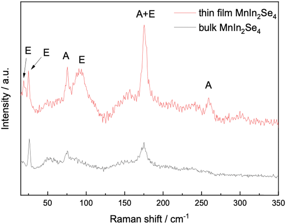 | ||
| Fig. 2 Raman spectra of bulk (black) and 2D (red) MnIn2Se4. | ||
The theoretical calculations for the identification of the Raman modes of MnIn2Se4 are in excellent agreement with the experimental data (Fig. S1, ESI†). The peaks at 75 and 259 cm−1 are the vibrational frequencies related to the A vibrational mode. The peak at 175 cm−1 contains both vibrational modes A and E. We also confirm that there are vibrational modes A with vibrational frequencies at 184.6, 238.7, 252.1, and 256.5 cm−1 with zero Raman intensity in the bulk phase. The phonon modes corresponding to the most prominent Raman peaks are presented in Fig. S2 (ESI†). These modes are grouped into five frequency ranges: 6.5, 21, 62, 86, and 165 cm−1. The angular orientations of the phonon modes within each group were analyzed. Phonon modes around 165 cm−1 are predominantly perpendicular to the 2D surface (5 out of 9 phonon modes). In contrast, those around 21 and 62 cm−1 are primarily parallel to the 2D surface (2 out of 6 phonon modes and 1 out of 3 phonon modes respectively). This observation aligns well with experimental results, which show a significant enhancement of the Raman peak near 165 cm−1 when transitioning from bulk to 2D, while the peaks around 26 and 75 cm−1 exhibit relatively minor intensity changes. However, we should mention that, as not all phonon modes within a given frequency range are strictly perpendicular or parallel to the 2D surface, it is not possible to categorize them exclusively into these two orientations. Nonetheless, all Raman peaks display varying degrees of intensity enhancement when transitioning from bulk to 2D.
The other Raman peaks are all assigned to the E phonon modes. As evident from the experimentally obtained data, upon exfoliation and reduction in the number of layers, in addition to the emergence of new peaks, the modes attributed to the A vibrational modes are amplified in intensity.
To further confirm the layered nature of the crystals synthesized via the CVT technique, their morphology was characterized by scanning electron microscopy coupled with energy dispersive spectroscopy (SEM/EDS). As displayed in Fig. 3, the SEM images represent the typical feature of layered materials, allowing us to identify the crystalline plane produced during the mechanical exfoliation. Furthermore, the EDS analysis revealed the homogenous distribution of the elements across the materials and an elemental quantification analysis in agreement with the expected stoichiometry of 1:2:4 for MnIn2Se4.
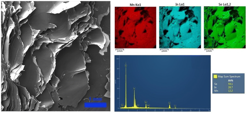 | ||
| Fig. 3 SEM image of a MnIn2Se4 crystal prepared via a CVT technique and the corresponding EDS elemental mapping, spectrum, and semi-quantitative analysis. | ||
Fig. 4 shows the STEM analyses performed on the MnIn2Se4 flakes. The size of the flakes is typically between 100 and 400 nm. The elemental quantification was extracted from the EDS analyses and is shown in Table S1 in the ESI.† The composition is in excellent agreement with the SEM/EDS analysis, as shown above, and corresponds to the expected stoichiometry. According to the EDS maps (Fig. 4(b)) as well as medium (Fig. S3, ESI†) and high-resolution STEM-HAADF images, the flakes appear homogeneous in composition. Fig. 4(d) shows the HR-STEM HAADF micrograph acquired on the same flake. The high-crystalline quality of the flake is clearly presented. The corresponding FFT pattern was successfully indexed, matching the MnIn2Se4R3m crystal structure, seen along the [0 0 1] zone axis. It should be noted that all the analyzed FFT and SAED patterns (Fig. S4, ESI†) were successfully indexed by using the expected crystal structure. All these results highlight the high-crystalline quality of the synthesized material.
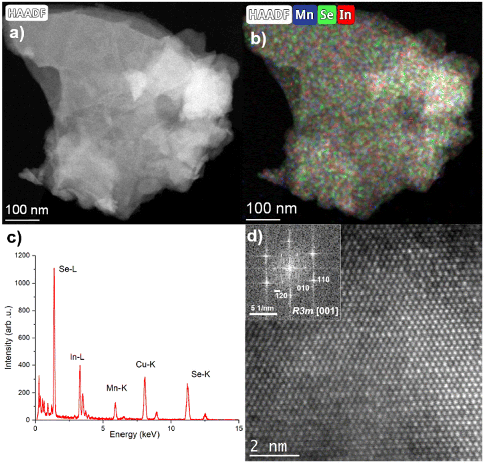 | ||
| Fig. 4 (a) Low magnification STEM-HAADF image of a MnIn2Se4 flake. (b) Corresponding Mn, Se, and In EDS maps, and (c) EDS spectrum extracted from the flake shown in (a). (d) HR-STEM HAADF image of the same flake. The inset displays the corresponding FFT pattern which has been successfully indexed with the MnIn2Se4R3m crystal structure seen along the [0 0 1] zone axis. | ||
Surface oxidation states were analyzed by X-ray photoelectron spectroscopy (XPS). The composition ratio calculated from the wide-survey spectrum was 1:2.05:3.78 (Fig. S5, ESI†) which is very close to the expected stoichiometry. Notably, the oxygen concentration was very low at ca. 3.8% showcasing good stability in ambient conditions. The core-level spectra of In 3d and Se 3d only displayed one oxidation state with energies similar to those reported previously.57 Furthermore, the high-resolution XPS spectrum of In 3d shows two clear, well-defined peaks corresponding to In 3d5/2 and 3d3/2 with a 7.54 eV spin–orbit separation (Fig. 5(b)), while lastly, the Se 3d high-resolution XPS peak was deconvoluted into Se 3d5/2 and Se 3d3/2 with a spin–orbit splitting of 0.86 eV, ascribed to Se−II (Fig. 5(c)). On the other hand, the spectrum of Mn 2p exhibited a much more complex structure (Fig. 5(a)). Previous studies on MnIn2Se4 in the literature show similar spectral features, where a broad main region from 639 eV to 645 eV is observed, accompanied by a strong satellite feature around 646 eV.57,58 In these studies, the presence of MnIII or MnIV is reported. However, extensive studies on Mn-based compounds (such as oxides, hydroxides, and oxides-hydroxides) suggest that a more complex multiplet fitting approach may be more suitable for Mn deconvolution. This complexity is reinforced by the fact that MnII, MnIII, and MnIV all exhibit similar binding energies which is in strong contrast to the aforementioned reports.59,60 Notably, only MnII species are commonly associated with satellite features, which aligns with the findings here.59 For Mn 2p deconvolution, we followed the procedure outlined in previous work,59 where the peak intensity ratios were adjusted slightly to obtain a satisfactory fit, acknowledging that values reported for Mn oxides may differ for other compounds. Due to the complexity of the deconvolution, these results should be considered to have qualitative significance at best and be interpreted with caution. The MnIn2Se4 flakes were ground and exfoliated by ultrasonication for 3 h with a programmed pulse of 2 s (En = 310 kJ) and DMF as a solvent. The suspension as prepared was analyzed by AFM (Fig. 6). The illustration of a representative AFM image of a MnIn2Se4 flake revealed a lateral size of 1.4 μm with a thickness of 30 nm. Further AFM images are shown in Fig. S6 (ESI†), where the thickness of the flakes varies between 20–50 nm and the lateral size between 1–1.6 μm.
 | ||
| Fig. 5 High-resolution XPS spectra of (a) Mn 2p, (b) In 3d, and (c) Se 3d regions. | ||
 | ||
| Fig. 6 AFM image and the corresponding height profile plotted for an exfoliated MnIn2Se4 flake. | ||
To investigate the light-harvesting properties of the as-prepared suspension, absorbance spectra of the MnIn2Se4 nanosheets in DMF were recorded. As shown in Fig. S7a (ESI†), the exfoliated MnIn2Se4 material presents a broad absorption profile in the visible range characterized by a peak around 450 nm, highlighting the possibility of obtaining an active photodetector system in the zone of blue light. The corresponding Tauc plot diagram (Fig. S7b, ESI†) locates the optical band gap at 1.88 eV. This value is close to those reported in the literature for bulk MnIn2Se4 semiconductor materials, which typically lie between 1.55 and 1.85 eV.49,50Fig. 7 shows a comparison of photoreflectance (PR), transmission (T), and photoacoustic (PA) spectra measured at room temperature for a 10 μm thick MnIn2Se4 crystal. The transparency region for this sample reaches ∼1.6 eV. Above this energy the PA spectrum saturates. Using the knee method for the PA spectrum,61,62 it is possible to determine the energy gap from the intersection of the saturated area and the PA signal growth area, see the intersection of the black lines. It is worth noting here that the absorption begins well below 1.6 eV, and this is clear from both transmission and photoacoustic measurements. In order to determine the nature of this absorption (indirect vs. direct), these spectra are compared with the photoreflectance spectrum, which is not sensitive to indirect absorption. This method probes only direct optical transitions at singularities of the total optical density of states.63 A distinct resonance is observed in the PR spectrum at 1.64 eV and is attributed to the direct band gap in MnIn2Se4. This resonance is modulated by a Fabry–Perot oscillation, which is strong in the transparency region and disappears above the transparency region. In order to extract the energy of the direct gap in MnIn2Se4, the PR spectrum is fitted (see the solid grey line) by the Aspnes formula64 (eqn (1))
 | (1) |
 | (2) |
 | ||
| Fig. 7 (a) Comparison of photoreflectance (green line), transmission (red line), and photoacoustic (blue line) spectra measured at room temperature. (b) Temperature dependence of absorption spectra. (c) Analysis of absorption spectra at low and room temperature. (d) Temperature dependence of indirect (open red diamonds) and direct (solid blue diamonds) gap determined from absorption measurements together with the direct gap determined at room temperature by photoacoustic spectroscopy (solid green triangle) and photoreflectance (solid cyan triangle). | ||
Thus, from this direct comparison of the PR spectrum with the transmission spectrum, it can be concluded that the fundamental energy gap in MnIn2Se4 is indirect. The conclusion is further supported by theoretical calculations which are presented in more detail below.
To determine the temperature dependence of the fundamental energy gap for MnIn2Se4, absorption measurements were carried out as a function of temperature, and the spectra are presented in Fig. 7(b). To determine the indirect gap, the square root of the absorption spectrum was drawn, where the linear dependence was extrapolated to zero and thus the indirect energy gap was determined. Additionally, the absorption square was plotted, and by linear extrapolation of this spectrum to zero the direct band gap was estimated (see the example analysis for determining the indirect and direct band gap in Fig. 7(c)). As can be seen, the direct energy gap determined in this way is ∼50 meV smaller than the energy gap determined using the photoreflectance method (compare the solid diamonds with the triangles in Fig. 7(d)). This difference is related to the non-parabolic nature of the valence band (note here that the linear relationship of the square of absorption used to determine the direct gap is expected for parabolic bands) and the sample thickness being too large to determine the direct band gap from absorption measurements.
Based on absorption measurements, it was found that the energy gap narrows with increasing temperature linearly with a factor of 0.39 ± 0.01 and 0.40 ± 0.01 μeV K−1 for the direct and indirect energy gap, respectively, see Fig. 7(d). This gives a narrowing of the gap by ∼110 meV in the temperature range of 20–320 K, which is slightly larger than that observed for group III–V semiconductors in the same temperature range (70–90 meV).65
As in other semiconductors, the narrowing of the energy gap with increasing temperature is associated with an increase in lattice parameters and electron–phonon interactions. Typically, the temperature dependence of the band gap is described using the empirical Varshni relationship66 (eqn (3)) or the Bose–Einstein formula67,68 (eqn (4)), which takes into account the electron–phonon interaction. The former relationship is given by:
 | (3) |
The latter formula, i.e., the Bose–Einstein one, can be written in the form of:
 | (4) |
 can be assumed for the Bose–Einstein relationship at T ≫ ΘB. Therefore, the linear fitting of the experimental results for direct and indirect energy gaps is justified in this case, especially since we expect a magnetic phase for this crystal at low temperatures. Hence, the expected nonlinearity in this temperature range can be suppressed. It has recently been shown that the energy gap for CrSBr in the antiferromagnetic and paramagnetic phases exhibits a slightly different temperature dependence69 and therefore the description of energy gap dependence by the simplest formula, i.e. linear approximation, may be the best solution in the first approximation.
Generally, MnIn2Se4 is a magnetic material due to the presence of Mn atoms, but the ferromagnetic phase is expected at very low temperatures. In our optical experiments, we are dealing with a paramagnetic phase, but this phase is a challenge in density functional theory (DFT) calculations. Therefore, we performed band structure calculations for the ferromagnetic phases using a hybrid functional (Fig. 8). So far, we have observed experimentally that the electronic structure (i.e., the energy gap, etc.) does not change much when the crystal goes from the magnetic to the paramagnetic phase.69 This means that calculations for the ferromagnetic phase can be used to interpret optical transitions observed for the paramagnetic phase. For the ferromagnetic phase of MnIn2Se4, it is clearly visible that we are dealing with a crystal with a fundamental indirect gap. A direct gap in this crystal is at the Γ point of BZ and is larger by ∼110 meV than the indirect gap. Therefore, we claim that our DFT calculations support experimental data on the indirect nature of the band gap in MnIn2Se4.
 | ||
| Fig. 8 Electronic band structure for the K–Γ–M path for ferromagnet MnIn2Se4 calculated with a PBE0 hybrid functional. | ||
2.1 Photoelectrochemical (PEC) photodetectors
Prior to the photoelectrochemical (PEC) experiments, the stability of the material was tested by submitting crystalline powder supported on a glassy carbon electrode (GCE) to potentials ranging from −0.1 to 1 V vs. SCE. As shown in Fig. 9(a), the material does not present any redox peak indicating the absence of any electrochemical reaction occurring in the specific potential window. | ||
| Fig. 9 (a) Cyclic voltammetry of MnIn2Se4 supported on a GCE. Scan rate 0.1 V s−1. (b) Linear sweep voltammetry of a MnIn2Se4/ITO electrode. | ||
20 μL of the exfoliated MnIn2Se4 DMF suspension was dropcast onto an ITO glass equipped with a mask which set the active area to a spot of 0.196 cm2. The electrodes were tested in a PEC cell equipped with a saturated calomel electrode (SCE) and platinum wire as the reference and counter electrodes, respectively. The scheme of the experimental setup employed in the PEC tests is represented in Fig. S8 (ESI†). The photoresponsive behavior of the MnIn2Se4/ITO electrode was studied by linear sweep voltammetry (LSV) as depicted in Fig. 9(b). The photodetector under illumination with chopped purple light (power 100 mW) shows a photoresponsive behavior in the range of 0.25–1 V vs. SCE.
A potential of 0.5 V vs. SCE was applied during the PEC tests to evaluate the photodetection performances of exfoliated MnIn2Se4 crystals supported on ITO toward LED light sources with wavelengths with frequencies spanning from the UV to the visible (purple light λ = 420 nm, blue light λ = 460 nm, green light λ = 532 nm, and red light λ = 633 nm). The chronoamperometric diagrams recorded with varying power of incident light are reported in Fig. 10.
 | ||
| Fig. 10 Power dependence of the photocurrent density under the illumination for a PEC-type MnIn2Se4/ITO photodetector upon irradiation with (a) UV (λ = 385 nm), (b) purple (λ = 420 nm), (d) blue (λ = 460 nm), (e) green light (λ = 532 nm), and (f) red light (λ = 633 nm) LED sources in 1 M KOH solution at 0.5 V vs. SCE. The power was set to the values of 50 mW (violet), 100 mW (olive), 200 mW (red), 300 mW (cyan), 500 mW (blue), 800 mW (green), and 1000 mW (black). (c) Response time of the PEC photodetector under the illumination with purple light LED with a power of 1000 mW. | ||
As displayed in Fig. 10(a)–(f), the chronoamperometry diagrams recorded with varying the intensity of the incident light show a trend characterized by a continuous increase in the photocurrent variation (Iph = Ilight − Idark) with the increase of the power, as a consequence of the increased number of photons promoting the creation of electron–hole pairs within the semiconductor material. A comparison of the results obtained performing the illumination under the wavelengths of 385, 420, 460, and 532 nm (herein named for simplicity UV, purple, blue, and green light) in the presence of 1 M KOH as the electrolyte demonstrates a predominant response to purple light and blue light which determine a maximum photocurrent density of 112.8 μA cm−2 and ∼59 μA cm−2 respectively (power 1000 mW).
Beyond blue light, the photodetector demonstrates a weak response to UV, green, and red light, reaching the photocurrent's values of ∼9.2, ∼4.1, and ∼2.3 μA cm−2, respectively.
The response time for purple light is represented in Fig. 10(c). The photodetector demonstrates a fast response toward the illumination being characterized by a delay of 0.1 s in reaching the maximum current density and a recovery time of 0.1 s to diminish the current to 20% of the value assumed under irradiation.
In order to further investigate the excited state characteristics of the bi-dimensional MnIn2Se4, transient absorption (TA) experiments were carried out. The transient absorption spectrum of MnIn2Se4 has been acquired at 500 ns upon illumination with a laser pulse at a 420 nm excitation wavelength (Fig. 11). The TA spectrum of a MnIn2Se4 dispersion in acetonitrile under a N2 atmosphere shows a continuous band decreasing in intensity from the UV towards the NIR. This is in consistent with the band gap value of MnIn2Se4 (reported in the range of 1.55 to 1.85 eV and measured as 1.88 eV).
 | ||
| Fig. 11 (a) Transient absorption spectrum of a N2-purged dispersion of MnIn2Se4 in acetonitrile, acquired at 500 ns upon 420 nm laser excitation. (b) Transient absorption decay of a N2-purged dispersion of MnIn2Se4 in acetonitrile, monitored at 360 nm upon 420 nm laser excitation. | ||
On the other hand, the transient decay of photogenerated species was monitored at 360 nm (Fig. 11(b)). The transient decay presents similar bimodal behavior in the range of ns–μs time scale, which can be fitted to a bi-exponential function (eqn (5)).
 | (5) |
The fitting of the experimental data obtained from MnIn2Se4 dispersions in acetonitrile under a N2 atmosphere and monitored at 360 nm shows a fast component of τ1 = 79 ns and a second component of τ2 = 553 ns. These results indicate the presence of two different types of defects acting as charge carrier traps which are most likely positioned deep within the bandgap.
To characterize the performances of the photodetector, figures of merit such as responsivity and photoresponse have been determined for the MnIn2Se4/ITO system. The responsivity describes the relationship between the photogenerated current per unity of area and the power density of the incident light, as expressed by eqn (6):
 | (6) |
 | (7) |
The responsivity and the photoresponse diagrams for the MnIn2Se4/ITO photodetector for the case of 1 M KOH as the electrolyte solution are reported in Fig. 12.
 | ||
| Fig. 12 (a) Responsivity and (b) photoresponse for the PEC-type MnIn2Se4/ITO photodetector in 1 M KOH solution at 0.5 V vs. SCE. | ||
The responsivity of the photodetector shows a trend identified by an exponential decrease of R in the increase with the power, owing to the higher fraction of electrons per unity of power that are promoted to the conduction band upon low-intensity illumination. Conversely, the responsivity diagram shows a minimum at high power values determined by a lower population of free charge carriers respective to the power of the incident light. In contrast, the photoresponse of the device demonstrates a steady growth concerning the power, which reflects the steady increase of the photogenerated current compared to the current under dark conditions.
The maximum values of responsivity and photoresponse are reached under purple and blue light irradiation, setting the maximum parameters for the MnIn2Se4/ITO photodetector to R = 8.41 mA W−1, PR = 2060 and R = 3.28 mA W−1, PR = 1070 respectively. The responsivity obtained under irradiation with UV, green, and red light demonstrates values an order of magnitude lower concerning purple and blue light pointing out a certain selectivity to the frequency in the range of 400 nm.
The values of responsivity obtained for MnIn2Se4/ITO can be compared with the results reported in the literature for PEC-type photodetectors performing in the presence of low applied potential (0–1 V). As shown in Table 1, the values obtained in the present work for the MnIn2Se4/ITO photodetector exceed those reported for other layered mono- and ternary-sulfides reaching the values obtained for perovskite-based heterojunction systems.
| Material(s) | Device configuration | Electrolyte | Applied potential (V) | Responsivity (mA W−1) | Wavelength (nm) | Ref. |
|---|---|---|---|---|---|---|
| ZnIn2S4–Ag. Gel-Pt | Metal–semiconductor–metal | — | 0 | 0.02 | Simulated sunlight | 70 |
| InSe nanosheets | PEC-type | 0.2 M KOH | 1 | 3.3 × 10⁻³ | 455 | 71 |
| 4.0 × 10⁻³ | ||||||
| Black phosphorous nanosheets | PEC-type | 0.1 M KOH | 0 | 1.9 × 10⁻³ | Simulated sunlight | 72 |
| 2.2 × 10⁻³ | ||||||
| GeSe nanosheets | PEC-type | 0.1 M KOH | 0.3 | 0.044 | Simulated sunlight | 73 |
| 0.076 | ||||||
| SnS | PEC-type | 0.1 M Na2SO4 | 0.6 | 0.018 | 365 | 74 |
| Perovskite (CH3NH3PbI3) | Metal–semiconductor–metal | — | 5 | 4.4 | 633 | 75 |
| Perovskite (CH3NH3PbI3) PDPP3T | Metal–semiconductor–metal | — | 1 | 10.7 | 365 | 76 |
| 25.5 | 650 | |||||
| 5.5 | 937 | |||||
| MnIn2Se4 | PEC-type | 1 M KOH | 0.5 | 8.41 | 420 | This work |
Furthermore, detectivity (D*) is another crucial parameter that quantifies the efficiency of a photodetector in detecting weak optical signals. It is expressed in eqn (8):
 | (8) |
 | (9) |
 | ||
| Fig. 13 Detectivity (D*) of the MnIn2Se4 photodetector across various wavelengths. | ||
3. Conclusion
To summarize, the properties of MnIn2Se4, a novel layered, ternary material, have been thoroughly characterized with respect to its structure, morphology, and optics using a combination of experimental results and DFT calculations. In this manuscript, we report the indirect nature of the material's bandgap and additionally, the material has been studied as a photodetector in an alkaline environment where it showed excellent response upon blue and purple irradiation with a photocurrent density maximum of 59 and 112.8 μA cm−2 respectively. The responsivity of the material at these wavelengths was found to be higher than that of similarly reported devices with values at 8.41 and 3.28 mA W−1 for 420 and 460 nm wavelength illumination. Based on these results, the investigation of the usage of ternary chalcogenides as photodetectors is highly anticipated.4. Experimental section
4.1 MnIn2Se4 synthesis
MnIn2Se4 crystals were prepared by chemical vapor transport (CVT) in a quartz glass ampoule. Manganese (99.95%, −100 mesh, Mateck), indium (99.9999%, 1–2 mm, Wuhan Xinrong New Material Co., China) and selenium (99.9999%, 2–4 mm, Wuhan Xinrong New Material Co., China) were placed in quartz ampoule (35 × 180 mm, wall thickness 3 mm) in amounts corresponding to 20 g of MnIn2Se4 together with 0.5 g of iodine (99.9%, granules, Fisher Scientific, USA) and melt sealed under high vacuum (under 10−3 Pa, diffusion pump with LN2 trap). The ampoule was first placed in a muffle furnace and heated at 500 °C for 25 h, at 600 °C for 50 hours and at 800 °C for 50 hours. After the reaction in a muffle furnace, the ampoule was placed in a horizontal two-zone furnace for CVT crystal growth. First, the growth zone was heated at 850 °C and the source zone at 600 °C. After two days, it was thermal gradient reversed and the crystal growth took 10 days (source zone at 850 °C and growth zone at 750 °C). After growth, the ampoule was opened in an argon-filled glovebox.Solvent-assisted exfoliation was performed in DMF by ultrasonication. First, the CVT growth crystals were ground in an agate mortar and sieved. Subsequently, ultrasonication was performed in DMF (1 mg mL−1) using a 100 W sonotrode under an argon atmosphere (Bandeline Sonoplus HD2200).
4.2 Material characterization techniques
XRD patterns were acquired on a Bruker D8 Discover powder diffractometer (Bruker, Germany) in Bragg–Brentano parafocusing geometry with Cu Kα radiation, in an angular range of 5–90° 2θ, with a step size of 0.020° and the data was analyzed with HighScore Plus 3.0e software. The Raman spectrum were obtained using an inVia Raman microscope (Renishaw, England) in backscattering geometry with a CCD detector for Raman spectroscopy. DPSS laser (532 nm, 50 mW) with an applied power of 5 mW and 50× magnification objective was used for the measurement. Instrument calibration was achieved with a silicon reference which gives a peak position at 520 cm−1 and a resolution of less than 1 cm−1. The samples were suspended in deionized water (1 mg mL−1) and ultrasonicated for 10 min. The suspension was deposited on a small piece of silicon wafer and dried.The morphology was investigated using SEM with a FEG electron source (Tescan Lyra dual beam microscope). Elemental composition and mapping were performed using an EDS analyzer (X-MaxN) with a 20 mm2 SDD detector (Oxford instruments) and AZtecEnergy software. To conduct the measurements, the samples were placed on carbon conductive tape. SEM and EDS measurements were carried out using a 10 kV electron beam. The STEM was performed with a Tescan Lyra dual beam microscope equipped with an FEG electron source and STEM sample holder. To conduct the measurements, the sample suspension was dropcast onto a 200 mesh Cu TEM grid and dried in a vacuum oven (50 °C). STEM measurements were carried out using a 30 kV electron beam.
Aberration-corrected high-resolution (scanning) transmission electron microscopy imaging (HR-(S)TEM) and energy-dispersive X-ray spectroscopy (EDS) were performed using a FEI Titan Cubed Themis microscope (University of Cádiz), which was operated at 80 kV. It is equipped with a double Cs aberration-corrector, a monochromator, an X-FEG gun, an ultrahigh-resolution energy filter (Gatan Quantum ERS), which allows working in dual-EELS mode, and a super-X EDS detector, which consists of four windowless SDD detectors that can be read out independently. HR-STEM imaging was performed using a high-angle annular dark-field (HAADF) detector. EDS quantification was achieved using the Brown–Powell model for the ionization cross sections. Selected Area Electron Diffraction (SAED) and fast Fourier transform (FFT) patterns were automatically indexed using the JEMS software.77
High-resolution XPS was performed using an ESCAProbeP spectrometer (Omicron Nanotechnology Ltd, Germany) with a monochromatic aluminum X-ray radiation source (1486.7 eV). Wide-scan surveys of all elements were performed, with subsequent high-resolution scans of manganese (Mn 2p), indium (In 3d), and selenium (Se 3d). Relative sensitivity factors were used to evaluate the carbon-to-oxygen (C/O) ratios from the survey spectra. The samples were placed on a conductive carrier made from a high-purity silver bar. An electron gun was used to eliminate sample charging during measurement (1–5 V). All XPS spectra were analyzed by CasaXPS software.
AFM observations were implemented using a Ntegra Spectra from NT-MDT. The surface scans were carried out in a tapping (semi-contact) mode. Cantilevers with a strain constant of 1.5 kN m−1 equipped with a standard Si tip with a curvature radius lower than 10 nm were used for the measurements. The AFM imaging was performed by drop-casting a sample suspension (1 mg mL−1) on freshly cleaved mica substrate. The measurements were conducted in ambient conditions with a scan rate of 1 Hz and scan line of 512. Data analysis was done using the software package Gwyddion.
4.3 Electrochemistry
The electrochemical characterization by means of cyclic voltammetry was performed using an Autolab PGSTAT 204 (Metroohm, Switzerland). All glassy carbon electrodes were cleaned by polishing with an alumina suspension to renew the electrode surface then washed and wiped dry prior to any use. For the measurement a modified glass carbon electrode was used as a working electrode, with a calomel reference electrode, and a platinum counter electrode.ITO electrodes were cleaned by rinsing with water, ethanol, and acetone and dried at 60 °C. An adhesive mask was applied to reduce the active area to a circle of 0.5 cm in diameter. The samples were dispersed in DMF as the organic solvent to obtain a 1 mg mL−1 suspension. The suspension was then sonicated for 5 min at room temperature before every use. A cleaned ITO electrode was then modified by coating with a 10 μL aliquot of the suspension and left to dry in a box oven at 60 °C to prepare MnIn2Se4/ITO electrodes. The modified GC electrodes, SCE reference electrode, and platinum counter electrode were then placed into an electrochemical cell which contains the electrolyte solution, and the measurements were then taken. All measurements were performed for three consecutive scans at a scan rate of 100 mV s−1.
4.4 Optical measurements
For photoreflectance measurements, the sample was illuminated with a spectrum of white light from a halogen lamp, which, after being reflected from the sample, was directed at a monochromator (Triax 550) using appropriate lenses. The dispersed light was analyzed step by step (wavelength by wavelength) by measuring its intensity using a silicon photodiode. A 405 nm laser with a power of 80 mW was used to modulate the surface electric field in the sample. The laser beam was modulated at a frequency of 280 Hz. Changes in the reflection (ΔR) caused by laser modulation were measured in the lock-in technique using a phase-sensitive nanovoltmeter (Stanford SR830). The reflectance spectrum (R) was simultaneously measured to obtain the photoreflectance spectrum, i.e., ΔR/R. The spot size of the probing beam (white light) and the size of the laser beam on the sample were very comparable and had a diameter of 1–2 mm. For more details of photoreflectance measurements see ref. 63.For photoacoustic measurements, the sample was placed in a photoacoustic chamber equipped with a broadband microphone.78 The sample was illuminated with monochromatic light from a halogen lamp after passing through a monochromator (iHR 320). The measurements were performed using the lock-in technique with a phase-sensitive nanovoltmeter (Stanford SR830) and modulating the light beam with a frequency of 20 Hz. Powdered carbon was used to calibrate the system.
For transmission (absorption) measurements at various temperatures, the sample was placed in a closed-cycle helium-cooled cryostat, which allows measurements in the temperature range from 10 to 325 K. The light from the halogen lamp, after passing through the monochromator (Omni-λ300i), was directed at the sample, and after passing through the sample, at the silicon (and InGaAs) photodiode. The light beam was modulated in front of the monochromator at a frequency of 280 Hz and its transmission through the sample was measured in the lock-in technique with a Stanford SR830 phase-sensitive nanovoltmeter.
4.5 DFT calculations
The electronic structure and Raman spectra of MnIn2Se4 were computed by density functional theory (DFT) calculations using two codes: Quantum ESPRESSO code79,80 together with norm-conserving SG15 pseudopotentials81,82 and Vienna Ab Initio Simulation Package together with the PAW method.83–86 In the first approach, we calculated the Raman spectrum using the Perdew, Burke, and Ernzerhof (PBE) exchange–correlation functional.87 The cut-off energies of the wave function and charge density were chosen to be 70 Ry and 280 Ry respectively. All structures are relaxed until the force is less than 5.0 × 10⁻⁴ Ryd Bohr−1. We used an 8 × 8 × 1 k-mesh for surface structure calculation and Γ-point only for molecular structure calculations. Electronic spin-polarization is also considered in all the simulations, and we verified that for the bulk MnIn2Se4 structure, the ferromagnetic structure has a 1.47 eV lower energy per manganese atom than the anti-ferromagnetic ordering. Thus, we assumed a ferromagnetic state in all the following calculations. To overcome the lack of van der Waals interactions in the PBE functional, the semiempirical Grimme's DFT-D3 correction88 is applied. The resulting exfoliation energy is 13.54 meV Å−2, which also indicates that bulk MnIn2Se4 is easy to exfoliate and confirms its potential application as a low-dimensional material.89As the PBE level of DFT predicts no band gap for bulk MnIn2Se4 a Hubbard U correction is applied,90 which improves the PBE electronic structure and correctly predicts the semiconducting nature of the material. In the MnIn2Se4 structure shown in Fig. S10 (ESI†), selenium atoms are divided into two types, namely the Se-outer and Se-inner. The outer selenium atoms only have chemical bonds with indium atoms and are placed on the outer side of the MnIn2Se4 layer. The inner selenium atoms have both chemical bonds with manganese atoms and indium atoms and are placed inside the MnIn2Se4 layer. In our treatment, we consider these two types of selenium atoms as different types. We therefore calculated from first-principles the U values by using the HP module of Quantum ESPRESSO, which uses density-functional perturbation theory to calculate the constrained linear-response matrices employed in the prediction of the Hubbard U parameters.91,92 All the U-values are calculated using a 2 × 2 × 1 q-mesh and are obtained from a single calculation, meaning no self-consistent procedure convergence of the Hubbard parameters was applied. The ortho-atomic manifolds were used in all the Hubbard calculations as orbital projectors.93 We obtain 5.06 eV for the manganese 3d orbital, 3.34 eV for the inner selenium 4p orbital, and 3.11 eV for the outer selenium 4p orbital. For indium atoms, as the 4d orbital is very close–shell, the occupation number on the 4d-orbital is not going to change significantly when a perturbation is performed. As a consequence, we do not apply any Hubbard correction to the 4d orbital of indium atoms. An 8 × 8 × 1 k-points mesh is used in all self-consistent electronic calculations and linear response Hubbard-U calculations.
The Raman spectra were computed by the AiiDA-vibroscopy package,94 which uses the AiiDA95–97 interactive infrastructure to automatically submit jobs on remote machines, while managing data and workflows locally. We used the finite electric field98,99 and the finite displacement100 methods to carry out the calculation of the Raman tensors and force constants matrix needed for the prediction of the Raman spectra. These techniques allow for the usage of any functional, hence are suitable for considering the Hubbard corrections. The Raman spectra were computed considering a powder phase, a 532 nm incoming laser wavelength, and a temperature of 300 K. Since experimental Raman spectra are acquired at room temperature, the material is found in a paramagnetic state, with zero total magnetization. For the Raman calculations only, we model the magnetic state of the bulk in an anti-ferromagnetic configuration, which can be considered as a very first approximation of paramagnetic ordering. The simple anti-ferromagnetic structure is found to be sufficient to reach good agreement with experimental data (Fig. S1, ESI†), thus is sufficient to carry out normal mode analysis in this material.
Apart from the calculation at the DFT+U level, we also performed band structure calculations by means of a hybrid functional via the VASP code, with the aim of obtaining better quantitative agreement with the experimental band gap. For geometry optimization, we used, as in the Quantum ESPRESSO simulations, the PBE functional together with D3 corrections. The resulting lattice constants a = 4.045 Å and c = 39.718 Å are in good agreement with the experiments (4.057 and 39.497 Å). The refined calculation of electronic properties was carried out by employing the PBE0 hybrid functional. In order to further improve agreement with optical measurements we fitted parameters that mix GGA and HF exchange in the PBE0 functional in such a way as to achieve an experimental direct band gap. The final mixing parameter was fixed at 0.33 (for PBE0 it is 0.25). All calculations were performed with an energy cutoff of 600 eV and k-point sampling of 10 × 10 × 1.
Data availability
The datasets generated during and/or analyzed during the study are accessible via the Zenodo repository: https://doi.org/10.5281/zenodo.13827444.Conflicts of interest
The authors declare no conflicts of interest.Acknowledgements
Z. S. was supported by the ERC-CZ program (project LL2101) from the Ministry of Education Youth and Sports (MEYS). We acknowledge funding from the European Union through the 2D-PRINTABLE project (GA-101135196). This work was supported by the project “The Energy Conversion and Storage” funded as project no. CZ.02.01.01/00/22_008/0004617 by Programme Johannes Amos Commenius, call Excellent Research. N. A. acknowledges funding from the National Science Centre (NCN) Poland SONATA 19 Grant no. 2023/51/D/ST11/02588 and at Wrocław University of Science and Technology, and this work was supported by the National Science Centre (NCN) Poland OPUS 23 no. 2022/45/B/ST7/02750. Calculations have been carried out using resources provided by Wrocław Centre for Networking and Supercomputing. L. L. acknowledges funding from the Spanish Ministerio de Economía y Competitividad, the Ministerio de Ciencia e Innovación MCIN/AEI/10.13039/501100011033/FEDER UE, and the European Union “NextGenerationEU”/PRTR (PID2022-140370NB-I00, RYC2021-033764-I, CPP2021-008986). The (S)TEM measurements were performed at the National Facility ELECMI ICTS (“Division de Microscopia Electronica”, Universidad de Cadiz, DME-UCA). Financial support by the Spanish Ministry of Science and Innovation (CEX-2021-001230-S and PDI2021-0126071-OB-CO21 funded by MCIN/AEI/10.13039/501100011033) and Generalitat Valenciana (Prometeo 2021/038 and Advanced Materials programme Graphica MFA/2022/023 with funding from European Union NextGenerationEU PRTR-C17.I1). J. A. thanks the Spanish Ministry of Science and Innovation for a Ramon y Cajal research associate contract (RYC2021-031006-I financed support by MCIN/AEI/10.13039/501100011033 and by European Union/NextGenerationEU/PRTR). L. B. and N. M. gratefully acknowledge support from the Deutsche Forschungsgemeinschaft (DFG) under Germany's Excellence Strategy (EXC 2077, no. 390741603, University Allowance, University of Bremen) and Lucio Colombi Ciacchi, the host of the “U Bremen ExcellenceChair Program”. N. M. acknowledges support by the NCCR MARVEL, a National Centre of Competence in Research, funded by the Swiss National Science Foundation (grant number 205602). K. J. S. was supported by the Johannes Amos Comenius Programme, European Structural and Investment Funds, project CHEMFELLS VI (no. CZ.02.01.01/00/22_010/0008122).References
- (a) Y. Li, Z. Li, C. Chi, H. Shan, L. Zheng and Z. Fang, Adv. Sci., 2017, 4, 1600430 CrossRef PubMed; (b) Z. Li, E. Hong, X. Zhang, M. Deng and X. Fang, Small, 2023, 19, 2206310 CrossRef PubMed; (c) X. Fan, E. Hong, P. Wang and X. Fang, Adv. Mater., 2024, 36, 2400365 CrossRef PubMed; (d) Z. Li, E. Hong, X. Zhang, M. Deng and X. Fang, J. Phys. Chem. Lett., 2022, 13, 1215 CrossRef CAS PubMed; (e) M. Deng, Z. Li, S. Liu, X. Fang and L. Wu, Nat. Commun., 2024, 15, 8789 CrossRef CAS PubMed.
- I. Choudhuri, P. Bhaurival and B. Pathak, Chem. Mater., 2019, 31, 8260 CrossRef CAS.
- Y. Zhu, L. Peng, Z. Fang, C. Yan, X. Zhang and G. Yu, Adv. Mater., 2018, 30, 1706347 CrossRef PubMed.
- J. Park, M. S. Kim, E. Cha, J. Kim and W. Choi, Sci. Rep., 2017, 7, 16121 CrossRef PubMed.
- D. L. Duong, S. J. Yun and Y. H. Lee, ACS Nano, 2017, 11, 11803 CrossRef CAS PubMed.
- N. Perea-López, A. L. Elías, A. Barkdemir, A. Castro-Beltrán, H. R. Gutiérrez, S. Feng, R. Lv, T. Hayashi, F. López-Urías, S. Ghosh, B. Muchharla, S. Talapatra and H. Terrones, Adv. Funct. Mater., 2013, 23, 5511 CrossRef.
- C. Cong, J. Shang, Y. Wang and T. Yu, Adv. Opt. Mater., 2017, 6, 1700767 CrossRef.
- J. Li, J. Han, H. Li, X. Fan and K. Huang, Mater. Sci. Semicond. Process., 2020, 107, 104804 CrossRef CAS.
- N. Huo, J. Kang, Z. Wei, S.-S. Li, J. Li and S.-H. Wei, Adv. Funct. Mater., 2014, 24, 7025 CrossRef CAS.
- G. A. Muller, J. B. Cook, H.-S. Kim, S. H. Tolbert and B. Dunn, Nano Lett., 2015, 15, 1911 CrossRef CAS PubMed.
- Z. Zhang, Y. Ouyang, Y. Cheng, J. Chen, N. Li and G. Zhang, Phys. Rep., 2020, 860, 1 CrossRef CAS.
- D. Bhattacharya, S. Mukherjee, R. K. Mitra and S. K. Ray, Nanotechnology, 2020, 31, 145701 CrossRef CAS PubMed.
- M. Singh, E. D. Gaspera, T. Ahmed, S. Walia, R. Ramanathan, J. van Embden, E. Mayes and V. Bansal, 2D Mater., 2017, 4, 025110 CrossRef.
- A. Ciarrocchi, A. Avsar, D. Ovchinikov and A. Kis, Nat. Commun., 2018, 9, 919 CrossRef PubMed.
- S. Lei, L. Ge, Z. Liu, S. Najmaei, G. Shi, G. You, J. Lou, R. Vajtai and P. M. Ajayan, Nano Lett., 2013, 13, 2777–2781 CrossRef CAS PubMed.
- J. D. Yao, Z. Q. Zheng, J. M. Shao and G. W. Yang, Nanoscale, 2015, 7, 14974–14981 RSC.
- W. Huang, L. Gan, H. Yang, N. Zhou, R. Wang, W. Wu, H. Li, Y. Ma, H. Zeng and T. Zhai, Adv. Funct. Mater., 2017, 27, 1702448 CrossRef.
- L. Wang, P. Hu, Y. Long, Z. Liu and X. He, J. Mater. Chem. A, 2017, 5, 22855 RSC.
- T. Gao, Q. Zhang, L. Li, X. Zhou, L. Li, H. Li and T. Zhai, Adv. Opt. Mater., 2018, 6, 1800058 CrossRef.
- P. Yu, J. Lin, L. Sun, Q. L. Le, X. Yu, G. Gao, C.-H. Hsu, D. Wu, T.-R. Chang, Q. Zeng, F. Li, Q. J. Wang, H.-T. Jeng, H. Lin, A. Trampert, Z. Shen, K. Suenaga and Z. Liu, Adv. Mater., 2017, 29, 1603991 CrossRef PubMed.
- T. Maeda, W. Gong and T. Wada, Jpn. J. Appl. Phys., 2016, 55, 04ES15 CrossRef.
- V. Kiran, D. Mukherjee, R. N. Jenjeti and S. Sampath, Nanoscale, 2014, 6, 12856 RSC.
- J. Shi, T. F. T. Cerqueira, W. Cui, F. Nogueira, S. Botti and M. A. L. Marques, Sci. Rep., 2017, 7, 43179 CrossRef PubMed.
- K. Pal, Y. Xia, J. Shen, J. He, Y. Luo, M. G. Kanatzidis and C. Wolverton, npj Comput. Mater., 2021, 7, 82 CrossRef CAS.
- H. Haeuseler, J. Solid State Chem., 1979, 29, 121 CrossRef CAS.
- C. Razzetti, P. P. Lottici and G. Antonioli, Prog. Cryst. Growth Charact., 1987, 15, 43 CrossRef.
- K.-J. Ranged, Z. Naturforsch., 1996, 51b, 1363 CrossRef.
- S. A. Lopez-Rivera, A. J. Mora, D. Acosta Najarro, A. V. Rivera and R. Avila Godoy, Semicond. Sci. Technol., 2001, 16, 367 CrossRef CAS.
- C. Rincón, Phys. Rev. B: Condens. Matter Mater. Phys., 1992, 45, 12716 CrossRef PubMed.
- L. Gastaldi, A. Maltese and S. Viticoli, J. Cryst. Growth, 1984, 66, 673 CrossRef CAS.
- G. Döll, M. C. Lux-Steiner, C. Kloc, J. R. Baumann and E. Bucher, J. Cryst. Growth, 1990, 104, 593 CrossRef.
- T. Ohtani, H. Honjo and H. Wada, Mater. Res. Bull., 1987, 22, 829 CrossRef CAS.
- F. J. Manjon, I. Tiginyanu and V. Ursaki, Pressure-Induced Phase Transitions in AB2X4 Chalcogenide Compounds, Springer Series in Material Science, Springer, Berlin, Heidelberg, 2014 Search PubMed.
- S.-H. Wei, L. G. Ferreira and A. Zunger, Phys. Rev. B: Condens. Matter Mater. Phys., 1992, 45, 2533(R) CrossRef PubMed.
- J. Yang, J. Wang, C. Yang, W. Zhang and S.-H. Wei, Phys. Rev. Mater., 2020, 4, 085402 CrossRef CAS.
- G. Zhang, H. Wu, D. Chen, N. Li, Q. Xu, H. Li, J. He and J. Lu, Green Energy Environ., 2021, 7, 176 CrossRef.
- J. Wang, S. Sun, R. Zhou, Y. Li, Z. He, H. Ding, D. Chen and W. Ao., J. Mater. Sci. Technol., 2021, 78(1) Search PubMed.
- L. Shi, P. Yin and Y. Dai, Langmuir, 2013, 29, 12818 CrossRef CAS PubMed.
- T. Liu, L. Wang, X. Liu, C. Sun, Y. Lv, R. Miao and X. Wang, J. Chem. Eng., 2020, 379, 122379 CrossRef CAS.
- Z. Lei, W. You, M. Liu, G. Zhou, T. Takata, M. Hara, K. Domen and C. Li, Chem. Commun., 2003, 2142 RSC.
- F. Xing, Q. Liu and C. Huang, Sol. RRL, 2020, 4, 1900483 CrossRef CAS.
- X. Jiao, Z. Chen, X. Li, Y. Sun, S. Gao, W. Yan, C. Wang, Q. Zhang, Y. Lin, Y. Luo and Y. Xie, J. Am. Chem. Soc., 2017, 139, 7586 CrossRef CAS PubMed.
- S. Wang, B. Y. Guan, Y. Lu and X. W. “D.” Lou, J. Am. Chem. Soc., 2017, 139, 17305 CrossRef CAS PubMed.
- L. Guo, X. Han, K. Zhang, Q. Zhao, D. Wang and F. Fu, Catalysts, 2019, 9, 729 CrossRef CAS.
- M. Hao, X. Deng, L. Xu and Z. Li, Appl. Catal., B, 2019, 252, 18 CrossRef CAS.
- L. Valdman, V. Mazánek, P. Marvan, M. Serra, R. Arenal and Z. Sofer, Adv. Opt. Mater., 2021, 8, 2100845 CrossRef.
- J. Wei, C. Wang, T. Zhang, C.-M. Dai and S. Chen, Nanoscale, 2019, 11, 13924 RSC.
- N. N. Niftiev, M. A. Alidzhanov, O. B. Tagiev, F. M. Mamedov and M. B. Muradov, Semiconductors, 2004, 38, 531 CrossRef CAS.
- J. Choi, S. Choi, J. Choi, Y. H. Hwang, Y. H. Um, S. C. Hong and S. Cho, J. Korean Phys. Soc., 2004, 45, 672 CAS.
- C. Rincón, T. E. Torres, V. Sagredo, S. J. Jiménez-Sandoval and E. Mares-Jacinto, Phys. B, 2015, 477, 123 CrossRef.
- J. C. Mantilla Ochoa, V. Bindilatti, E. ter Haar, J. A. H. Coaquira, G. E. de Souza Brito, X. Gratens and V. Sagredo, J. Magn. Magn. Mater., 2004, 272–276, 1308 CrossRef.
- F. Chen, H. Huang, L. Guo, Y. Zhang and T. Ma, Angew. Chem., Int. Ed., 2019, 58, 10061 CrossRef CAS PubMed.
- J. Li, L. Cai, J. Shang, Y. Yu and L. Zhang, Adv. Mater., 2016, 18, 4059 CrossRef PubMed.
- H. Liang, T. Feng, S. Tin, K. Zhao, W. Wang, B. Dong and L. Cao, Chem. Commun., 2019, 55, 15061 RSC.
- D. Zhang, D. Chao, C. Yu, Q. Zhu, S. Zhou, L. Tian and L. Zhou, J. Phys. Chem. Lett., 2021, 12, 8939 CrossRef CAS PubMed.
- G. Enlai, L. Shao-Zhen, Q. Zhao, M. J. Buehler, F. Xi-Qiao and X. Zhiping, J. Mech. Phys. Solids, 2018, 115, 248 Search PubMed.
- J. Yang, Z. Zhou, J. Fang, H. Wen, Z. Lou, G. Shen and Z. Wei, Appl. Phys. Lett., 2019, 115, 222101 CrossRef.
- H. Sun, H. Liang, Q. Xu, F. Zhou and L. Cao, Catal. Lett., 2024, 154, 2551 CrossRef CAS.
- M. C. Biesinger, B. P. Payne, A. P. Grosvenor, L. W. M. Lau, A. R. Gerson and R. S. C. Smart, Appl. Surf. Sci., 2011, 257, 2717 CrossRef CAS.
- H. W. Nesbitt and D. Banerjee, Am. Mineral., 1998, 83, 305 CrossRef CAS.
- A. K. Bhatnagar and S. V. Subrahmanyam, Solid State Commun., 1982, 42, 281 CrossRef CAS.
- J. J. Prias-Barragan, L. Tirado-Mejia, H. Ariza-Calderon, L. Banos, J. J. Perez-Bueno and M. E. Rodriguez, J. Cryst. Growth, 2006, 286, 279 CrossRef CAS.
- R. Kudrawiec and W. Walukiewicz, J. Appl. Phys., 2019, 126, 141102 CrossRef.
- D. E. Aspnes, Surf. Sci., 1973, 37, 418 CrossRef CAS.
- I. Vurgaftman, J. R. Meyer and L. R. Ram-Mohan, J. Appl. Phys., 2001, 89, 5815 CrossRef CAS.
- Y. P. Varshni, Physica, 1967, 34, 149–154 CrossRef CAS.
- S. Logothetidis, M. Cardona, P. Lautenschlager and M. Garriga, Phys. Rev. B: Condens. Matter Mater. Phys., 1986, 34, 2458–2469 CrossRef CAS PubMed.
- P. Lautenschlager, M. Garriga, S. Logothetidis and M. Cardona., Phys. Rev. B: Condens. Matter Mater. Phys., 1987, 35, 9174–9189 CrossRef CAS PubMed.
- W. M. Linhart, M. Rybak, M. Birowska, P. Scharoch, K. Mosina, V. Mazánek, D. Kaczorowski, Z. Sofer and R. Kudrawiec, J. Mater. Chem. C, 2023, 11, 8423 RSC.
- L. Mandal, N. S. Chaudhri and S. Ogale, ACS Appl. Mater. Interfaces, 2013, 5, 9141 CrossRef CAS PubMed.
- Z. Li, H. Qiao, Z. Guo, X. Ren, Z. Huang, X. Qi, S. C. Dhanabalan, J. S. Ponraj, D. Zhang, J. Li, J. Zhao, J. Zhong and H. Zhang, Adv. Funct. Mater., 2017, 28, 1705237 CrossRef.
- X. Ren, Z. Li, Z. Huang, D. Sang, H. Qiao, X. Qi, J. Li, J. Zhong and H. Zhang, Adv. Funct. Mater., 2017, 27, 1606834 CrossRef.
- D. Ma, J. Zhao, R. Wang, C. Xing, Z. Li, W. Huang, X. Jiang, Z. Guo, Z. Luo, Y. Li, J. Li, S. Luo, Y. Zhang and H. Zhang, ACS Appl. Mater. Interfaces, 2019, 11, 4278 CrossRef CAS PubMed.
- W. Huang, Z. Xie, T. Fan, J. Li, Y. Wang, L. Wu, D. Ma, Z. Li, Y. Ge, Z. N. Huang, X. Dai, Y. Xiang, J. Li, X. Zhu and H. Zhang, J. Mater. Chem. C, 2018, 6, 9582 RSC.
- H. Fang, J. Li, J. Ding, Y. Sun, Q. Li, J.-L. Sun, L. Wang and Q. Yan, ACS Appl. Mater. Interfaces, 2017, 9, 10921 CrossRef CAS PubMed.
- S. Chen, C. Teng, M. Zhang, Y. Li, D. Xie and G. Shi, Adv. Mater., 2016, 28, 5969 CrossRef CAS PubMed.
- P. Stadelmann, JEMS Java Electron Microscopy Software, 2014, https://www.jems-swiss.ch/ Search PubMed.
- S. J. Zelewski and R. Kudrawiec, Sci. Rep., 2017, 7, 15365 CrossRef PubMed.
- P. Giannozzi, S. Baroni, N. Bonini, M. Calandra, R. Car, C. Cavazzoni, D. Ceresoli, G. L. Chiarotti, M. Cococcioni, I. Dabo, A. Dal Corso, S. de Gironcoli, S. Fabris, G. Fratesi, R. Gebauer, U. Gerstmann, C. Gougoussis, A. Kokalj, M. Lazzeri, L. Martin-Santos, N. Marzari, F. Mauri, R. Mazzarello, S. Paolini, A. Pasquarello, L. Paulatto, C. Sbraccia, P. Umari and R. M. Wentzcovitch, J. Phys.: Condens. Matter, 2009, 21, 395502 CrossRef PubMed.
- P. Gianozzi, O. Andreussi, T. Brumme, O. Bunau, M. Buongiorno Nardelli, M. Calandra, R. Car, C. Cavazzoni, D. Ceresoli, M. Cococcioni, N. Colonna, I. Carnimeo, A. Dal Corso, S. de Gironcoli, P. Delugas, R. A. DiStasio Jr., A. Ferretti, A. Floris, G. Fratesi, G. Fugallo, R. Gebauer, U. Gerstmann, F. Giustino, T. Gorni, J. Jia, M. Kawamura, H.-Y. Ko, A. Kokal, E. Küçükbenli, M. Lazzeri, M. Marsili, N. Marzari, F. Mauri, N. L. Nguyen, H.-V. Nguyen, A. Otero-de-la-Roza, L. Paulatto, S. Poncé, D. Rocca, R. Sabatini, B. Santra, M. Schlimpf, A. P. Seitsonen, A. Smogunov, I. Timrov, T. Thornhauser, P. Umari, N. Vast, X. Wu and S. Baroni, J. Phys.: Condens. Matter., 2017, 29, 465901 CrossRef PubMed.
- D. R. Hamann, Phys. Rev. B, 2017, 95, 239906 CrossRef.
- M. Schlimpf and F. Gygi, Comput. Phys. Commun., 2015, 196, 36 CrossRef.
- G. Kresse and J. Hafner, Phys. Rev. B: Condens. Matter Mater. Phys., 1993, 47, 558(R) CrossRef PubMed.
- G. Kresse and J. Furthmüller, Phys. Rev. B: Condens. Matter Mater. Phys., 1996, 54, 11169 CrossRef CAS PubMed.
- G. Kresse and J. Furthmüller, Comput. Mater. Sci., 1996, 6, 15 CrossRef CAS.
- G. Kresse and D. Joubert, Phys. Rev. B: Condens. Matter Mater. Phys., 1999, 59, 1758 CrossRef CAS.
- J. P. Perdew, K. Burke and M. Ernzerhof, Phys. Rev. Lett., 1996, 77, 3865–3868 CrossRef CAS PubMed.
- S. Grimme, J. Antony, S. Ehrlich and H. Krieg, J. Chem. Phys., 2010, 132, 154104 CrossRef PubMed.
- N. Mounet, M. Gilbertini, P. Schwaller, D. Campi, A. Merkys, A. Marrazzo, T. Sohier, I. E. Castelli, A. Cepellotti, G. Pizzi and N. Marzari, Nat. Nanotechnol., 2018, 13, 246 CrossRef CAS PubMed.
- M. Cococcioni and S. de Gironcoli, Phys. Rev. B: Condens. Matter Mater. Phys., 2005, 71, 035105 CrossRef.
- I. Timrov, N. Marzari and M. Cococcioni, Comput. Phys. Commun., 2022, 279, 108455 CrossRef CAS.
- C. Ricca, I. Timrov, M. Cococcioni, N. Marzari and U. Aschauer, Phys. Rev. Res., 2020, 2, 023313 CrossRef CAS.
- I. Timrov, F. Aquilante, L. Binci, M. Cococcioni and N. Marzari, Phys. Rev. B, 2020, 102, 235159 CrossRef CAS.
- L. Bastonero and N. Marzari, npj Comput. Mater., 2024, 10, 55 CrossRef CAS.
- S. Huber, S. Zoupanos, M. Uhrin, L. Talirz, L. Kahle, R. Häuselmann, D. Gresch, T. Müller, A. V. Yakutovich, C. W. Andersen, F. F. Ramirez, C. S. Adorf, F. Gargiulo, S. Kumbhar, E. Passaro, C. Johnston, A. Merkys, A. Cepellotti, N. Mounet, N. Marzari, B. Kozinsky and G. Pizzi, Sci. Data, 2020, 7, 300 CrossRef PubMed.
- G. Pizzi, A. Cepellotti, R. Sabatini, N. Marzari and B. Kozinsky, Comput. Mater. Sci., 2016, 111, 218 CrossRef.
- M. Uhrin, S. P. Huber, J. Yu, N. Marzari and G. Pizzi, Comput. Mater. Sci., 2021, 187, 110086 CrossRef.
- P. Umari and A. Pasquarrello, Phys. Rev. Lett., 2002, 89, 157602 CrossRef CAS PubMed.
- I. Souza, J. Íñiguez and D. Vanderbilt, Phys. Rev. Lett., 2002, 89, 117602 CrossRef PubMed.
- A. Togo and I. Tanaka, Scr. Mater., 2015, 108, 1 CrossRef CAS.
Footnotes |
| † Electronic supplementary information (ESI) available. See DOI: https://doi.org/10.1039/d4tc04380d |
| ‡ Current Address: Istituto Italiano di Tecnologia, Via Morego 30, 16163, Genova, Italy. |
| This journal is © The Royal Society of Chemistry 2025 |