
 Open Access Article
 This Open Access Article is licensed under a
 Creative Commons Attribution 3.0 Unported Licence
Plasmon-enhanced all-organic ultraviolet photodetectors with high sensitivity and long-term stability†
Fulong
Yao
abc,
Chenlu
Mao
abc,
Yue
Wang
ab,
Fenghua
Liu
 *ab and
Weiping
Wu
*ab
*ab and
Weiping
Wu
*ab
aLaboratory of Thin Film Optics, Shanghai Institute of Optics and Fine Mechanics, Chinese Academy of Sciences, Shanghai 201800, China. E-mail: fenghualiu@siom.ac.cn; wuwp@siom.ac.cn
bState Key Laboratory of High Field Laser Physics, Shanghai Institute of Optics and Fine Mechanics, Chinese Academy of Sciences, Shanghai, 201800, China
cUniversity of Chinese Academy of Sciences, Beijing 100049, China
First published on 21st November 2024
Abstract
All-organic ultraviolet (UV) photodetectors have gained significant attention due to their advantages of low-cost fabrication, flexibility, and ease of processing. However, challenges such as limited photoresponsivity, stability, and weak light detection have hindered their practical applications. In this study, we report the fabrication of Au nanoparticles (NPs) on ITO glass substrates via one-step annealing, followed by the construction of Au NPs/Ph-BTBT-12/C60 UV photodetectors. The incorporation of Au NPs results in an absorption enhancement of approximately 443.2%, significantly improving the photoresponsivity performance of the device from 69.6 μA W−1 to 413.1 μA W−1. The device demonstrates photoresponsivity across the solar-blind UV spectrum and partial visible light, while efficiently detecting weak light at intensities as low as 0.01 mW cm−2. Notably, the photodetector retains its performance after two months, exhibiting excellent stability. Finite element method simulations reveal that the different morphologies of the Au NPs lead to significant electric field enhancement. Furthermore, surface-enhanced Raman scattering (SERS) from the organic semiconductor C60 was achieved by thermal annealing of the Au NP arrays. These findings offer valuable strategies for improving the performance and durability of organic UV photodetectors.
1 Introduction
With the proliferation of sensing technologies, the market for ultraviolet detectors covers a wide range of consumer electronics and industrial applications, including autonomous driving, pharmaceuticals, biodiagnostics, environmental monitoring and industrial surveillance.1,2 In recent years, with the development of research work on UV detection materials and devices, greater achievements have been made in the applicability of detection bands and device stability. However, the currently applied high-performance materials are still dominated by inorganic semiconductor materials, which are difficult to meet the application requirements of flexibility, low cost and easy preparation.3–6 Organic semiconductor materials have inherent advantages in solving the above problems and are expected to play a greater role in flexible electronics, wearable equipment, advanced medical and other fields.7 All-organic self-powered photoelectrochemical photodetectors based on a copolymer PDTDT-Qx, prepared from 4,7-bis(2-trimethylstannylthien-5-yl)-2,1,3-benzothiadiazole (DTBT-Sn), have been proposed and exhibited self-powered UV-visible response ability.8 The polymer donor PTB7-Th was also designed to achieve multifunctional organic vertical photodiodes for ultraviolet photoelectric detection and optical synapses.9 The above research results demonstrate the potential application of organic semiconductor materials in UV detection, but there is still a lack of research in shorter wavelengths and weak light detection.The plasmonic effect of metal microstructures has attracted more attention in the fields of photoelectric detection, biomedicine, chemistry and chemical engineering.10–13 By integrating the gold nanorod layer with vertically structured perovskites, the photoresponsivity in the visible near-infrared band of the photoconductive photodetector was improved greatly and the driving voltage was also reduced.14 With the help of gold nanoparticles (AuNPs), the absorption of the near-infrared broad-spectrum was enhanced significantly, and the organic photodetector device (OPD) exhibited good photoresponsivity in the range from 650 to 830 nm wavelength.15 Meanwhile, the properties of the plasmonic effect are closely related to the material, morphology and structure, and the preparation usually requires micro–nanoprocessing methods such as ion beam lithography, electron beam lithography, and laser induction, which are time-consuming and costly.16–21 However, the plasmonic effect of metal nanoparticles is rarely applied in the ultraviolet band.22
To improve the photoelectric properties of organic photodetector devices, heterojunctions are usually constructed to improve the separation efficiency of photogenerated carriers.23–26 Since the energy bands of most materials cannot be well matched, it is also very important to find and regulate the two materials to construct type II heterojunctions, which are considered to be the most suitable for photodetectors. Here, based on one kind of small molecule derivative material, 2-dodecyl-7-phenylbenzo[b]benzo[4,5]thieno[2,3-d]thiophene (Ph-BTBT-12), we constructed a Ph-BTBT-12/C60 type II all-organic semiconductor heterojunction ultraviolet photodetector. Due to the extended and compactly arranged conjugated structure with a long alkyl chain of Ph-BTBT-12, higher carrier mobility and greater specific absorption in the ultraviolet band can be realized easily. In addition, plasma-enhanced UV detection and Raman scattering properties were achieved by gold nanoparticle arrays constructed by simple vacuum thermal vaporization and thermal annealing. The formation mechanism of gold nanoparticle arrays was analyzed in detail by studying the gold film thickness and annealing temperature, and the high sensitivity of UV weak light detection based on gold plasma enhancement was further obtained. The photoresponsivity was increased from 69.6 μA W−1 to 413.1 μA W−1 at 365 nm, and the photoresponsivity of the photocurrent was increased by about 645 times. The properties of gold nanoparticles with different morphologies such as light absorption and electric field enhancement were also deeply analyzed by using finite element simulations, which were mutually corroborated with the experimental results.
2 Experimental
2.1 Materials
2-Dodecyl-7-phenylbenzo[b]benzo[4,5]thieno[2,3-d]thiophene (Ph-BTBT-12, TCI, >99.5%), fullerene (C60, Suzhou Carbon Graphene Technology Co., Ltd, 99.96%), and aluminum particles (Al, Fuzhou Yingfeixun Optoelectronics Technology Co., Ltd, 99.99%) were used. All these reagents were of analytical grade and used without further purification.2.2 Fabrication of devices
Typically, the ITO glass substrate was ultrasonically cleaned with deionized water, acetone, and isopropanol solutions for 10 min and then dried with nitrogen to achieve a clean and pollution-free substrate surface to ensure the adhesion and uniformity of the film. Then, a 15 nm gold film was thermally evaporated using a coating machine. After evaporation, it was placed in a tube furnace and continuously annealed at 500 °C for 10 min to obtain a gold nanoparticle layer. Then, 40 nm Ph-BTBT-12 and 30 nm C60 were successively deposited by thermal evaporation, and the vacuum pressure value of 5 × 10⁻⁵ Pa in the chamber was maintained during evaporation. Finally, a 100 nm Al electrode was also deposited by thermal evaporation, and its effective area was 1.8125 cm2.2.3 Simulations
The fluctuation optical section of COMSOL is used to model the gold particles. The structural contour is set to a polygon according to the microscopic plane morphology of SEM scanning. The height is set to 30 nm according to the AFM measurement results. It is simulated as a periodically distributed array structure with a period of 300 nm. The boundary conditions are set to periodic boundary conditions, and the perfect matching layer is set to absorb the reflection field. The refractive index of the glass substrate is set to 1.45, the dielectric constant of gold is set to the Drude–Lorentz dispersion model, the high frequency relative dielectric constant is set to 1, the plasma frequency is 1.36 × 10¹⁶ Hz, and the attenuation with time is set to 3.33 × 1013.2.4 Characterization
The optical absorption spectra were collected using a Lambda 750 ultraviolet-visible (UV-vis) spectrometer (PerkinElmer, USA). The surface morphology of the film was examined using a Dimension ICON AFM (Bruker, USA) and a scanning electron microscope (SEM) (Zeiss, GER). X-ray photoelectron spectroscopy (XPS) was conducted using a PHI-5000 VersaProbe instrument with Al Kα radiation under a vacuum of 10−8 Torr. The photoelectric properties of the devices were measured using a Keithley 4200 SCS semiconductor characterization analyser. Raman spectra of samples with and without gold nanoparticles were recorded using a LabRAM ARAMIS Raman spectrometer (Horiba, Japan). The photoluminescence (PL) spectra of the different films excited with 365 nm were measured with a fluorescence photometer RF5301 (Shimadzu, JPN). Due to equipment limitations, a narrower slit was used in the measurement of the Ph-BTBT-12/C60. The selected excitation light slit was 5 nm when measuring the spectrum of Ph-BTBT-12, 1.5 nm when measuring that of Ph-BTBT-12/C60, and 5 nm when measuring that of Au NPs/Ph-BTBT-12/C60.3 Results and discussion
Fig. 1a shows the typical structure of the device. The SEM images of the micromorphology change of the 15 nm Au film on the ITO glass substrate before and after annealing are shown in Fig. 1b. Employing vacuum thermal vaporization, continuous thin films of gold were obtained, but the structure was not dense and some worm-like streaks were present. After thermal annealing, the gold film evolves into high-density gold nanoparticles (Au NPs). The driving force of this process comes from the total energy minimization of the free surface of the gold film substrate and the contact surface between the gold film and the substrate. Because the thin gold film deposited by thermal evaporation is unstable, the atomic mobility is increased by the high temperature annealing process, so the gold film finally evolves to the island structure of the gold polygon. The size statistics of these gold nanoparticles are shown in Fig. 1c with an average length size of 206 nm, which corresponds to the subwavelength metal structure in surface plasmons. Fig. 1d shows the SEM morphology of the Ph-BTBT-12 film. Some stripes appear on the surface, but there are no cracks in the film, and the prepared film is complete. Fig. 1e shows the structural morphology of the C60 film, forming a meandering rod-like structure. Fig. 1f shows the microstructure of the Au NPs/Ph-BTBT-12/C60 film, which is not much different from Fig. 1e. This also indicates that the film is still compact and complete after the gold nanoparticles are present. Fig. 2a and b show the three-dimensional and two-dimensional height distribution maps of the gold nanoparticles measured by AFM. Fig. 2c shows the height distribution of the gold particles on the yellow line in the illustration. The height of the gold particles is about 30 nm. Fig. 2d and e show the three-dimensional and two-dimensional height distribution maps of the Au NPs/Ph-BTBT-12/C60 film. Fig. 2f shows the height distribution of the Au NPs/Ph-BTBT-12/C60 film on the yellow line in the illustration. Combined with its SEM microscopic morphology, it can be concluded that the gold nanoparticles are well covered by the film. The film is not broken by the influence of the gold nanoparticles, and the compactness and uniformity of the film remain good. In addition, it can be seen from the AFM results in Fig. 2 that the root mean square roughness of the Au NPs/Ph-BTBT-12/C60 film increases, which may be detrimental to the response speed. | ||
| Fig. 1 (a) Schematic illustration of the photodetector based on the Au NPs/Ph-BTBT-12/C60 heterostructure. (b) SEM images of the Au film before and after annealing at 500 °C, respectively. (c) Size distribution histograms of Au NPs. (d) and (e) SEM images of Ph-BTBT-12 and C60 films, respectively. (f) SEM image of the Ph-BTBT-12/C60 film with Au NPs. | ||
 | ||
| Fig. 2 (a) and (d) 3D side-views of typical Au NPs and Au NPs/Ph-BTBT-12/C60 films. (b) and (e) AFM top views of the Au NPs and Au NPs/Ph-BTBT-12/C60 films. (c) and (f) Typical height variation profile on the Au NPs and the Au NPs/Ph-BTBT-12/C60 film surface. | ||
Fig. 3a shows the XPS full spectrum of the Ph-BTBT-12/C60 film. The binding energy (BE) of the C 1s orbital and the S 2p orbital can be clearly seen, which proves that there are C and S elements in the sample and no obvious impurities exist. Fig. 3b and c show the fine spectra of C 1s and S 2p. From bottom to top are the measurement results of the Ph-BTBT-12 film, Ph-BTBT-12/C60 film and Au NPs/Ph-BTBT-12/C60 film. It can be seen from Fig. 3b that the C 1s peak is composed of two kinds of films containing C, namely the Ph-BTBT-12 film and the C60 film, which can be recorded as C 1s (Ph-BTBT-12) and C 1s (C60). The C 1s (C60) peak shifts to a higher binding energy direction on the film sample containing Au NPs, with an offset of 0.1 eV. From the Ph-BTBT-12 film to the Ph-BTBT-12/C60 film, the peak position of C 1s (Ph-BTBT-12) shifted to the low binding energy, and the offset was 0.02 eV. On the Au NPs/Ph-BTBT-12/C60 film sample, the C 1s (Ph-BTBT-12) peak continued to shift to the low binding energy and further shifted by 0.05 eV. Fig. 3c shows the fine spectrum of S 2p, and two peaks of S 2p1/2 and S 2p3/2 can be obtained by fitting, both of which belong to the Ph-BTBT-12 film. The peak of S 2p3/2 shifted to low binding energy after evaporation of C60, and the offset was 0.04 eV. After adding Au NPs, there was no offset. This peak only received the influence of C60. After the evaporation of C60 and the increase of Au NPs, both processes made the S 2p1/2 peak move to the direction of low binding energy, and the final offset was 0.06 eV. The XPS measurement results combined with the peak shift of Ag(2) in the Raman measurement in Fig. 5 show that after the Ph-BTBT-12 film contacts C60 and increases Au NPs, charge transfer occurs, C 1s (C60) loses electrons, and the binding energy shifts to high energy. After C 1s (Ph-BTBT-12), S 2p1/2 and S 2p3/2 get electrons, binding energy shifts to low energy. This charge transfer occurs on the Ph-BTBT-12/C60 heterojunction, which is beneficial to the photodetector.
 | ||
| Fig. 3 (a) XPS full spectrum of the Ph-BTBT-12/C60 film. (b) and (c) The different structural films XPS core-level spectra of (b) C 1s and (c) S 2p in Ph-BTBT-12, the C 1s peak is fitted to C 1s (Ph-BTBT-12) and C 1s (C60), and the S 2p peak is fitted to S 2p1/2 and S 2p3/2. | ||
As shown in Fig. 4d, the absorption spectrum of the device was measured using an ultraviolet-visible spectrometer. It can be seen that the typical absorption peak of the Ph-BTBT-12 film is near 365 nm, and there is almost no absorption in the visible light range, indicating its superiority in ultraviolet photoelectric detection. After covering the C60 film, the absorption is enhanced and a new absorption peak appears near 340 nm. After the addition of Au NPs, the absorption was significantly enhanced, and the absorption at a wavelength of 365 nm increased from 0.125 a.u. to 0.679 a.u., and the absorption increased by about 443.2%. In addition, the optical absorption of gold nanoparticle films at different annealing temperatures is shown in Fig. S5 (ESI†). Gold films with a thickness of 15 nm were deposited on the ITO glass substrate by thermal evaporation to obtain three samples, and then annealed at different temperatures for 10 min at 450 °C, 500 °C and 550 °C, respectively. From the absorption spectrum, we can see that there are two peaks near 400 nm and 650 nm. In addition, the absorption spectrum of the gold nanoparticle film obtained by annealing at 500 °C has a significant absorption capacity in the range of ultraviolet to visible light. In order to explore the mechanism of absorption enhancement, the electric field distribution around gold nanoparticles under 365 nm illumination was simulated with COMSOL software. The constructed model was based on the actual micro-morphology and size measured by SEM and AFM. As shown in Fig. 4a–c, the electric field distribution of three typical gold nanoparticle morphologies is shown. The electric field enhancement of gold nanoparticles shown in Fig. 4a and b appears at each side length and vertex. The electric field enhancement of the large and small gold nanoparticle dimers in Fig. 4c appears more around the small gold nanoparticle and is more obvious on the upper and lower sides. It can be seen that the absorption enhancement is attributed to the plasmon resonance effect of gold nanoparticles, which plays a great role in improving the detection ability of ultraviolet photodetectors.
 | ||
| Fig. 4 (a)–(c) The electrical field distribution of different Au NP morphologies under 365 nm illumination. (d) UV–vis absorption spectra of Ph-BTBT-12, Ph-BTBT-12/C60 and Au NPs/Ph-BTBT-12/C60 films. (e) I–V curves of the photodetector with different illuminations for Ph-BTBT-12/C60 and Au NPs/Ph-BTBT-12/C60, respectively. Conditions: −8 to 8 V. (f) The energy band structure diagram of the photodetector. | ||
Fig. 4e shows the current–voltage (I–V) characteristic curves of devices with and without gold nanoparticles under dark conditions and 365 nm (the optical power is 10.7 mW cm−2) illumination conditions. “W/O Au NPs” indicates without gold nanoparticles, and “with Au NPs” indicates the presence of gold particles. In the absence of Au NPs, the Ph-BTBT-12/C60 thin film heterojunction device achieves a photoelectric detection capability at a wavelength of 365 nm. After adding Au NPs, the photoresponsivity of the device is significantly improved. At the same time, in Fig. 4e, we can find that the Au NPs/Ph-BTBT-12/C60 device has a higher dark current and is more similar to ohmic contact. This phenomenon has been reported in many metal nanoparticle-modified devices.27,28 The increase in dark current is attributed to the high conductivity of Au NPs, which increases the probability of electron transfer. Fig. 4f shows the energy level structure of the device, and we propose a mechanism explanation for the photoresponsivity of the device. The LUMO and HOMO energy levels of Ph-BTBT-12 are higher than those of C60, forming a type II heterojunction structure, which is suitable for photodetectors. This structure is conducive to driving the separation and transport of photogenerated electrons and holes, and the photogenerated electrons move to C60. At the same time, the work function energy level of Al is lower than the LUMO energy level of C60, and the photogenerated electrons can automatically reach the Al electrode, while the photogenerated holes move to the Ph-BTBT-12 and ITO electrodes. After the introduction of gold nanoparticles, gold nanoparticles are added to the energy level configuration of the device, which improves the carrier transport in the dark environment and leads to the enhancement of the dark current. At the same time, under illumination, the optical effect and electrical effects of gold nanoparticles contribute to photocurrent enhancement. Gold nanoparticles are directly attached to the conductive electrode ITO, which can provide a shorter charge flow path. The results of the peak shift in XPS and Raman spectroscopy measurements also show that gold nanoparticles promote the charge transfer of Ph-BTBT-12 and C60 films, and the surrounding electromagnetic field can help increase the driving force of charge transfer. The optical effect of plasmon resonance of gold nanoparticles enhances the interaction between light and the film, which greatly enhances the light absorption ability of the surrounding film materials. When an OPD works, photogenerated electrons and holes are generated at the interface of Ph-BTBT-12 and C60 films. Under the action of the external field, photogenerated electrons and holes are promoted to be transported to the cathode and the anode, and the photoresponsivity is enhanced. It is also worth noting that the plasmonic thermal excitons generated by AuNPs can also be effectively dissociated into electrons and holes, which are rapidly extracted by the corresponding electrodes, resulting in a larger photocurrent. Overall, the use of Au NPs can achieve high-performance UV organic photodetectors and also provides a new method for the development of UV organic optoelectronic devices.
In order to evaluate the photoelectric detection performance of the device, the key photoelectric parameters (photoresponsivity, specific detectivity and response time) are selected as references. The experimental conditions of the results in Fig. 5 are as follows: the illumination wavelength is 365 nm and the optical power is 10.7 mW cm−2.
 | ||
| Fig. 5 (a) and (b) I–V curves of the photodetector illuminated by light with 365 nm and in the dark for Ph-BTBT-12/C60 and Au NPs/Ph-BTBT-12/C60, respectively. (c), (e) and (g) Time-dependent photocurrent responses of the Ph-BTBT-12/C60 device under irradiated light (365 nm). (d), (f) and (h) Time-dependent photocurrent responses of the Au NPs/Ph-BTBT-12/C60 device under irradiated light (365 nm). | ||
The photoresponsivity (R) is defined as the ratio of the photocurrent generated when the light is irradiated to the photodetector to the incident light power irradiated to the active layer,

Fig. 5a and e show the current–voltage (I–V) relationship of the two devices (with and without gold nanoparticles) under dark and light conditions (365 nm), and the voltage varies from −10 V to 10 V. Both devices have photoresponsivity, and the photocurrent of the device with gold nanoparticles increases more significantly. The photoelectric performance parameters of the two devices can be calculated. The photoresponsivity of the device without gold nanoparticles is 69.6 μA W−1. The photoresponsivity of the device with gold nanoparticles is 413.1 μA W−1 and the specific detectivity reaches 2.48 × 10⁶ Jones, which realizes the enhancement of ultraviolet photoelectric detection capability. In order to better understand the Au NPs in plasmon-enhanced behavior on the improvement of the photodetector, we further explain it through the energy band structure of the device. When gold nanoparticles are added, the work function of gold nanoparticles is smaller than that of Ph-BTBT-12, and the energy band of Ph-BTBT-12 bends downward, which reduces the contact barrier between gold particles and Ph-BTBT-12. At the same time, Ph-BTBT-12 and C60 (PL spectrum as shown in Fig. S6, ESI†) are excited under ultraviolet light, and the emission energy is close to the resonance energy of gold nanoparticles, which induces surface plasmon resonance in Au NPs. The direct excitation of ultraviolet light and the above emission lead to the strong enhancement of the electromagnetic field near Au NPs. Therefore, the enhanced electromagnetic field will excite electrons in Au NPs and make them cross the contact barrier between gold nanoparticles and Ph-BTBT-12. This excitation transfers a large number of electrons from Au NPs to the LUMO of Ph-BTBT-12, where these electrons are further extracted to the Al electrode, which is biased by a positive voltage, thereby improving the photoresponsivity.29,30
In order to evaluate the response time of the photodetector, the time-dependent photocurrent response curve of the device was tested. The current–time (I–t) curve of the two devices caused by 365 nm light (the bias voltage is 5 V) is shown in Fig. 5b and f. The current signal is flat, stable and non-attenuated during illumination. After the light is turned off, the current drops instantly. Both devices show good stability and repeatability under multiple continuous-cycle optical switching cycles. The rise time of the device without gold nanoparticles (1.18 s) is faster than that of the device with gold nanoparticles (2.59 s). The rise time is defined as the time required for the photodetector to reach 90% of the maximum photocurrent from 10% of its maximum photocurrent. Similarly, the falling time of the device without gold particles (1.86 s) is faster than that of the device with gold particles (3.52 s). The falling time is defined as the time required for the photodetector to drop from 90% of its maximum photocurrent to 10% of its maximum photocurrent. The response time is related to the roughness. It can be seen from the AFM results in Fig. 2 that the root mean square roughness of the gold nanoparticles is 15.5 nm. After covering the Ph-BTBT-12 film and the C60 film, the root mean square roughness becomes 28.8 nm, an increase of 13.3 nm. The roughness of the film makes the contact with the electrode have many defects, so the response speed advantage decreases. According to the definition of photoresponsivity and the current–time curve, the photoresponsivity of the device with gold nanoparticles is more than 600 times higher than that of the device without gold nanoparticles. In addition, we compare the photo-to-dark current ratio for the devices with Au NPs and without Au NPs in Fig. S7 (ESI†), and the ratio is almost all greater than 1, which further proves that both devices are suitable as photodetectors.
In order to further explore the photoresponsivity of the Au NPs/Ph-BTBT-12/C60 device, the device placed in air for 60 days was measured. The measurement results are shown in Fig. 6a. When the measurement conditions remain unchanged, the photoresponsivity of the device at a wavelength of 365 nm remains good. Under multiple continuous-cycle optical switching cycles, the device still maintains good photoresponsivity, indicating that the device has good stability in air. Fig. 7b shows the detection ability of the device under weak light. When the optical power is reduced to 0.01 mW cm−2, the obvious photoresponsivity of the device can be clearly seen, and the weak light detection ability of the device will bring more application value. Fig. 7c and d show the detection ability of the device in the solar-blind waveband. It can be clearly seen that both devices have achieved solar-blind UV photoelectric detection. After adding gold nanoparticles, the photocurrent of the device is greatly improved. The results in Fig. S4 (ESI†) also prove the photoelectric detection ability of the device in visible light.
 | ||
| Fig. 6 (a) Time-dependent photocurrent response of the Au NPs/Ph-BTBT-12/C60 device under irradiated light (365 nm) after 60 days. (b) Time-dependent photocurrent response of the Au NPs-Ph-BTBT-12-C60 device under weak light (365 nm). (c) Time-dependent photocurrent response of the Ph-BTBT-12/C60 device under irradiated light (265 nm). (d) Time-dependent photocurrent response of the Au NPs-Ph-BTBT-12-C60 device under weak light (265 nm). | ||
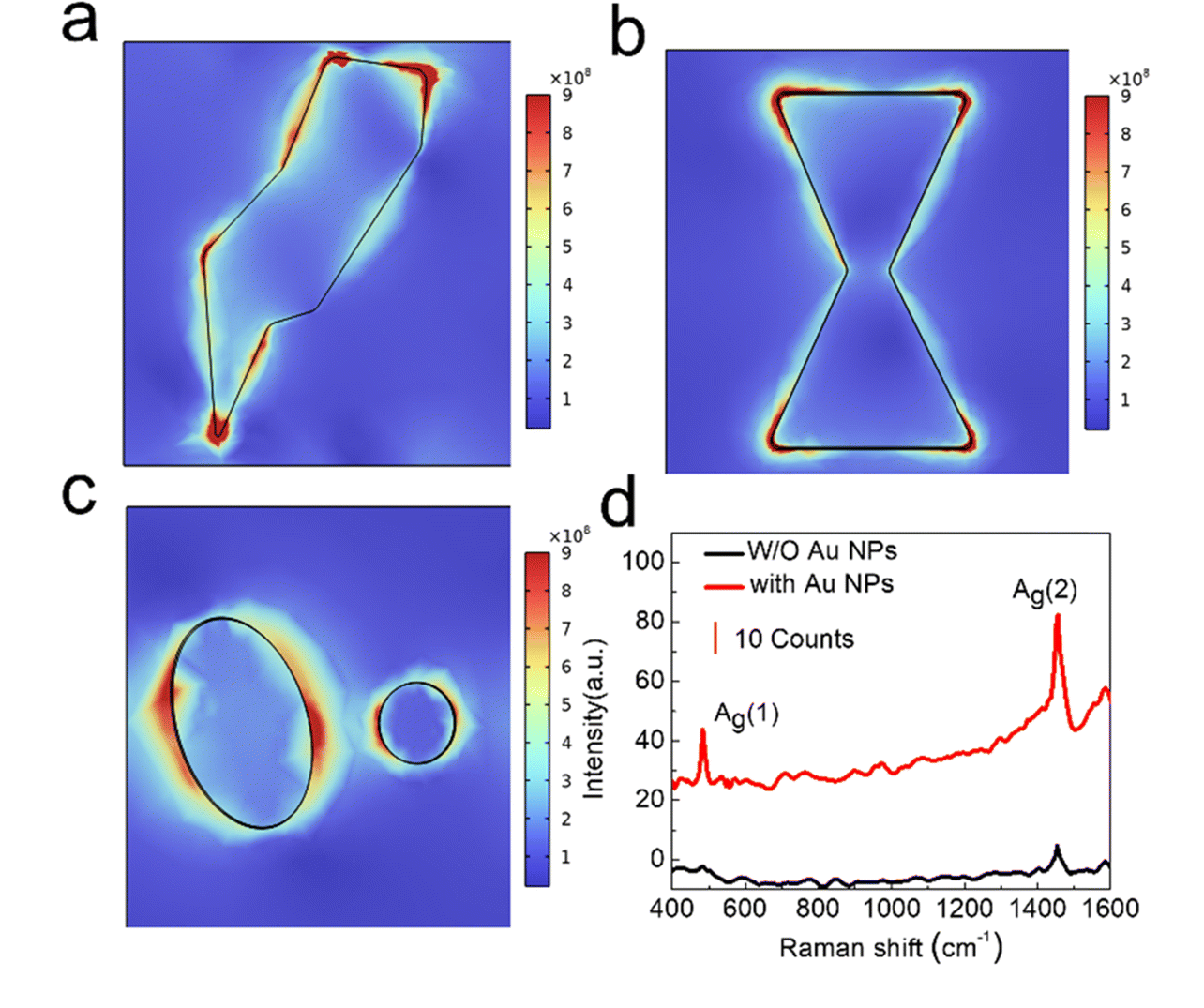 | ||
| Fig. 7 (a)–(c) Electrical field energy distribution at 532 nm of the Au NPs with different morphologies. (d) Raman spectrum acquired with a laser excitation of λ = 532 nm for the Ph-BTBT-12/C60 and Au NPs/Ph-BTBT-12/C60 films, respectively. | ||
C60 has attracted considerable attention due to its unique geometric shape and excellent physical and chemical properties.31 The SERS properties of C60 films are worth exploring. On the one hand, its spherical molecular structure makes it difficult to attach to the SERS substrate.32 On the other hand, it is insoluble in water and cannot obtain its SERS performance from water solution. Here, based on the prepared photodetector, we explored the SERS performance of C60 films with gold nanoparticles. The evaporation of the Ph-BTBT-12 film makes C60 more stable adsorption on it.
In the experiment, Raman measurements were performed on Ph-BTBT-12/C60 films with and without gold nanoparticles, and the excitation light source was a 532 nm wavelength laser. It can be seen from the Raman spectrum of Fig. 5d that both Raman spectra show two characteristic peaks of C60, namely Ag(1) (483.06 cm−1) and Ag(2) (1455.37 cm−1). The peak position of the Ag(1) has almost no change after adding gold nanoparticles. The peak position of the pentagonal pinch mode of the latter mode Ag(2) changes from 1452.65 cm−1 to 1455.37 cm−1. This is the characteristic frequency of the original C60 and this result matches with other literature reports. It is worth noting that the charge transfer factor cannot be ignored, and the peak position shift may be proof of adatom-charge-transfer.32 At the same time, it can also be seen that the Raman spectrum intensity of the sample with gold nanoparticles is significantly higher than that of the sample without gold nanoparticles. The Ag(1) peak is from almost no to an obvious peak, and the intensity of Ag(2) is increased from 4.8 to 82.3. The surface Raman enhancement effect is realized.
In order to explore the mechanism of Raman spectroscopy enhancement by gold nanoparticles, the finite element method software COMSOL was used for numerical simulations to explore the hot spot distribution of the electric field. Fig. 7 shows the electric field distribution xy cross-section of three typical gold nanoparticle morphologies at a wavelength of 532 nm. This is the excitation wavelength in the Raman spectrometer. It can be seen that the electric field enhancement of the polygonal gold nanoparticles appears at the vertex and each side length in Fig. 7a. Fig. 7b represents a dimer but it is not completely separated due to annealing time and temperature. In this case, the electric field enhancement appears above and below the gold nanoparticles. Fig. 7c shows the dimer formed with one large and one small irregular elliptical particle. The electric field hot spot distribution of this dimer in the 532 nm wavelength is different from that in the 365 nm wavelength. At this time, the electric field hot spot appears on both sides of the two gold nanoparticles, and the electric dipoles caused by the two nanoparticles interact with each other. At the same time, the electric field enhancement can also be seen at the gap between two nanoparticles, and its hot spot coverage is wider. These three cases all prove that the gold nanoparticles prepared by annealing produce hot spots in the 532 nm wavelength light field, and the electromagnetic field is greatly enhanced. The excitation of local surface plasmon resonance in various gold nanoparticle structures enhances the Raman signal intensity of the C60 film. It is worth noting that by changing the thickness of the gold film and the annealing temperature, a series of gold nanoparticles with regular size changes can be obtained as shown in Fig. S2 and S3 (ESI†). After continuous adjustment, the optimal gold nanoparticle size distribution can be found to achieve the best coupling with the excitation light, achieving higher light absorption and stronger Raman signal enhancement.
4 Conclusions
In summary, gold nanoparticles were integrated via one-step annealing into the Ph-BTBT-12/C60 vertical heterojunction photodetectors, marking the first application of the plasmonic effect of gold nanoparticles in organic ultraviolet photodetectors. This integration enables enhanced photoelectric detection and performance across the 265–520 nm waveband. At a wavelength of 365 nm, the device remains stable even after 60 days, with no deterioration in detection capability. It also successfully detects weak UV light with an intensity of 0.01 mW cm−2. The optical absorption at 365 nm increases by approximately 443.2% and the photoresponsivity improves by roughly 640 times, as shown by the current–time (I–t) curve, with a response time as short as 2 seconds. Additionally, the gold nanoparticles exhibit surface-enhanced Raman scattering (SERS) properties in C60 films. This work expands the application of gold nanoparticles in organic UV photodetectors and provides a valuable reference for the future development of flexible wearable devices, as well as imaging and health monitoring technologies. Although this strategy uses relatively expensive materials such as gold nanoparticles and C60, it exhibits very excellent photoelectric properties. In subsequent studies, new approaches to prepare and use lower-cost alternative accepter materials will help this strategy move toward a wider range of applications. In addition, new and effective materials to reduce costs and improve performance will be one of the important directions of future research.Author contributions
W. P. W. and F. H. L.: proposed, planned and supervised the project and designed the experiments. F. L., Y. W., C. L. Mao and F. L. Y.: carried out experiments, including fabrication of samples, carried out the measurement and collected the data. F. L. Y., F. H. L., and W. P. W.: analyzed the data and drafted the manuscript. All the authors participated in the data discussion and commented on the manuscript.Data availability
The authors confirm that the data supporting the findings of this study are available within the article and its ESI.†Conflicts of interest
There are no conflicts to declare.Acknowledgements
This work is supported by the National Natural Science Foundation of China (NSFC No. 52273242), the National Key R&D Program of China (No. 2021YFB2800703 and 2021YFB2800701) and the Chinese Academy of Sciences.References
- H. Chen, H. Liu, Z. Zhang, K. Hu and X. Fang, Adv. Mater., 2016, 28, 403–433 CrossRef CAS.
- X. Tang, J. Yang, Z. Duan, Y. Bu, Z. Yuan, Y. Jiang and H. Tai, Adv. Opt. Mater., 2024, 2401114 CrossRef CAS.
- D. Yang and D. Ma, Adv. Opt. Mater., 2019, 7, 1800522 CrossRef.
- Z. C. Chen, H. J. Liu, Y. C. Chang, B. J. Chen and S. J. Chang, ACS Appl. Nano Mater., 2023, 6, 9298–9305 CrossRef CAS.
- B. Deka Boruah, Nanoscale Adv., 2019, 1, 2059–2085 RSC.
- L. Jia, W. Zheng and F. Huang, PhotoniX, 2020, 1, 22 CrossRef.
- K. Baeg, M. Binda, D. Natali, M. Caironi and Y. Noh, Adv. Mater., 2013, 25, 4267–4295 CrossRef CAS PubMed.
- P. Han, Z. Zheng, Y. Lu, C. Lang, S. Gao, F. Guo, J. Wang and Y. Zhang, J. Mater. Chem. C, 2024, 12, 1543–1550 RSC.
- T. Liu, Q. Lin, Y. Ma, S. Wang, H. Chen, Y. Wei, Y. Song, L. Shen, F. Huang and H. Huang, Adv. Opt. Mater., 2022, 10, 2201104 CrossRef CAS.
- H. Wang, G. Rao, Y. Wang, X. Du, M. Zhang, X. Wang, A. Hu, Y. Hu, J. Huang, J. Chu, X. Wang, L. Qian and J. Xiong, J. Phys. Chem. C, 2021, 125, 4710–4719 CrossRef CAS.
- H. Y. Lan, Y. H. Hsieh, Z. Y. Chiao, D. Jariwala, M. H. Shih, T. J. Yen, O. Hess and Y. J. Lu, Nano Lett., 2021, 21, 3083–3091 CrossRef CAS PubMed.
- N. S. Azar, J. Bullock, S. Balendhran, H. Kim, A. Javey and K. B. Crozier, ACS Photonics, 2021, 8, 1120–1128 CrossRef CAS.
- M. R. Esopi and Q. Yu, ACS Appl. Nano Mater., 2019, 2, 4942–4953 CrossRef CAS.
- H. Wang, J. W. Lim, L. N. Quan, K. Chung, Y. J. Jang, Y. Ma and D. H. Kim, Adv. Opt. Mater., 2018, 6, 1701397 CrossRef.
- X. Luo, L. Du, Z. Wen, W. Lv, F. Zhao, X. Jiang, Y. Peng, L. Sun, Y. Li and J. Rao, Nanoscale, 2015, 7, 14422–14433 RSC.
- X. Luo, L. Du, Y. Liang, F. Zhao, W. Lv, K. Xu, Y. Wang and Y. Peng, ACS Appl. Mater. Interfaces, 2018, 10, 15352–15356 CrossRef CAS.
- J. K. Kim, K. S. Lee, T. H. Park, D. W. Jeong, Z. H. Kim and D. J. Jang, Opt. Laser Technol., 2019, 112, 151–158 CrossRef CAS.
- Y. Zhang, C. Wang, J. Wang, L. Chen, J. Li, Y. Liu, X. Zhao, Y. Wang and J. Yang, Spectrochim. Acta, Part A, 2016, 152, 461–467 CrossRef CAS PubMed.
- W. Wang and L. Qi, Adv. Funct. Mater., 2019, 29, 1807275 CrossRef.
- Z. Wang, Z. Dong, Y. Gu, Y. H. Chang, L. Zhang, L. J. Li, W. Zhao, G. Eda, W. Zhang, G. Grinblat, S. A. Maier, J. K. W. Yang, C. W. Qiu and A. T. S. Wee, Nat. Commun., 2016, 7, 11283 CrossRef CAS PubMed.
- S. M. Lewis, M. S. Hunt, G. A. DeRose, H. R. Alty, J. Li, A. Wertheim, L. De Rose, G. A. Timco, A. Scherer, S. G. Yeates and R. E. P. Winpenny, Nano Lett., 2019, 19, 6043–6048 CrossRef CAS PubMed.
- M. R. Esopi and Q. Yu, ACS Appl. Nano Mater., 2019, 2, 6690–6700 CrossRef CAS.
- J. Chen, W. Ouyang, W. Yang, J. H. He and X. Fang, Adv. Funct. Mater., 2020, 30, 1909909 CrossRef CAS.
- H. Zeng, H. Yu, B. Liu, S. Lu, X. Wei, L. Gao, M. Hong, X. Zhang, Z. Zhang and Y. Zhang, Adv. Funct. Mater., 2024, 34, 2400712 CrossRef CAS.
- L. Huang, F. Liu, J. Bao, X. Li and W. Wu, Materials, 2024, 17, 1395 CrossRef CAS PubMed.
- J. Low, J. Yu, M. Jaroniec, S. Wageh and A. A. Al-Ghamdi, Adv. Mater., 2017, 29, 1601694 CrossRef.
- L. Qian, W. Li, Z. Gu, J. Tian, X. Huang, P. T. Lai and W. Zhang, Adv. Opt. Mater., 2022, 10, 2102055 CrossRef CAS.
- C. Tian, D. Jiang, B. Li, J. Lin, Y. Zhao, W. Yuan, J. Zhao, Q. Liang, S. Gao, J. Hou and J. Qin, ACS Appl. Mater. Interfaces, 2014, 6, 2162–2166 CrossRef CAS PubMed.
- J. D. Hwang, M. J. Lai, H. Z. Chen and M. C. Kao, IEEE Photonics Technol. Lett., 2014, 26, 1023–1026 CAS.
- J. D. Hwang, F. H. Wang, C. Y. Kung and M. C. Chan, IEEE Trans. Nanotechnol., 2015, 14, 318–321 CAS.
- B. Li, J. Zhang, Z. Yan, M. Feng, Z. Yu and L. Wang, Crystals, 2020, 10, 182 CrossRef CAS.
- Z. Niu and Y. Fang, Vib. Spectrosc., 2007, 43, 415–419 CrossRef CAS.
Footnote |
| † Electronic supplementary information (ESI) available. See DOI: https://doi.org/10.1039/d4tc03972f |
| This journal is © The Royal Society of Chemistry 2025 |